TriQuint Semiconductor Texas: Phone (972)994-8465 Fax (972)994 8504 Web: www.triquint.com
Advance Product Information
Jan 17, 2005
1
Note: Devices designated as EPU are typically early in their characterization process prior to finalizing all electrical and process
specifications. Specifications are subject to change without notice.
27 - 31 GHz 1W Power Amplifier
TGA4509-EPU
Key Features
À
22 dB Nominal Gain @ 30 GHz
À
30 dBm Nominal Pout @ P1dB
À
25% PAE @ P1dB
À
-10 dB Nominal Return Loss
À
Built-in Power Detector
À
0.25-Ám mmW pHEMT 3MI
À
Bias Conditions: Vd = 4 - 6 V, Idq = 420 mA
À
Chip Dimensions 2.44 mm x 1.15 mm x 0.1 mm
(0.096 x 0.045 x 0.004 in)
Fixtured Measured Performance
Bias Conditions: Vd = 6 V, Id =420 mA
10
12
14
16
18
20
22
24
26
28
30
32
-12
-9
-6
-3
0
3
6
9
12
15
18
21
Pin (dBm )
Po
u
t
(
d
Bm)
& G
a
in
(
d
B)
0
200
400
600
800
1000
IDS (
m
A)
Gain
Pout
IDS
Data taken
@ 30 GHz
Primary Applications
À
Point to Point Radio
À
Point to Multi-point Radio
À
LMDS
À
Satellite Ground Terminal
-3 0
-2 5
-2 0
-1 5
-1 0
-5
0
5
1 0
1 5
2 0
2 5
3 0
2 5
2 6
2 7
2 8
2 9
3 0
3 1
3 2
3 3
3 4
F re q u e n c y (G H z )
Sij (
d
B)
S 2 1
S 1 1
S 2 2

TriQuint Semiconductor Texas: Phone (972)994-8465 Fax (972)994 8504 Web: www.triquint.com
Advance Product Information
Jan 17, 2005
2
Note: Devices designated as EPU are typically early in their characterization process prior to finalizing all electrical and process
specifications. Specifications are subject to change without notice.
TGA4509-EPU
TABLE II
ELECTRICAL CHARACTERISTICS
(T
A
= 25
o
C, Nominal)
TABLE I
MAXIMUM RATINGS 1/
Symbol
Parameter
Value
Notes
V
+
Positive Supply Voltage
7 V
V
-
Negative Supply Voltage Range
-5 V to 0 V
|Ig|
Gate Current
35.2 mA
I
+
Positive Supply Current
930 mA
2/, 5/
P
D
Power Dissipation
TBD
P
IN
Input Continuous Wave Power
22 dBm
T
CH
Operating Channel Temperature
150
░
C
3/, 4/
T
M
Mounting Temperature (30 seconds)
320
░
C
T
STG
Storage Temperature
-65
░
C to 150
░
C
1/
These values represent the maximum operable values of this device
2/
Total current for the entire MMIC
3/
These ratings apply to each individual FET
4/
Junction operating temperature will directly affect the device mean time to
failure (MTTF). For maximum life it is recommended that junction
temperatures be maintained at the lowest possible levels.
5/
The maximum supply current from one side is 650 mA. From both sides, the
maximum supply current is 930 mA.
Parameter
Units
Typical
Drain Operating Voltage
V
6
Quiescent Current
mA
420
Small Signal Gain @ 30 GHz
dB
22
Gain Flatness
dB/50MHz
0.0660
Input Return Loss (Linear Small Signal)
dB
-10
Output Return Loss (Linear Small Signal)
dB
-10
Reverse Isolation
dB
-40
CW Output Power @ P1dB
dBm
30
Power Added Efficiency @ P1dB
%
25
P1dB temperature coeff. TC (-40 to +85 ░C)
dB/deg C
0.0135

TriQuint Semiconductor Texas: Phone (972)994-8465 Fax (972)994 8504 Web: www.triquint.com
Advance Product Information
Jan 17, 2005
3
Note: Devices designated as EPU are typically early in their characterization process prior to finalizing all electrical and process
specifications. Specifications are subject to change without notice.
Measured Fixtured Data
Bias Conditions: Vd = 6 V, Id = 420 mA
TGA4509-EPU
6
8
10
12
14
16
18
20
22
24
26
26
27
28
29
30
31
32
33
34
Frequency (GHz)
G
a
in
(d
B)
-30
-25
-20
-15
-10
-5
0
25
26
27
28
29
30
31
32
33
34
Frequency (GHz)
Return Loss (dB)
S11
S22

TriQuint Semiconductor Texas: Phone (972)994-8465 Fax (972)994 8504 Web: www.triquint.com
Advance Product Information
Jan 17, 2005
4
Note: Devices designated as EPU are typically early in their characterization process prior to finalizing all electrical and process
specifications. Specifications are subject to change without notice.
TGA4509-EPU
Measured Fixtured Data
Bias Conditions: Vd = 6 V, Id = 420 mA
26
27
28
29
30
31
32
27 27.5 28 28.5 29 29.5 30 30.5 31 31.5 32 32.5 33 33.5
Frequency (GHz)
Power (dBm)
Pout @ P1dB (dBm)
Psat
TriQuint Semiconductor Texas: Phone (972)994-8465 Fax (972)994 8504 Web: www.triquint.com
Advance Product Information
Jan 17, 2005
5
Note: Devices designated as EPU are typically early in their characterization process prior to finalizing all electrical and process
specifications. Specifications are subject to change without notice.
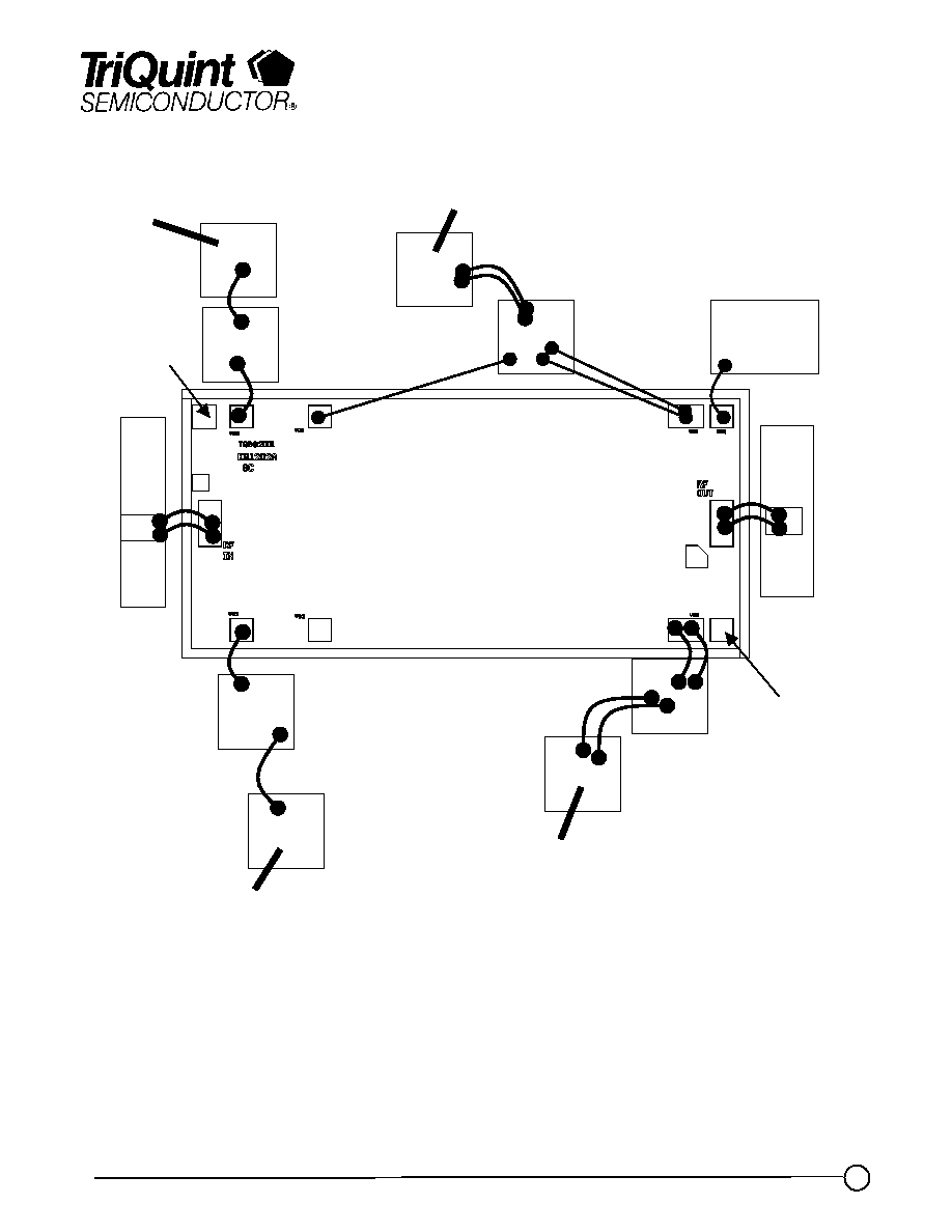
Notes:
1. Connection to power det, ref diode shown.
2. 1
Á
F cap on gate & drain power supplies are lines required.
3. Gate voltage can either be from one side or both sides.
4. Drain voltage is required from both sides for Id > 650 mA.
Output
TFN
100pF
100pF
Vg
100pF
Vd
Vd (optional)
100pF
Vg (optional)
0.01
P
F DQ
cap
(opt.)
GaAs MMIC devices are susceptible to damage from Electrostatic Discharge. Proper precautions should
be observed during handling, assembly and test.
Recommended Assembly Diagram
Input
TFN
0.01
P
F
0.01
P
F
0.01
P
F
0.01
P
F
TGA4509-EPU
Power
Detector
Reference
Diode