TriQuint Semiconductor Texas: Phone (972)994-8465 Fax (972)994 8504 Email: Info-mmw@tqs.com Web: www.triquint.com
Advance Product Information
January 7, 2004
1
Note: Devices designated as EPU are typically early in their characterization process prior to finalizing all electrical and process
specifications. Specifications are subject to change without notice
1.0
1.5
2.0
2.5
3.0
26
28
30
32
34
36
38
40
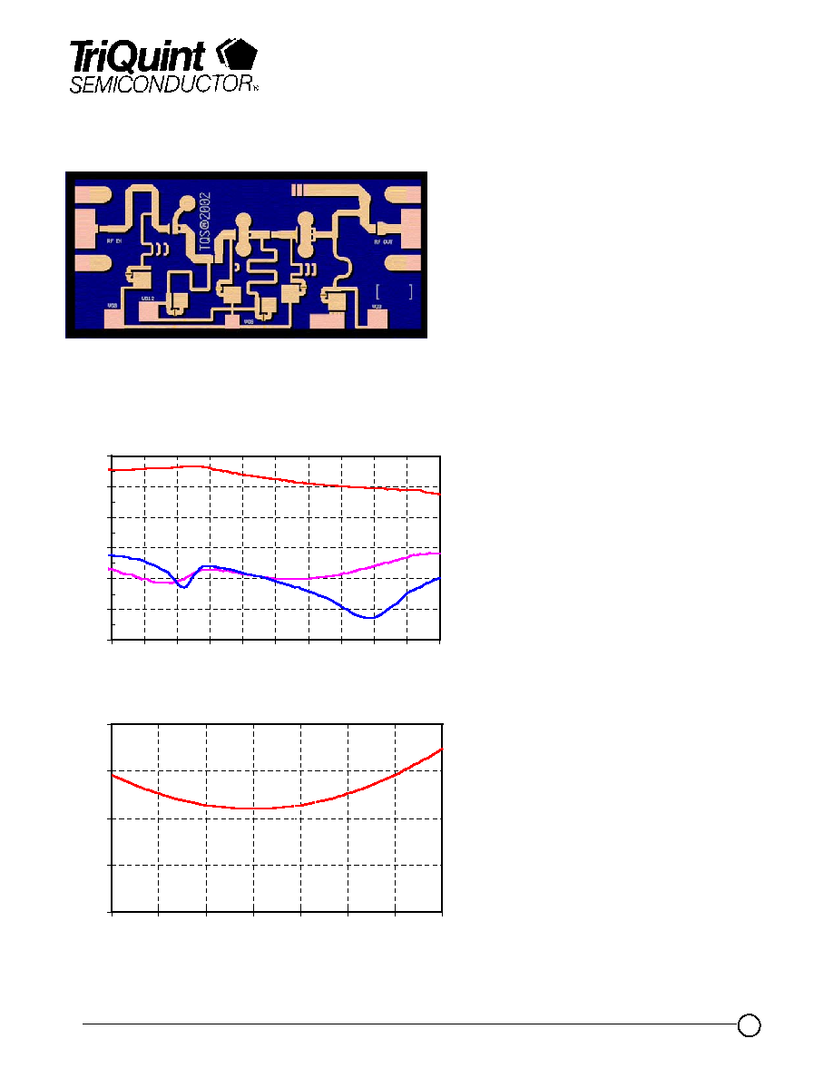
Frequency (GHz)
N
o
i
s
e
Fi
gu
r
e
(
d
B
)
-30
-20
-10
0
10
20
30
20
22
24
26
28
30
32
34
36
38
40
Frequency (GHz)
G
a
in &
R
e
t
u
r
n
Lo
s
s
(
d
B
)
Ka Band Low Noise Amplifier TGA4507-EPU
Key Features
�
Typical Frequency Range: 28 - 36 GHz
�
2.3 dB Nominal Noise Figure
�
22 dB Nominal Gain
�
12 dBm Nominal P1dB
�
Bias 3.0 V, 60 mA
�
0.15 um 3MI pHEMT Technology
�
Chip Dimensions 1.86 x 0.85 x 0.1 mm
(0.073 x 0.033 x 0.004 in)
Primary Applications
�
Point-to-Point Radio
�
Point-to-MultiPoint Radio
�
Ka Band VSAT
Preliminary Measured Data
Bias Conditions: Vd = 3.0 V, Id = 60 mA
ORL
Gain
IRL
TriQuint Semiconductor Texas: Phone (972)994-8465 Fax (972)994 8504 Email: Info-mmw@tqs.com Web: www.triquint.com
Advance Product Information
January 7, 2004
2
Note: Devices designated as EPU are typically early in their characterization process prior to finalizing all electrical and process
specifications. Specifications are subject to change without notice
TABLE I
MAXIMUM RATINGS 1/
SYMBOL
PARAMETER
VALUE
NOTES
Vd
Drain Voltage
5 V
2/
Vg
Gate Voltage Range
-1 TO +0.5 V
Id
Drain Current
280 mA
2/ 3/
�Ig�
Gate Current
6 mA
3/
P
IN
Input Continuous Wave Power
TBD
P
D
Power Dissipation
TBD
2/ 4/
T
CH
Operating Channel Temperature
150
0
C
5/ 6/
T
M
Mounting Temperature (30 Seconds)
320
0
C
T
STG
Storage Temperature
-65 to 150
0
C
1/
These ratings represent the maximum operable values for this device.
2/
Combinations of supply voltage, supply current, input power, and output power shall not exceed P
D
.
3/
Total current for the entire MMIC.
4/
When operated at this bias condition with a base plate temperature of TBD, the median life is
reduced from TBD to TBD hrs.
5/
Junction operating temperature will directly affect the device median time to failure (MTTF). For
maximum life, it is recommended that junction temperatures be maintained at the lowest possible
levels.
6/
These ratings apply to each individual FET.
TGA4507-EPU

TriQuint Semiconductor Texas: Phone (972)994-8465 Fax (972)994 8504 Email: Info-mmw@tqs.com Web: www.triquint.com
Advance Product Information
January 7, 2004
3
Note: Devices designated as EPU are typically early in their characterization process prior to finalizing all electrical and process
specifications. Specifications are subject to change without notice
TABLE III
ELECTRICAL CHARACTERISTICS
(Ta = 25
0
C Nominal)
TGA4507-EPU
PARAMETER
TYPICAL
UNITS
Drain Voltage, Vd
3.0
V
Drain Current, Id
60
mA
Gate Voltage, Vg
-0.5 to 0
V
Small Signal Gain, S21
22
dB
Input Return Loss, S11
8
dB
Output Return Loss, S22
8
dB
Noise Figure, NF
2.3
dB
Output Power @ 1 dB Compression Gain, P1dB
12
dBm
Q1 is 100 um FET, Q2 is 200 um FET, Q3 is 300 um FET.
TABLE II
DC PROBE TESTS
(Ta = 25
0
C, Nominal)
SYMBOL
PARAMETER
MIN.
TYP.
MAX.
UNITS
V
BVGD3
Breakdown Voltage Gate-Source
-5
V
V
P1,2,3
Pinch-off Voltage
-0.4
V
TriQuint Semiconductor Texas: Phone (972)994-8465 Fax (972)994 8504 Email: Info-mmw@tqs.com Web: www.triquint.com
Advance Product Information
January 7, 2004
4
Note: Devices designated as EPU are typically early in their characterization process prior to finalizing all electrical and process
specifications. Specifications are subject to change without notice
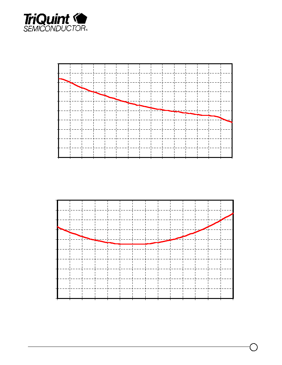
TGA4507-EPU
Preliminary Measured Data
Bias Conditions: Vd = 3.0 V, Id = 60 mA
10
12
14
16
18
20
22
24
26
28
30
25 26 27 28 29 30 31 32 33 34 35 36 37 38 39 40
Fre quency (GHz)
G
a
in
(
d
B
)
1.0
1.2
1.4
1.6
1.8
2.0
2.2
2.4
2.6
2.8
3.0
26 27 28
29 30 31 32
33 34 35 36 37 38 39 40
Fre que ncy (GHz)
N
o
i
se F
i
g
u
r
e
(
d
B)

TriQuint Semiconductor Texas: Phone (972)994-8465 Fax (972)994 8504 Email: Info-mmw@tqs.com Web: www.triquint.com
Advance Product Information
January 7, 2004
5
Note: Devices designated as EPU are typically early in their characterization process prior to finalizing all electrical and process
specifications. Specifications are subject to change without notice
TGA4507-EPU
Preliminary Measured Data
Bias Conditions: Vd = 3.0 V, Id = 60 mA
-30
-25
-20
-15
-10
-5
0
25 26 27 28 29 30 31 32 33 34 35 36 37 38 39 40
Fre quency (GHz)
I
n
p
u
t Re
tu
r
n
L
o
s
s
(
d
B)
-30
-25
-20
-15
-10
-5
0
25 26 27 28 29 30 31 32 33 34 35 36 37 38 39 40
Fre quency (GHz)
O
u
tp
u
t
Re
tu
r
n
L
o
s
s
(d
B)