TriQuint Semiconductor Texas: Phone (972)994-8465 Fax (972)994-8504 Email: Info-mmw@tqs.com Web: www.triquint.com
Advance Product Information
September 1, 2005
1
30
31
32
33
34
35
36
37
38
39
40
9
9.2
9.4
9.6
9.8
10
10.2
10.4
10.6
Frequency (GHz )
C
W
S
a
tu
r
a
te
d
O
u
tp
u
t
P
o
w
e
r
(d
B
m
)
7V, 1.4A
8V, 1.4A
9V, 1.05A
-30
-25
-20
-15
-10
-5
0
5
10
15
20
25
30
9
9.2
9.4
9.6
9.8
10
10.2
10.4 10.6
Frequency (GHz )
C
W
S-
Pa
r
a
m
e
t
e
r
s
(
d
B
)
S21
S11
S22
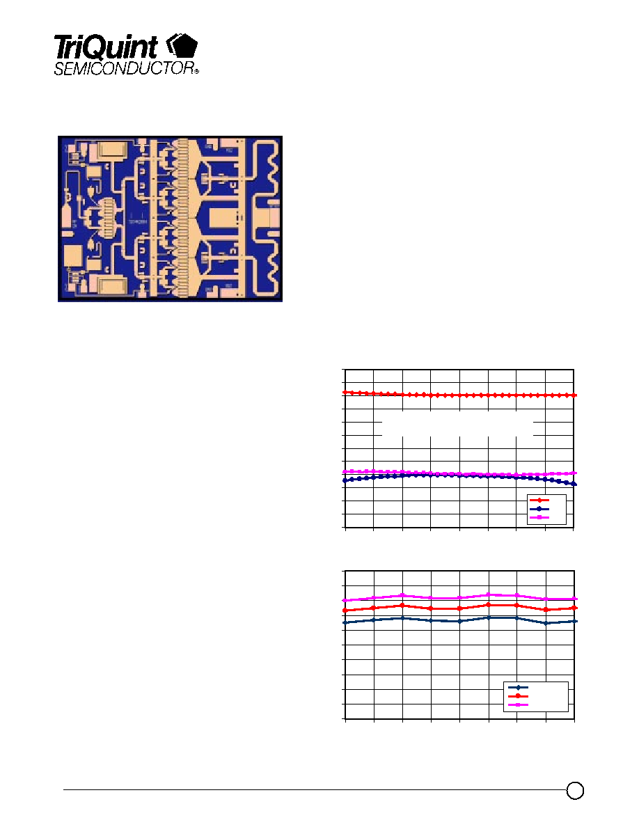
9 ¡ 10.5GHz High Power Amplifier TGA2704
Key Features
À
Frequency Range: 9.0 -10.5 GHz
À
38 dBm Nominal Output Power
À
20 dB Nominal Gain
À
Bias: 7-9V, 1.4A & 1.05A
(~ 2A under RF drive)
À
0.25 um 3MI pHEMT Technology
À
Chip Dimensions 3.52 x 2.61 x 0.10 mm
(0.139 x 0.103 x 0.004 in)
Primary Applications
À
Point-to-Point Radio
À
Communications
Measured Fixtured Data
Note: Devices is early in the characterization process prior to finalizing all electrical specifications. Specifications are subject to change
without notice
Product Description
The TriQuint TGA2704 is a High Power
Amplifier MMIC for 9 ¡ 10.5GHz applications.
The part is designed using TriQuint's 0.25um
3MI pHEMT production process.
The TGA2704 nominally provides 38 dBm
output power and 40% PAE for bias of 9V,
1.05A. The typical gain is 20 dB.
The part is ideally suited for low cost markets
such as Point-to-Point Radio and
Communications.
The TGA2704 is 100% DC and RF tested on-
wafer to ensure performance compliance.
The TGA2704 has a protective surface
passivation layer providing environmental
robustness.
Lead-Free & RoHS compliant.
Vd = 7 V, Id = 1.4A
TriQuint Semiconductor Texas: Phone (972)994-8465 Fax (972)994-8504 Email: Info-mmw@tqs.com Web: www.triquint.com
Advance Product Information
September 1, 2005
2
TABLE I
MAXIMUM RATINGS 1/
SYMBOL
PARAMETER
VALUE
NOTES
Vd
Drain Voltage
10 V
2/
Vg
Gate Voltage Range
-1 TO +0.5 V
Id
Drain Current
3.85 A
2/ 3/
Ig
Gate Current
85 mA
3/
P
IN
Input Continuous Wave Power
23 dBm
P
D
Power Dissipation
11.3 W
2/ 4/
T
CH
Operating Channel Temperature
150
0
C
5/
T
M
Mounting Temperature (30 Seconds)
320
0
C
T
STG
Storage Temperature
-65 to 150
0
C
1/
These ratings represent the maximum operable values for this device.
2/
Combinations of supply voltage, supply current, input power, and output power shall not exceed P
D
.
3/
Total current for the entire MMIC.
4/
When operated at this power dissipation with a base plate temperature of 60
0
C, the median life is
1.0E+6 hrs.
5/
Junction operating temperature will directly affect the device median time to failure (MTTF). For
maximum life, it is recommended that junction temperatures be maintained at the lowest possible
levels.
TGA2704
TriQuint Semiconductor Texas: Phone (972)994-8465 Fax (972)994-8504 Email: Info-mmw@tqs.com Web: www.triquint.com
Advance Product Information
September 1, 2005
3
TABLE II
ELECTRICAL CHARACTERISTICS
(Ta = 25
0
C Nominal)
TGA2704
TABLE III
THERMAL INFORMATION
PARAMETER
TEST CONDITIONS
T
CH
(
O
C)
T
JC
(
q
C/W)
T
M
(HRS)
JC
Thermal Resistance
(channel to Case)
Vd = 7 V
Id = 1.4 A
P
diss
= 9.8W
Small Signal
140
7.1
2.4E+6
JC
Thermal Resistance
(channel to Case)
Vd = 7 V
Id = 1.7 A @ Psat
P
diss
= 7.2 W
P
out
= 4.8 W (RF)
121
7.1
1.4E+7
Note: Assumes eutectic attach using 1.5 mil 80/20 AuSn mounted to a 20 mil CuMo
Carrier at 70
o
C baseplate temperature.
.
PARAMETER
TYPICAL
TYPICAL
UNITS
Frequency Range
9.0 ¡ 10.5
9.0 ¡ 10.5
GHz
Drain Voltage, Vd
7
9
V
Drain Current, Id
1.4
1.05
A
Gate Voltage, Vg
-0.6
-0.6
V
Small Signal Gain, S21
20
19
dB
Input Return Loss, S11
10
10
dB
Output Return Loss, S22
10
10
dB
CW Saturated Output Power @ 19 dBm Pin
36.5
38
dBm
Pulsed Saturated Output Power @ 19 dBm Pin
& 25% Duty Cycle
36.7
38.5
dBm
CW Power Added Eff. @ 19 dBm Pin
40
39
%
Pulsed Power Added Eff. @ 19 dBm Pin & 25%
Duty Cycle
39
38
%
Small Signal Gain Temperature Coefficient
-0.03
-0.03
dB/
0
C
TriQuint Semiconductor Texas: Phone (972)994-8465 Fax (972)994-8504 Email: Info-mmw@tqs.com Web: www.triquint.com
Advance Product Information
September 1, 2005
4
-30
-28
-26
-24
-22
-20
-18
-16
-14
-12
-10
-8
-6
-4
-2
0
9
9.2
9.4
9.6
9.8
10
10.2
10.4
10.6
Frequency (GHz)
C
W
R
e
tur
n
L
o
s
s
(dB
)
0
2
4
6
8
10
12
14
16
18
20
22
24
26
28
30
9
9.2
9.4
9.6
9.8
10
10.2
10.4
10.6
Frequency (GHz)
C
W
Gain
(
d
B
)
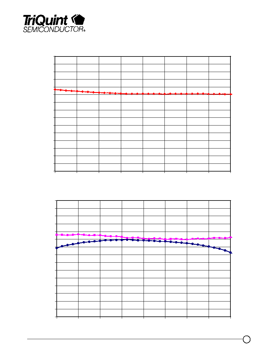
TGA2704
Measured Data
Bias Conditions: Vd = 7V, Idq = 1.4 A
S11
S22
TriQuint Semiconductor Texas: Phone (972)994-8465 Fax (972)994-8504 Email: Info-mmw@tqs.com Web: www.triquint.com
Advance Product Information
September 1, 2005
5
30
31
32
33
34
35
36
37
38
39
40
9
9.2
9.4
9.6
9.8
10
10.2
10.4
10.6
Frequency (GHz)
C
W
S
a
tu
ra
te
d
O
u
tp
u
t
P
o
w
e
r (
d
B
m
)
7V, 1.4A
8V, 1.4A
9V, 1.05A
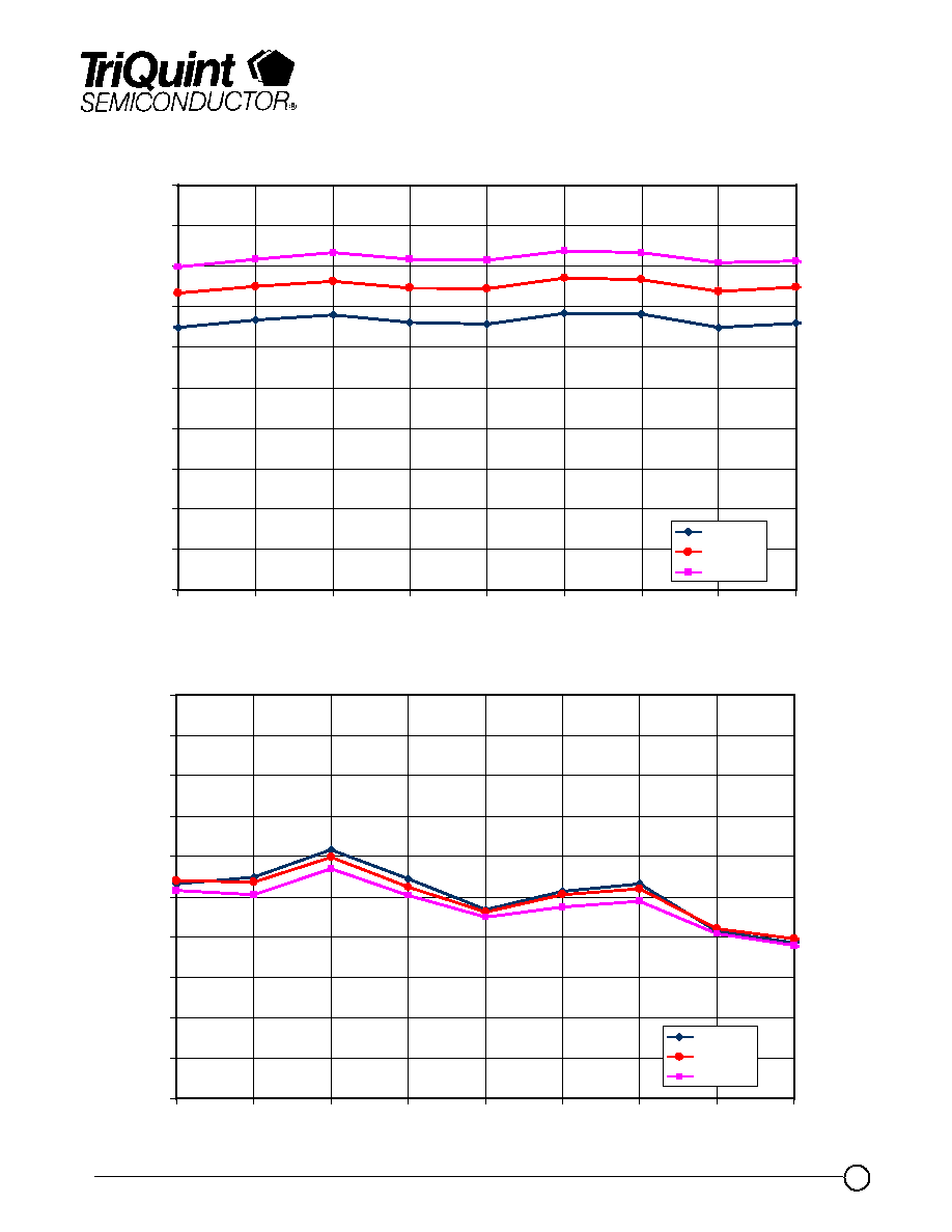
TGA2704
Measured Data
Pin = 19dBm, CW Power
30
32
34
36
38
40
42
44
46
48
50
9
9.2
9.4
9.6
9.8
10
10.2
10.4
10.6
Frequency (GHz)
C
W
P
o
w
e
r A
d
d
e
d
E
ff.
(%
)
7V, 1.4A
8V, 1.4A
9V, 1.05A
TriQuint Semiconductor Texas: Phone (972)994-8465 Fax (972)994-8504 Email: Info-mmw@tqs.com Web: www.triquint.com
Advance Product Information
September 1, 2005
6
12
14
16
18
20
22
24
26
28
30
32
34
36
38
40
0
2
4
6
8
10
12
14
16
18
20
Pin (dBm)
CW
Pou
t
(dB
m
)
&
G
a
i
n
(dB)
1.00
1.10
1.20
1.30
1.40
1.50
1.60
1.70
1.80
1.90
2.00
2.10
2.20
2.30
2.40
Id
(A)
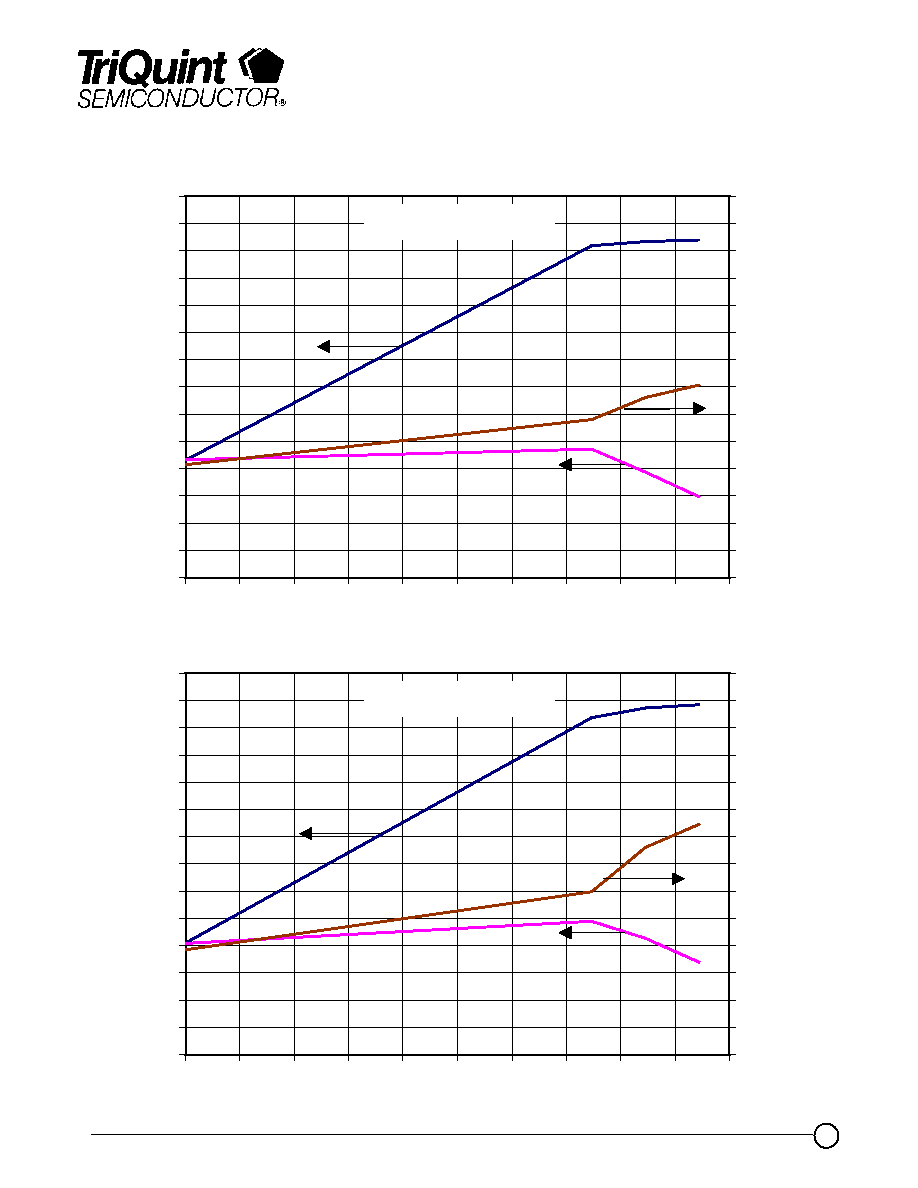
TGA2704
Measured Data
Frequency @ 10GHz, CW Power
Vd = 7V, Id = 1.4A
12
14
16
18
20
22
24
26
28
30
32
34
36
38
40
0
2
4
6
8
10
12
14
16
18
20
Pin (dBm)
CW
Pou
t
(dB
m
)
&
G
a
i
n
(dB)
1.00
1.10
1.20
1.30
1.40
1.50
1.60
1.70
1.80
1.90
2.00
2.10
2.20
2.30
2.40
Id
(A)
Vd = 8V, Id = 1.4A
Pout
Gain
Id
Pout
Id
Gain
TriQuint Semiconductor Texas: Phone (972)994-8465 Fax (972)994-8504 Email: Info-mmw@tqs.com Web: www.triquint.com
Advance Product Information
September 1, 2005
7
12
14
16
18
20
22
24
26
28
30
32
34
36
38
40
0
2
4
6
8
10
12
14
16
18
20
Pin (dBm)
CW
P
o
ut
(
d
Bm
) &
G
a
i
n
(d
B)
1.00
1.10
1.20
1.30
1.40
1.50
1.60
1.70
1.80
1.90
2.00
2.10
2.20
2.30
2.40
Id
(
A
)
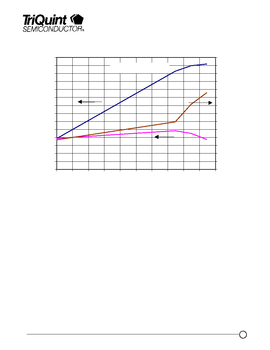
TGA2704
Measured Data
Frequency @ 10GHz, CW Power
Pout
Id
Gain
Vd = 9V, Id = 1.05A
TriQuint Semiconductor Texas: Phone (972)994-8465 Fax (972)994-8504 Email: Info-mmw@tqs.com Web: www.triquint.com
Advance Product Information
September 1, 2005
8
30
31
32
33
34
35
36
37
38
39
40
9
9.2
9.4
9.6
9.8
10
10.2
10.4
10.6
Frequency (GHz)
P
u
l
s
ed S
a
tur
ate
d
O
u
tp
ut P
o
w
e
r
(d
B
m
)
7V, 1.4A
8V, 1.4A
9V, 1.05A
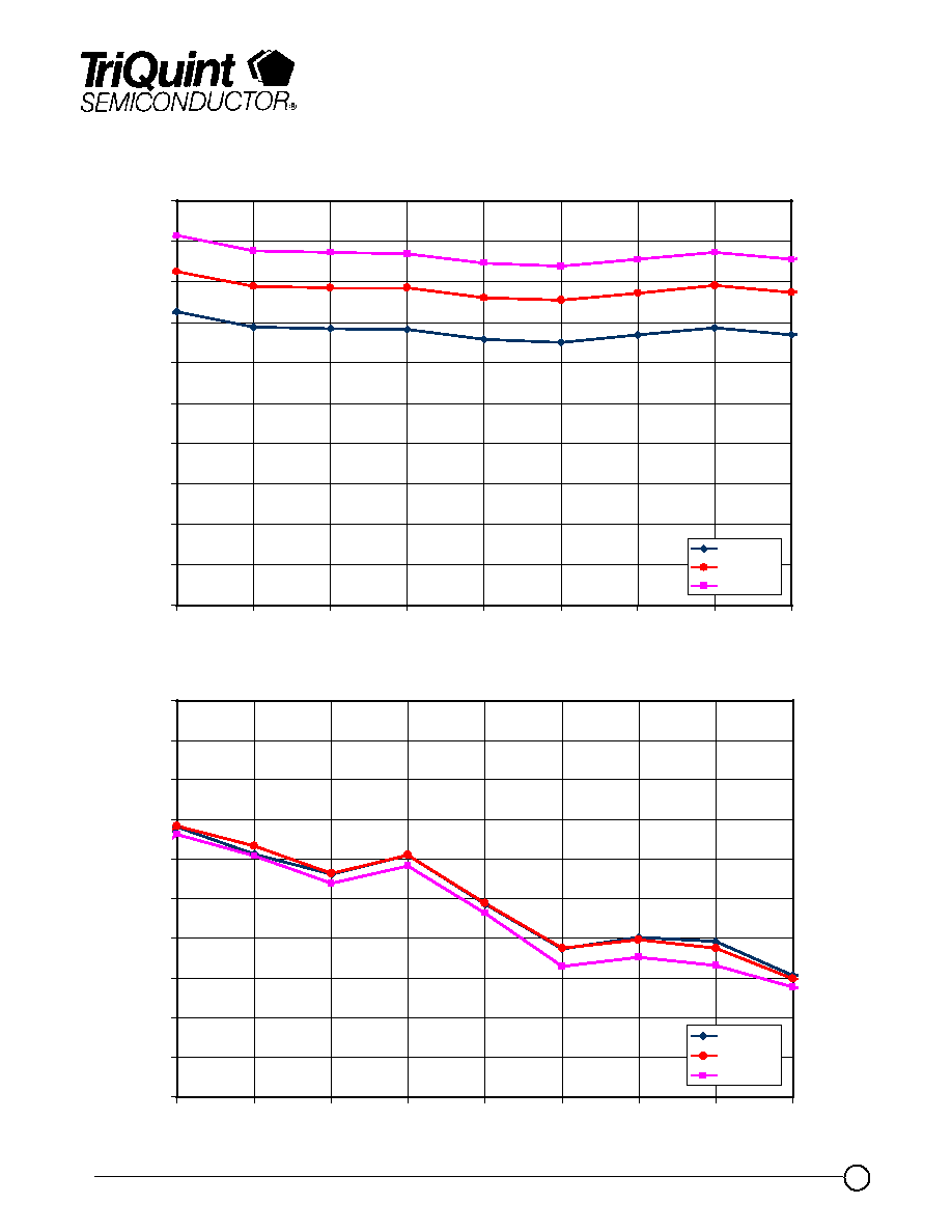
TGA2704
Measured Data
Pin = 19dBm, Pulsed Power, 25% DC
30
32
34
36
38
40
42
44
46
48
50
9
9.2
9.4
9.6
9.8
10
10.2
10.4
10.6
Frequency (GHz)
P
u
l
s
e
d
Po
w
e
r
Ad
de
d Ef
f
.
(
%
)
7V, 1.4A
8V, 1.4A
9V, 1.05A

TriQuint Semiconductor Texas: Phone (972)994-8465 Fax (972)994-8504 Email: Info-mmw@tqs.com Web: www.triquint.com
Advance Product Information
September 1, 2005
9
12
14
16
18
20
22
24
26
28
30
32
34
36
38
40
0
2
4
6
8
10
12
14
16
18
20
Pin (dBm)
P
u
ls
e
d
P
o
ut
(dB
m
)
&
G
a
in (dB
)
1.00
1.10
1.20
1.30
1.40
1.50
1.60
1.70
1.80
1.90
2.00
2.10
2.20
2.30
2.40
Id (
A
)
12
14
16
18
20
22
24
26
28
30
32
34
36
38
40
0
2
4
6
8
10
12
14
16
18
20
Pin (dBm)
Pu
l
s
e
d
Pou
t
(d
B
m
)
&
G
a
i
n
(
d
B)
1.00
1.10
1.20
1.30
1.40
1.50
1.60
1.70
1.80
1.90
2.00
2.10
2.20
2.30
2.40
Id (A
)
TGA2704
Measured Data
Frequency @ 10GHz, Pulsed Power, 25% DC
Pout
Gain
Id
Pout
Id
Gain
Vd = 7V, Id = 1.4A
Vd = 8V, Id = 1.4A
TriQuint Semiconductor Texas: Phone (972)994-8465 Fax (972)994-8504 Email: Info-mmw@tqs.com Web: www.triquint.com
Advance Product Information
September 1, 2005
10
12
14
16
18
20
22
24
26
28
30
32
34
36
38
40
0
2
4
6
8
10
12
14
16
18
20
Pin (dBm)
P
u
ls
ed
P
o
u
t
(
d
B
m
)
&
G
a
in
(
d
B
)
1.00
1.10
1.20
1.30
1.40
1.50
1.60
1.70
1.80
1.90
2.00
2.10
2.20
2.30
2.40
Id (A
)
TGA2704
Measured Data
Frequency @ 10GHz, Pulsed Power, 25% DC
Vd = 9V, Id = 1.05A
Pout
Gain
Id
TriQuint Semiconductor Texas: Phone (972)994-8465 Fax (972)994-8504 Email: Info-mmw@tqs.com Web: www.triquint.com
Advance Product Information
September 1, 2005
11
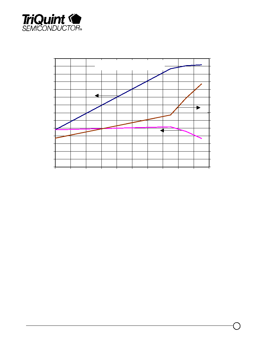
35
36
37
38
39
40
41
42
43
44
45
15
16
17
18
19
20
21
22
23
24
25
26
27
28
Output Power/Tone (dBm)
T
O
I
@
1
0
G
Hz
(
d
Bm
)
7V, 1.4A
8V, 1.4A
9V, 1.05A
TGA2704
Measured Data
Frequency @ 10GHz, CW TOI
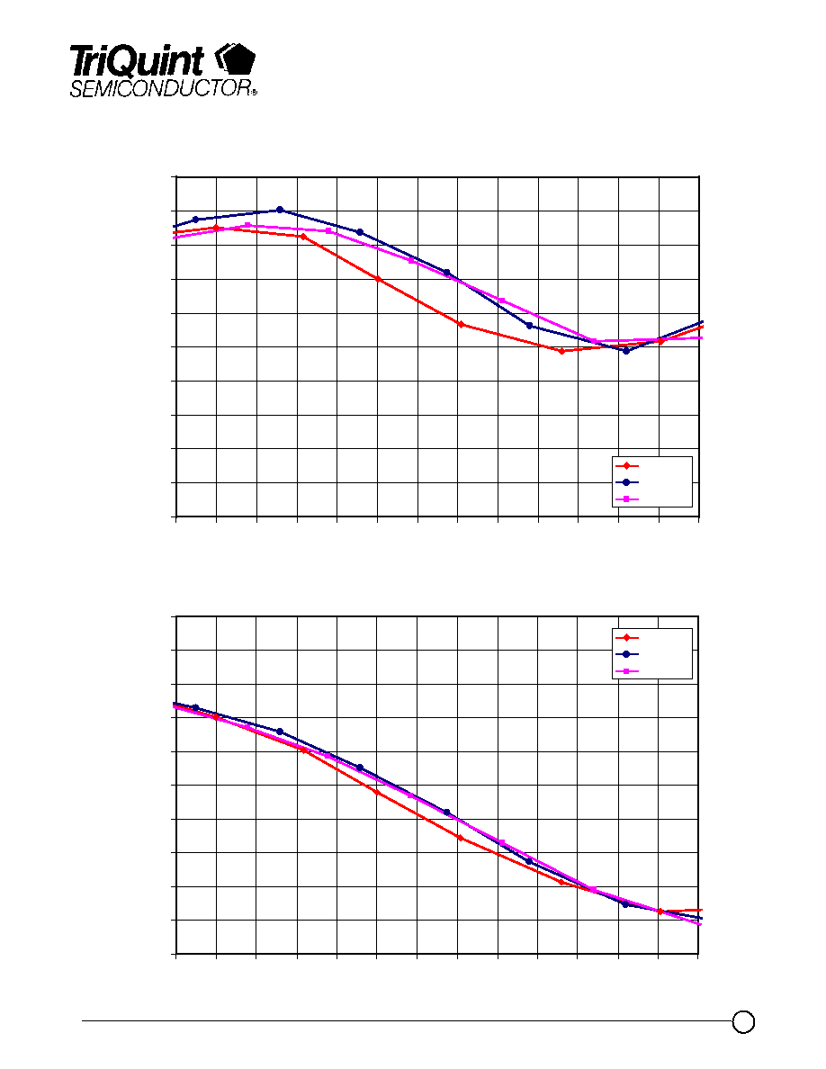
20
25
30
35
40
45
50
55
60
65
70
15
16
17
18
19
20
21
22
23
24
25
26
27
28
Output Power/Tone (dBm)
CW
I
M
R3
@
1
0
G
Hz
(
d
Bc
)
7V, 1.4A
8V, 1.4A
9V, 1.05A
TriQuint Semiconductor Texas: Phone (972)994-8465 Fax (972)994-8504 Email: Info-mmw@tqs.com Web: www.triquint.com
Advance Product Information
September 1, 2005
12
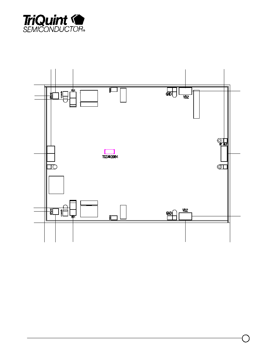
Mechanical Drawing
TGA2704
GaAs MMIC devices are susceptible to damage from Electrostatic Discharge. Proper precautions should
be observed during handling, assembly and test.
0.213
(0.008)
0.544
(0.021)
2.677
(0.105)
3.524
(0.139)
0.119
(0.005)
1.305
(0.051)
2.491
(0.098)
3.411
(0.134)
0.125
(0.005)
2.610
(0.103)
2.401
(0.095)
0.209
(0.008)
0
0
(0.051)
1.305
Units: Millimeters (inches)
Thickness: 0.10 (0.004)
Chip edge to bond pad dimensions are shown to center of bond pad
Chip size tolerance: +/- 0.05 (0.002)
GND IS BACKSIDE OF MMIC
Bond pad # 1
Bond pad # 2, 8
Bond pad # 3, 7
Bond pad # 4, 6
Bond pad # 5
(RF Input)
(Vg)
(Vd1)
(Vd2)
(RF Output)
0.150 x 0.300 (0.006 x 0.012)
0.120 x 0.120 (0.005 x 0.005)
0.120 x 0.290 (0.005 x 0.011)
0.250 x 0.140 (0.010 x 0.006)
0.125 x 0.300 (0.005 x 0.012)
R
F P
(0.008)
0.213
(0.021)
0.544
(0.105)
2.677
1
2
3
4
5
6
7
8
0.278
(0.011)
2.332
(0.092)
TriQuint Semiconductor Texas: Phone (972)994-8465 Fax (972)994-8504 Email: Info-mmw@tqs.com Web: www.triquint.com
Advance Product Information
September 1, 2005
13
Recommended Chip Assembly Diagram
TGA2704
GaAs MMIC devices are susceptible to damage from Electrostatic Discharge. Proper precautions should
be observed during handling, assembly and test.
Vd = 7 to 9 V
Vg = -0.6 V Typical
1000pF
1000pF
1000pF
1000pF
1000pF
1000pF
Vg
RF In
Vg
Vd
RF Out
Vd

TriQuint Semiconductor Texas: Phone (972)994-8465 Fax (972)994-8504 Email: Info-mmw@tqs.com Web: www.triquint.com
Advance Product Information
September 1, 2005
14
Assembly Process Notes
GaAs MMIC devices are susceptible to damage from Electrostatic Discharge. Proper precautions should
be observed during handling, assembly and test.
TGA2704
Reflow process assembly notes:
À
Use AuSn (80/20) solder with limited exposure to temperatures at or above 300
0
C (30 seconds max).
À
An alloy station or conveyor furnace with reducing atmosphere should be used.
À
No fluxes should be utilized.
À
Coefficient of thermal expansion matching is critical for long-term reliability.
À
Devices must be stored in a dry nitrogen atmosphere.
Component placement and adhesive attachment assembly notes:
À
Vacuum pencils and/or vacuum collets are the preferred method of pick up.
À
Air bridges must be avoided during placement.
À
The force impact is critical during auto placement.
À
Organic attachment can be used in low-power applications.
À
Curing should be done in a convection oven; proper exhaust is a safety concern.
À
Microwave or radiant curing should not be used because of differential heating.
À
Coefficient of thermal expansion matching is critical.
Interconnect process assembly notes:
À
Thermosonic ball bonding is the preferred interconnect technique.
À
Force, time, and ultrasonics are critical parameters.
À
Aluminum wire should not be used.
À
Maximum stage temperature is 200
0
C.