Advance Product Information
January 19, 2006
1
TriQuint Semiconductor Texas: Phone (972)994-8465 Fax (972)994-8504 Email: Info-mmw@tqs.com Web: www.triquint.com
2-20 GHz LNA with AGC
TGA2513-SM
Key Features
·
Frequency Range: 2-20 GHz
·
17 dB Nominal Gain
·
> 30 dB Adjustable Gain with Vg2
·
16 dBm Nominal P1dB
·
2.5 dB Midband Noise Figure
·
Bias Conditions: Vd=5V, Idq=75 mA, Vg2=2V
·
Package Dimensions: 4.0 x 4.0 x 0.9 mm
Product Description
The TriQuint TGA2513-SM is a
packaged LNA/Gain Block with > 30 dB
AGC via the control gate. The LNA
operates from 2-20 GHz and is designed
using TriQuint's proven standard 0.15
um gate pHEMT production process.
The TGA2513-SM provides a nominal 16
dBm of output power at 1 dB gain
compression with a small signal gain of
17 dB. Typical noise figure is < 3 dB
from 2-15 GHz.
The TGA2513-SM is suitable for a
variety of wideband electronic warfare
systems such as radar warning
receivers, electronic counter measures,
decoys, jammers and phased array
systems.
Evaluation Boards are available upon
request.
Lead-free and RoHS compliant
Primary Applications
·
Wideband Gain Block / LNA
·
X-Ku Point to Point Radio
·
IF & LO Buffer Applications
Note: This device is early in the characterization process prior to finalizing all electrical specifications. Specifications are subject to
change without notice.
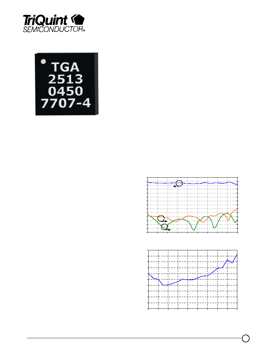
Measured Performance
Bias Conditions: Vd = 5 V, Idq =75 mA, Vg2 = 2V
-21
-18
-15
-12
-9
-6
-3
0
3
6
9
12
15
18
21
2
4
6
8
10
12
14
16
18
20
Frequency (GHz)
G
a
i
n
(dB)
-28
-24
-20
-16
-12
-8
-4
0
4
8
12
16
20
24
28
Re
tur
n
Los
s
(dB)
Gain
Input
Output
0
0.5
1
1.5
2
2.5
3
3.5
4
4.5
5
2
4
6
8
10
12
14
16
18
20
Frequency (GHz)
Nois
e
Figure
(
d
B)

Advance Product Information
January 19, 2006
2
TriQuint Semiconductor Texas: Phone (972)994-8465 Fax (972)994-8504 Email: Info-mmw@tqs.com Web: www.triquint.com
TGA2513-SM
TABLE I
MAXIMUM RATINGS 1/
SYMBOL
PARAMETER
VALUE
NOTES
V
+
Positive Supply Voltage
7 V
2/
V
g1
Gate 1 Supply Voltage Range
-2V TO 0 V
V
g2
Gate 2 Supply Voltage Range
-0.5 V TO +3.5 V
I
+
Positive Supply Current
151 mA
2/
| I
G
|
Gate Supply Current
10 mA
P
IN
Input Continuous Wave Power
21 dBm
2/
P
D
Power Dissipation
See note 3
2/, 3/
T
CH
Operating Channel Temperature
117
°
C
4/, 5/
T
M
Mounting Temperature (30 Seconds)
260
°
C
T
STG
Storage Temperature
-65 to 117
°
C
1/
These ratings represent the maximum operable values for this device.
2/
Current is defined under no RF drive conditions. Combinations of supply voltage, supply
current, input power, and output power shall not exceed P
D
.
3/ For a median life time of 1E+6 hrs, Power dissipation is limited to:
PD(max) = (117
°
C TBASE
°
C) / 32 (
°
C/W)
4/
Junction operating temperature will directly affect the device median time to failure (T
M
). For
maximum life, it is recommended that junction temperatures be maintained at the lowest
possible levels.
5/
These ratings apply to each individual FET.
Advance Product Information
January 19, 2006
3
TriQuint Semiconductor Texas: Phone (972)994-8465 Fax (972)994-8504 Email: Info-mmw@tqs.com Web: www.triquint.com
TABLE III
THERMAL INFORMATION
Parameter
Test Conditions
T
CH
(
o
C)
T
JC
(
q
C/W)
T
M
(HRS)
JC
Thermal Resistance
(channel to backside of
carrier)
Vd = 5 V
I
D
= 75 mA
Pdiss = 0.375 W
97
32
8.1 E+6
Note: Worst case condition with no RF applied, 100% of DC power is
dissipated. Package temperature @ 85
°
C
TABLE II
RF CHARACTERIZATION TABLE
(T
A
= 25
°
C, Nominal)
Vd = 5V, Id = 75 mA Vg2 = 2V Vg1 = ~ -60 mV
SYMBOL
PARAMETER
TEST
CONDITION
NOMINAL
UNITS
Gain
Small Signal Gain
f = 2-20 GHz
17
dB
IRL
Input Return Loss
f = 2-20 GHz
12
dB
ORL
Output Return Loss
f = 2-20 GHz
10
dB
NF
Noise Figure
f = 2-20 GHz
3
dB
P
1dB
Output Power @
1dB Gain
Compression
f = 2-20 GHz
16
dBm
TGA2513-SM
Advance Product Information
January 19, 2006
4
TriQuint Semiconductor Texas: Phone (972)994-8465 Fax (972)994-8504 Email: Info-mmw@tqs.com Web: www.triquint.com
-21
-18
-15
-12
-9
-6
-3
0
3
6
9
12
15
18
21
0
2
4
6
8
10
12
14
16
18
20
22
24
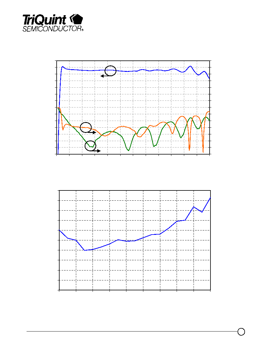
Frequency (GHz)
Gain (dB)
-28
-24
-20
-16
-12
-8
-4
0
4
8
12
16
20
24
28
Return Loss (dB)
Gain
Input
Output
0
0.5
1
1.5
2
2.5
3
3.5
4
4.5
5
2
4
6
8
10
12
14
16
18
20
Frequency (GHz)
Noise Figure (dB)
Measured Performance
Bias Conditions: Vd = 5 V, Idq =75 mA, Vg2 = 2V, Vg1 = ~-60mV, typical
TGA2513-SM
Advance Product Information
January 19, 2006
5
TriQuint Semiconductor Texas: Phone (972)994-8465 Fax (972)994-8504 Email: Info-mmw@tqs.com Web: www.triquint.com
TGA2513-SM
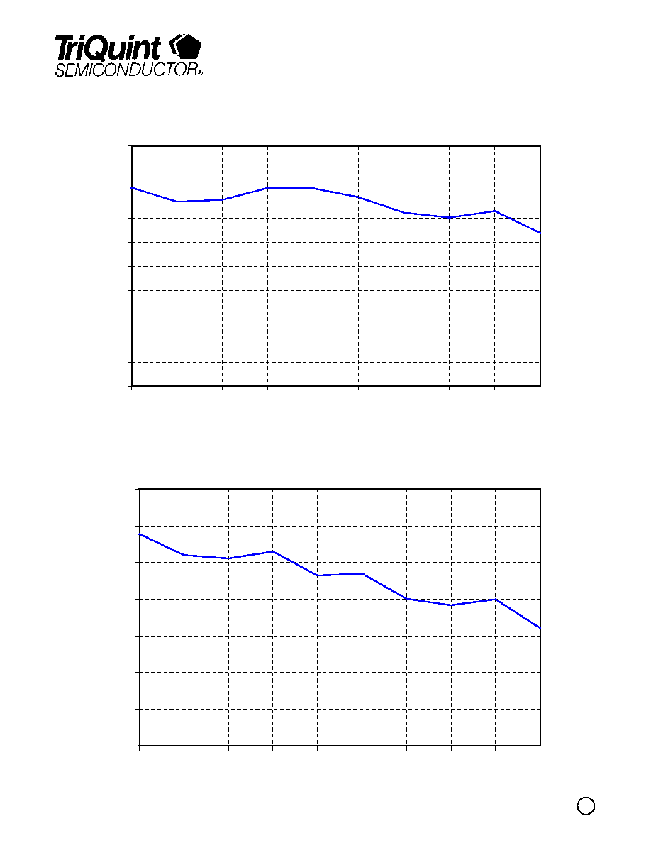
Measured Performance
Bias Conditions: Vd = 5 V, Idq =75 mA, Vg2 = 2V, Vg1 = ~-60mV, typical
16
18
20
22
24
26
28
30
2
4
6
8
10
12
14
16
18
20
Frequency(GHz)
Output TOI dB
m
)
0
2
4
6
8
10
12
14
16
18
20
2
4
6
8
10
12
14
16
18
20
Frequency(GHz)
P
1dB
(dB
m
)

Advance Product Information
January 19, 2006
6
TriQuint Semiconductor Texas: Phone (972)994-8465 Fax (972)994-8504 Email: Info-mmw@tqs.com Web: www.triquint.com
Measured Performance *
Bias Conditions: Vd = 5 V, Idq =75 mA, Vg2 = 2V, Vg1 = ~-60mV, typical
* Note:
Measured data is taken using connectorized evaluation boards. The reference plane is
at RF connectors, and hence connector and board loss has not been de-embedded.
-27
-24
-21
-18
-15
-12
-9
-6
-3
0
0
2
4
6
8
10
12
14
16
18
20
22
24
Frequency (GHz)
I
nput
R
e
t
urn Loss (
d
B
)
-40 deg C
25 deg C
0 deg C
+25 deg C
+50 deg C
+75 deg C
-22
-20
-18
-16
-14
-12
-10
-8
-6
-4
-2
0
0
2
4
6
8
10
12
14
16
18
20
22
24
Frequency (GHz)
Out
put
R
e
t
u
rn Loss (
d
B
)
-40 deg C
-25 deg C
0 deg C
+25 deg C
+50 deg C
+75 deg C
0
2
4
6
8
10
12
14
16
18
20
0
2
4
6
8
10
12
14
16
18
20
22
24
Frequency (GHz)
Ga
in
(d
B)
-40 deg C
-25 deg C
0 deg C
+25 deg C
+50 deg C
+75 deg C
TGA2513-SM

Advance Product Information
January 19, 2006
7
TriQuint Semiconductor Texas: Phone (972)994-8465 Fax (972)994-8504 Email: Info-mmw@tqs.com Web: www.triquint.com
TGA2513-SM
Package Pinout Diagram
; PP
*URXQG 3DG
Pin
Description
1, 3, 4, 5, 7, 8, 10, 13
Ground
2
RF Input
6
Vg1
9
RF Output
11
Vd
12
Vg2
TGA
2513
Date Code
Lot Code
Bottom View
Top View
Dot indicates Pin 1

Advance Product Information
January 19, 2006
8
TriQuint Semiconductor Texas: Phone (972)994-8465 Fax (972)994-8504 Email: Info-mmw@tqs.com Web: www.triquint.com
TGA2513-SM
Mechanical Drawing
GaAs MMIC devices are susceptible to damage from Electrostatic Discharge. Proper precautions should
be observed during handling, assembly and test.
%RWWRP 9LHZ
7ROHUDQFH
8QLWV PP
[ PP
*URXQG 3DG

Advance Product Information
January 19, 2006
9
TriQuint Semiconductor Texas: Phone (972)994-8465 Fax (972)994-8504 Email: Info-mmw@tqs.com Web: www.triquint.com
Recommended Board Layout Assembly *
TGA2513-SM
GaAs MMIC devices are susceptible to damage from Electrostatic Discharge. Proper precautions should
be observed during handling, assembly and test.
* The layout is a general purpose drawing that needs to be tuned for the specific application.
PCB is RO4003 8 mil thickness, 0.5 oz standard copper cladding, with Er = 3.38.
5
:
1
P
F
5) ,1
5) 287
5
:
1
P
F
Vg (Vg1)= ~-
60mV
to obtain 75mA
drain current
Vc (Vg2) = 2V
Vd = 5V
100pF
100pF
Recommended Bias-up Procedure
·
Ensure no RF power is applied to the device
·
Pinch-off device by setting Vg (Vg1) to -1.5V
·
Increase Vd to 5V while monitoring gate current
·
Increase Vc (Vg2) to 2V
·
Increase Vg (Vg1) until drain current reaches 75 mA
·
Apply RF Power
Recommended Bias-Down Procedure
·
Turn off RF power
·
Decrease Vg (Vg1) to -1.5V
·
Decrease Vc (Vg2) to 0 V
·
Decrease Vd to 0 V

Advance Product Information
January 19, 2006
10
TriQuint Semiconductor Texas: Phone (972)994-8465 Fax (972)994-8504 Email: Info-mmw@tqs.com Web: www.triquint.com
Ordering Information
Part
Package Style
TGA2513-SM
QFN 12L 4x4 Surface Mount
Recommended Surface Mount Package Assembly
Proper ESD precautions must be followed while handling packages.
Clean the board with acetone. Rinse with alcohol. Allow the circuit to fully dry.
TriQuint recommends using a conductive solder paste for attachment. Follow solder paste and reflow oven
vendors' recommendations when developing a solder reflow profile. Typical solder reflow profiles are listed
in the table below.
Hand soldering is not recommended. Solder paste can be applied using a stencil printer or dot placement.
The volume of solder paste depends on PCB and component layout and should be well controlled to
ensure consistent mechanical and electrical performance.
Clean the assembly with alcohol.
GaAs MMIC devices are susceptible to damage from Electrostatic Discharge. Proper precautions should
be observed during handling, assembly and test.
Typical Solder Reflow Profiles
Reflow Profile
SnPb
Pb Free
Ramp-up Rate
3
°
C/sec
3
°
C/sec
Activation Time and
Temperature
60 120 sec @ 140 160
°
C
60 180 sec @ 150 200
°
C
Time above Melting Point
60 150 sec
60 150 sec
Max Peak Temperature
240
°
C
260
°
C
Time within 5
°
C of Peak
Temperature
10 20 sec
10 20 sec
Ramp-down Rate
4 6
°
C/sec
4 6
°
C/sec
TGA2513-SM