Advance Product Information
September 15, 2004
1
Note: Devices designated as EPU are typically early in their characterization process prior to finalizing all electrical and process
specifications. Specifications are subject to change without notice.
TriQuint Semiconductor Texas Phone: (972)994-8465 Fax: (972)994-8504 Email: info-mmw@tqs.com Web: www.triquint.com
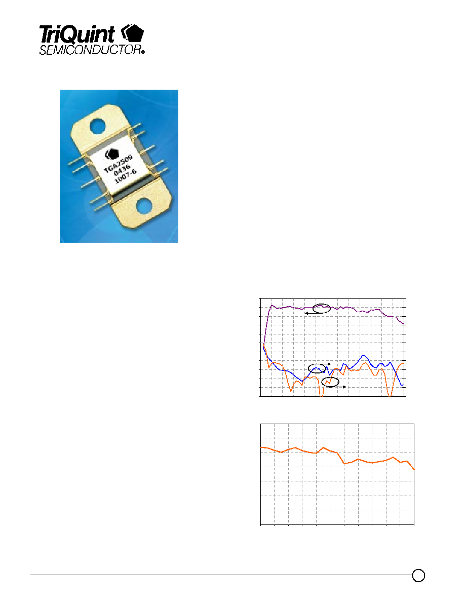
Wideband Packaged HPA with AGC TGA2509-EPU-FL
LOT CODE
Key Features
·
Frequency Range: 2-20 GHz
·
29 dBm Nominal P1dB
·
15 dB Nominal Gain, Midband
·
25dB AGC Range
·
10 lead flange package style
·
Bias Conditions: Vd = 12 V, Idq = 1.1 A
·
Package Dimensions: 0.7 x 0.3 x 0.1 in.
Primary Applications
·
Wideband Power Amp
·
Military EW and ECM
·
Test Equipment
·
VSAT and Digital Radio
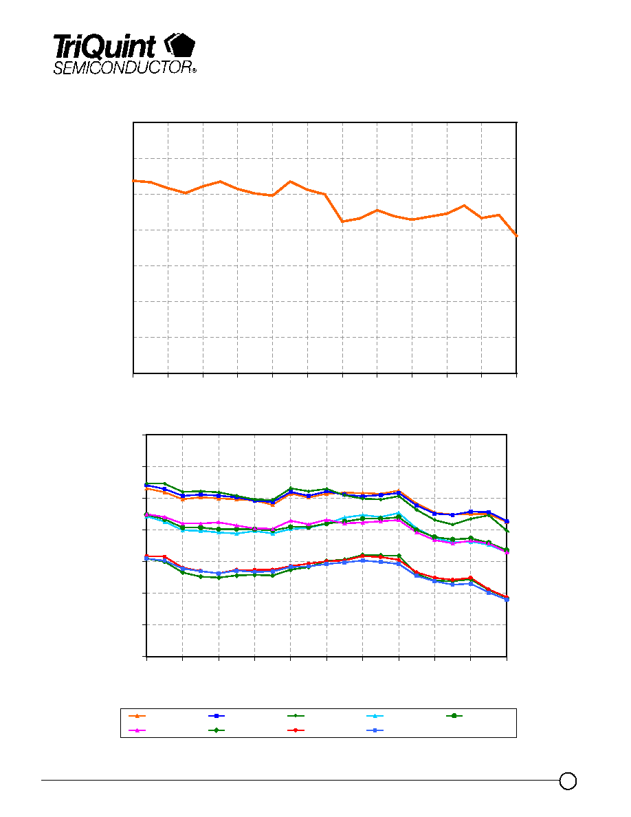
Measured Fixtured Data
Bias Conditions: Vd =12 V, Id= 1.1 A
Product Description
The TriQuint TGA2509-EPU-FL is a
Wideband High Power Amplifier with 25 dB
AGC range. The HPA operates from 2-20
GHz and provides 29dBm of output power at
1 dB gain compression with small signal gain
of 15 dB.
The TGA2509-EPU-FL is suitable for a
variety of applications such as wideband
electronic warfare systems, test equipment
and VSAT and Digital Radio. The flange lead
package has a high thermal conductivity
copper alloy base.
Evaluation Boards are available.
-24
-20
-16
-12
-8
-4
0
4
8
12
16
20
0
2
4
6
8
10
12
14
16
18
20
22
24
26
Frequency (GHz)
G
a
in
(
d
B
)
-24
-20
-16
-12
-8
-4
0
4
8
12
16
20
Retu
rn
L
o
ss (d
B)
Gain
Input
Output
20
22
24
26
28
30
32
34
2
4
6
8
10
12
14
16
18
20
22
24
Frequency (GHz)
Out
put
P
o
wer (
d
B
m
)
Advance Product Information
September 15, 2004
2
Note: Devices designated as EPU are typically early in their characterization process prior to finalizing all electrical and process
specifications. Specifications are subject to change without notice.
TriQuint Semiconductor Texas Phone: (972)994-8465 Fax: (972)994-8504 Email: info-mmw@tqs.com Web: www.triquint.com
TGA2509-EPU-FL
TABLE I
MAXIMUM RATINGS 1/
SYMBOL
PARAMETER
VALUE
NOTES
V
+
Positive Supply Voltage
12.5 V
2/
V
g1
Gate 1 Supply Voltage Range
-2V TO 0 V
V
g2
Gate 2 Supply Voltage Range
-2V TO 0 V
V
c
AGC Control Voltage Range
V
c
< +5 V
V
+
V
c
< 14V
I
+
Positive Supply Current
1.4 A
2/
| I
G
|
Gate Supply Current
70 mA
P
IN
Input Continuous Wave Power
30 dBm
2/
P
D
Power Dissipation (without using AGC)
13.2 W
2/, 3/
P
D
Power Dissipation (when Vc < +2V)
10.6 W
2/, 3/
T
CH
Operating Channel Temperature
150
°
C
4/, 5/
T
M
Mounting Temperature (30 Seconds)
210
°
C
T
STG
Storage Temperature
-65 to 150
°
C
1/
These ratings represent the maximum operable values for this device.
2/
Current is defined under no RF drive conditions. Combinations of supply voltage, supply
current, input power, and output power shall not exceed P
D
.
3/
When operated at this power dissipation with a base plate temperature of 60
°
C, the median
life is 1 E+6 hours.
4/
Junction operating temperature will directly affect the device median time to failure (T
M
). For
maximum life, it is recommended that junction temperatures be maintained at the lowest
possible levels.
5/
These ratings apply to each individual FET.

Advance Product Information
September 15, 2004
3
Note: Devices designated as EPU are typically early in their characterization process prior to finalizing all electrical and process
specifications. Specifications are subject to change without notice.
TriQuint Semiconductor Texas Phone: (972)994-8465 Fax: (972)994-8504 Email: info-mmw@tqs.com Web: www.triquint.com
TABLE II
RF CHARACTERIZATION TABLE
(T
A
= 25
°
C, Nominal)
Vd = 12 V, Id = 1.08 A
SYMBOL
PARAMETER
TEST
CONDITION
NOMINAL
UNITS
Gain
Small Signal Gain
f = 2-20 GHz
15
dB
IRL
Input Return Loss
f = 2-20 GHz
10
dB
ORL
Output Return Loss
f = 2-20 GHz
12
dB
P
1dB
Output Power @
1dB Gain
Compression
f = 2-20 GHz
29
dBm
TABLE III
THERMAL INFORMATION
Parameter
Test Conditions
T
CH
(
o
C)
R
T
JC
(
q
C/W)
T
M
(HRS)
R
JC
Thermal
Resistance
(channel to backside
of package)
Vd = 12 V
I
D
= 1.08 A
Pdiss = 13.2 W
(without using AGC)
150
6.4
1 E+6
R
JC
Thermal
Resistance
(channel to backside
of package)
Vd = 12 V
I
D
= 0.88 A
Pdiss = 10.6 W
(when using AGC)
150
8.3
1 E+6
Note: Package attached with mounting hardware and metal shim (Al or In) to
carrier at 65
°
C baseplate temperature. Worst case is at saturated output power
when DC power consumption rises to 15 W with 1 W RF power delivered to load.
Power dissipated is 14 W and the temperature rise in the channel is 90
°
C.
Baseplate temperature must be reduced to 60
°
C to remain below the 150
°
C
maximum channel temperature.
TGA2509-EPU-FL
Advance Product Information
September 15, 2004
4
Note: Devices designated as EPU are typically early in their characterization process prior to finalizing all electrical and process
specifications. Specifications are subject to change without notice.
TriQuint Semiconductor Texas Phone: (972)994-8465 Fax: (972)994-8504 Email: info-mmw@tqs.com Web: www.triquint.com
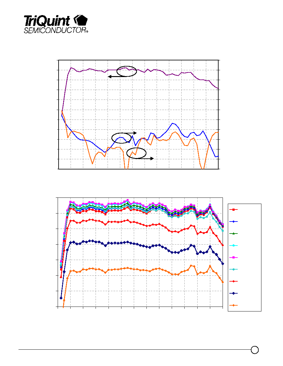
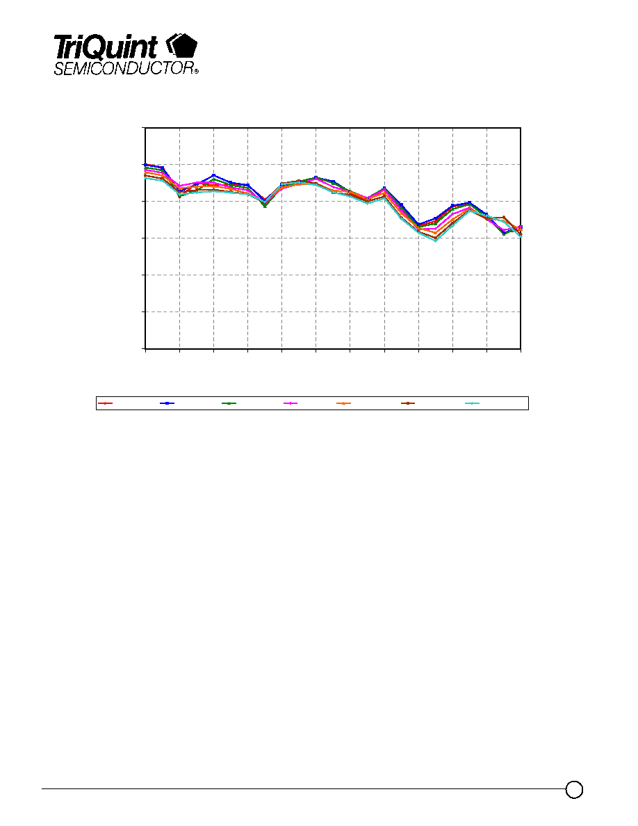
Typical Fixtured Performance
Bias Conditions: Vd = 12V, Id = 1.08A, Vg1 = -0.28V Typical, Vg2 = -0.35V Typical, Vc (optional) = 2.6V Typical
-15
-10
-5
0
5
10
15
20
0
2
4
6
8
10
12
14
16
18
20
22
24
26
Frequency (GHz)
Ga
in (dB)
Vc=2.6v
Vc=2.0v
Vc=1.5v
Vc=1.0v
Vc=0.5v
Vc=0v
Vc=-0.25v
Vc=-0.50v
Vc=-0.75v
-24
-20
-16
-12
-8
-4
0
4
8
12
16
20
0
2
4
6
8
10
12
14
16
18
20
22
24
26
Frequency (GHz)
Gain (dB)
-24
-20
-16
-12
-8
-4
0
4
8
12
16
20
Return Loss (dB)
Gain
Input
Output
TGA2509-EPU-FL
Advance Product Information
September 15, 2004
5
Note: Devices designated as EPU are typically early in their characterization process prior to finalizing all electrical and process
specifications. Specifications are subject to change without notice.
TriQuint Semiconductor Texas Phone: (972)994-8465 Fax: (972)994-8504 Email: info-mmw@tqs.com Web: www.triquint.com
TGA2509-EPU-FL
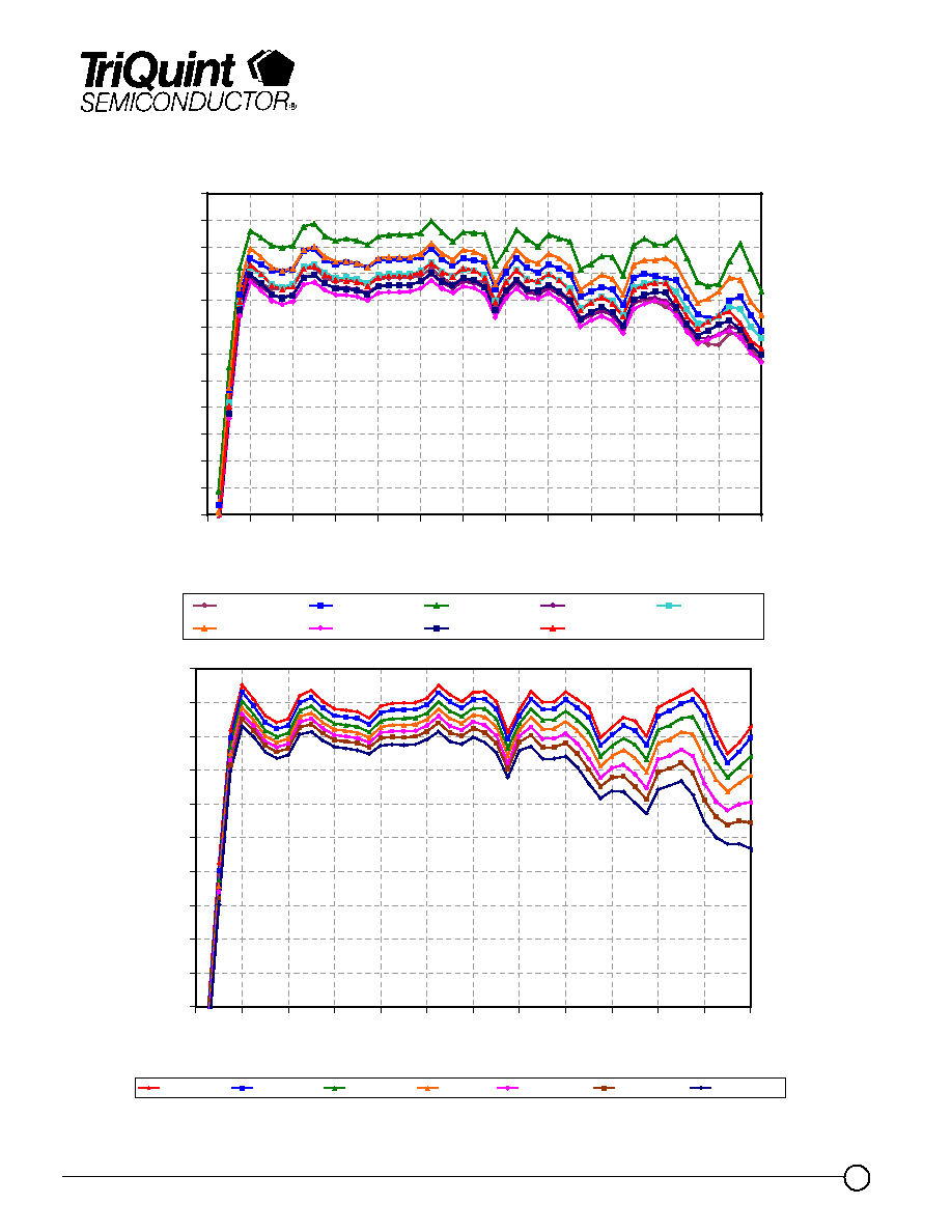
Typical Fixtured Performance
Bias Conditions: Vd = 12V, Id = 1.08A, Vg1 = -0.28V Typical, Vg2 = -0.35V Typical, Vc (optional) = 2.6V Typical
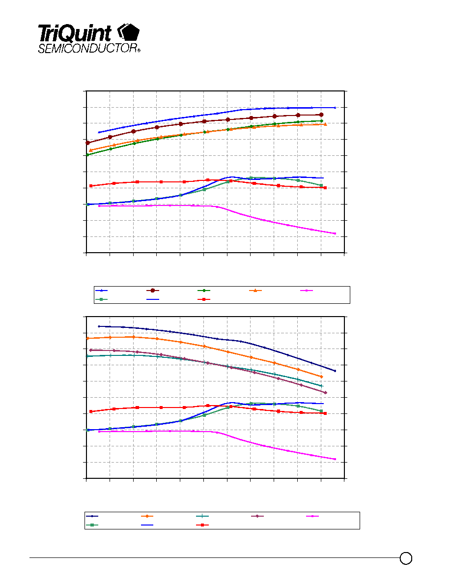
0
2
4
6
8
10
12
14
16
18
20
22
24
0
2
4
6
8
10
12
14
16
18
20
22
24
26
Frequency (GHz)
Gain (dB)
5v600mA
5v800mA
5v1000mA
7v600mA
7v800mA
7v1000mA
9v600mA
9v800mA
9v1000mA
0
2
4
6
8
10
12
14
16
18
20
0
2
4
6
8
10
12
14
16
18
20
22
24
Frequency (GHz)
Ga
in
(d
B)
-55 deg-C
-40 deg-C
-20 deg-C
0 deg-C
+25 deg-C
+45 deg-C
+65 deg-C
Advance Product Information
September 15, 2004
6
Note: Devices designated as EPU are typically early in their characterization process prior to finalizing all electrical and process
specifications. Specifications are subject to change without notice.
TriQuint Semiconductor Texas Phone: (972)994-8465 Fax: (972)994-8504 Email: info-mmw@tqs.com Web: www.triquint.com
Typical Fixtured Performance
Bias Conditions: Vd = 12V, Id = 1.08A, Vg1 = -0.28V Typical, Vg2 = -0.35V Typical, Vc (optional) = 2.6V Typical
18
20
22
24
26
28
30
32
2
4
6
8
10
12
14
16
18
20
22
Frequency (GHz)
Output Power@ P1dB (dBm)
9v1000ma
9v800ma
9v600ma
7v1000ma
7v800ma
7v600ma
5v1000ma
5v800ma
5v600ma
TGA2509-EPU-FL
20
22
24
26
28
30
32
34
2
4
6
8
10
12
14
16
18
20
22
24
Frequency (GHz)
Output Power @ P1dB (dBm)
Advance Product Information
September 15, 2004
7
Note: Devices designated as EPU are typically early in their characterization process prior to finalizing all electrical and process
specifications. Specifications are subject to change without notice.
TriQuint Semiconductor Texas Phone: (972)994-8465 Fax: (972)994-8504 Email: info-mmw@tqs.com Web: www.triquint.com
Typical Fixtured Performance
Bias Conditions: Vd = 12V, Id = 1.08A, Vg1 = -0.28V Typical, Vg2 = -0.35V Typical, Vc (optional) = 2.6V Typical
20
22
24
26
28
30
32
2
4
6
8
10
12
14
16
18
20
22
24
Frequency (GHz)
Ou
tp
u
t
Po
wer @ P1d
B
(d
Bm)
-50 deg-C
-40 deg-C
-20 deg-C
0 deg-C
+25 deg-C
+45 deg-C
+65 deg-C
TGA2509-EPU-FL
Advance Product Information
September 15, 2004
8
Note: Devices designated as EPU are typically early in their characterization process prior to finalizing all electrical and process
specifications. Specifications are subject to change without notice.
TriQuint Semiconductor Texas Phone: (972)994-8465 Fax: (972)994-8504 Email: info-mmw@tqs.com Web: www.triquint.com
0
2
4
6
8
10
12
14
16
18
20
8
9
10
11
12
13
14
15
16
17
18
19
Pin (dBm)
G
a
in (dB)
700
800
900
1000
1100
1200
1300
1400
1500
1600
1700
IDS
(m
A)
2GHz Gain
8GHz_Gain
14_GHz_Gain
20GHz_Gain
2GHz_Id
8GHz_Id
14GHz_Id
20GHz_Id
5
8
11
14
17
20
23
26
29
32
35
8
9
10
11
12
13
14
15
16
17
18
19
Pin (dBm)
Output Power (dBm)
700
800
900
1000
1100
1200
1300
1400
1500
1600
1700
IDS
(m
A)
2GHz_Pout
8GHz_Pout
14GHz_Pout
20GHz_Pout
2GHz_Id
8GHz_Id
14GHz_Id
20GHz_Id
Typical Fixtured Performance
Bias Conditions: Vd = 12V, Id = 1.08A, Vg1 = -0.28V Typical, Vg2 = -0.35V Typical, Vc (optional) = 2.6V Typical
TGA2509-EPU-FL

Advance Product Information
September 15, 2004
9
Note: Devices designated as EPU are typically early in their characterization process prior to finalizing all electrical and process
specifications. Specifications are subject to change without notice.
TriQuint Semiconductor Texas Phone: (972)994-8465 Fax: (972)994-8504 Email: info-mmw@tqs.com Web: www.triquint.com
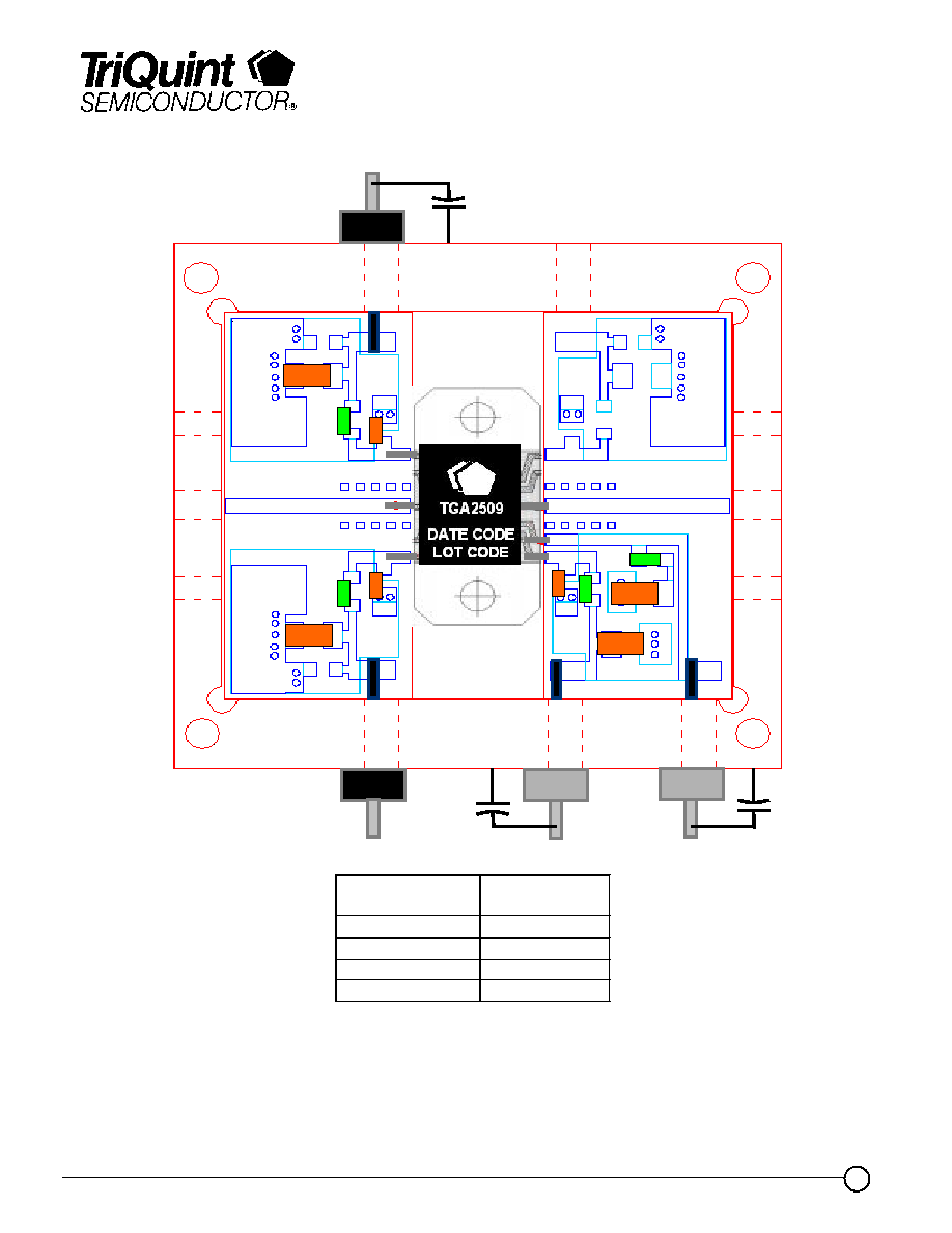
Package Dimensional Drawing
TGA2509-EPU-FL
Note: Units are in inches.
Package size tolerance ± 0.005 in.
I8
W8
SAĂPVU
SAĂDI
(
'
&
%
$
#
"
!
WB
WB!
I8
W9
I8
I8
$
'$
$ $
%$
&
% $
'$
(ĂYĂ!
Ă$!
#!
!$
&'
"$
$
#$
!$
!
ĂĂ
ĹĂĂ ĹĂ Ĺ
G@69ĂXD9UCĂ6I9ĂG@IBUCĂ
GaAs MMIC devices are susceptible to damage from Electrostatic Discharge. Proper precautions should
be observed during handling, assembly and test.
Advance Product Information
September 15, 2004
10
Note: Devices designated as EPU are typically early in their characterization process prior to finalizing all electrical and process
specifications. Specifications are subject to change without notice.
TriQuint Semiconductor Texas Phone: (972)994-8465 Fax: (972)994-8504 Email: info-mmw@tqs.com Web: www.triquint.com
Evaluation Board Drawing
Vc
Vg1
Vd
Vg2
RF In
RF Out
GaAs MMIC devices are susceptible to damage from Electrostatic Discharge. Proper precautions should
be observed during handling, assembly and test.
TGA2509-EPU-FL
Bias Procedures:
Vc bias connection is optional, but the 0.1uF cap always needs to be connected.
For biasing without AGC control:
1. Apply -1.2V to Vg1, and -1.2V to Vg2.
2. Apply +12V to Vd.
4. Adjust Vg1 to attain 580 mA drain current (Id)
4. Adjust Vg2 to attain 1080 mA total drain current (Id).
For biasing with AGC control:
1. Apply -1.2V to Vg1 and -1.2V to Vg2
2. Apply +12V to Vd
3. Apply +2.6V to Vc
4. Adjust Vg1 to attain 580 mA drain current (Id)
5. Adjust Vg2 to attain 1080 mA total drain current (Id).
6. Adjust Vc as needed to control gain level.
Advance Product Information
September 15, 2004
11
Note: Devices designated as EPU are typically early in their characterization process prior to finalizing all electrical and process
specifications. Specifications are subject to change without notice.
TriQuint Semiconductor Texas Phone: (972)994-8465 Fax: (972)994-8504 Email: info-mmw@tqs.com Web: www.triquint.com
Typical Evaluation Board Layout *
LOT CODE
DATE CODE
TGA2509
6
4
9
10
1
7 8
5
Vc
Vg2
Vd
Vg1
3
2
11
33uF
33uF
33uF
GaAs MMIC devices are susceptible to damage from Electrostatic Discharge. Proper precautions should
be observed during handling, assembly and test.
TGA2509-EPU-FL
COMPONENT
VALUE
1, 4, 9,10
1 uF
2, 5, 8
10
3, 6, 7
0.01 uF
11
100

Advance Product Information
September 15, 2004
12
Note: Devices designated as EPU are typically early in their characterization process prior to finalizing all electrical and process
specifications. Specifications are subject to change without notice.
TriQuint Semiconductor Texas Phone: (972)994-8465 Fax: (972)994-8504 Email: info-mmw@tqs.com Web: www.triquint.com
Assembly of a TGA2509-EPU Flange Mount Package onto a Motherboard
Manual Assembly for Prototypes
1. Clean the motherboard or the similar module with Acetone. Rinse with alcohol and DI water. Allow the circuit
to fully dry.
2. To improve the thermal and RF performance, TriQuint recommends using two # 0-80 bolts to attach a heat
sink to the bottom of the package with an indium alloy preform, or equivalent, between the two.
3. Apply Tin/Lead solder, or equivalent, to each active pin of the TGA2509.
4 Clean the assembly with alcohol.
Ordering Information
Part
Package Style
TG2509-EPU-FL
Flange (Leads bolted down)
GaAs MMIC devices are susceptible to damage from Electrostatic Discharge. Proper precautions should
be observed during handling, assembly and test.
TGA2509-EPU-FL