
TriQuint Semiconductor Texas : (972)994 8465 Fax (972)994 8504 Web: www.triquint.com
Product Data Sheet
1
DC-18GHz MPA with AGC TGA1328-SCC
OC-192 12.5GB/s LN/MZ Driver and Receive AGC Applications
Key Features and Performance
À
0.5um pHEMT Technology
À
DC - 14GHz Linear Bandwidth
À
DC -18GHz Saturated Power BW
À
16dB Small Signal Gain
À
6dB AGC Range
À
20ps Edge Rates (20/80)
À
8Vpp 12.5Gb/s NRZ PRBS
À
Low power dissipation
À
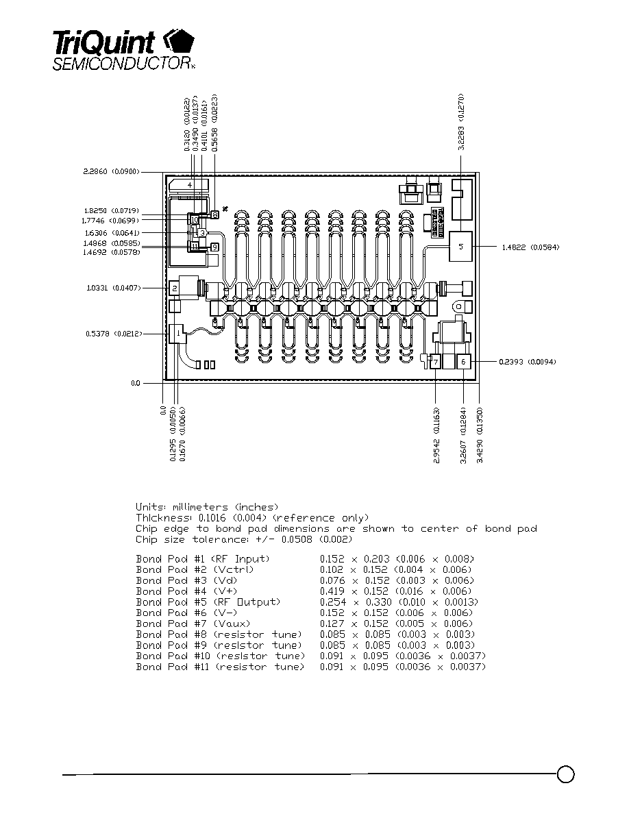
Chip Dimensions 3.4mm x 2.3mm
Primary Applications
À
12.5GBit OC192 LN/MZ Driver
À
12.5GBit OC192 AGC Receive
Description
The TriQuint TGA1328-SCC is a medium power
wideband AGC amplifier that typically provides 12dB
saturated gain with 6dB AGC range. Typical input and
output return loss is >10dB. Typical Noise Figure is
2.5dB at 3GHz. Minimum saturated output power is
25dBm. Small signal BW is near 14GHz with saturated
power performance to 18GHz. RF ports are DC coupled
enabling the user to customize system corner
frequencies.
The TGA1328-SCC is an excellent choice for 9.9, 10.7,
and 12.5Gb/s NRZ applications driving a Lithium Niobate
Optical Modulator with electrical Non-Return-to-Zero
(NRZ) data. In addition it may be used as a receive AGC
amplifier.
Drain bias may be applied thru the on-chip drain
termination resistor for low drive applications or thru the
RF output port for high drive applications.
The TGA1328-SCC requires off-chip decoupling and
blocking components. Each device is 100% DC and RF
tested on-wafer to ensure performance compliance.
The TGA1328SCC is available in chip form or assembled
into a surface mount package (see the TGA8652-EPU
data sheet for more information on the SMT package).
March 19, 2002
12.5 Gb/s eye: 8V(amp) **
Measured 12.5Gb/s Performance
** Input 12.5Gb/s data stream generated
using an Anritsu PPG (Vin=2Vpp).
12.5Gb/s NRZ 2^31-1
Single Stage
TriQuint Semiconductor Texas : (972)994 8465 Fax (972)994 8504 Web: www.triquint.com
Product Data Sheet
2
SYMBOL
PARAMETER 6/
VALUE
NOTES
V
+
Vd(FET)
POSITIVE SUPPLY VOLTAGE
Biased thru On-chip Drain Termination
Biased thru the RF Output Port using a Bias Tee
12 V
10 V
I
+
Id
POSITIVE SUPPLY CURRENT
Biased thru On-chip Drain Termination
Biased thru the RF Output Port using a Bias Tee
110 mA
250 mA
1/
P
d
POWER DISSIPATION
2.25 W
2/
Vg
Ig
NEGATIVE GATE
Voltage
Gate Current
0V to -3V
5 mA
Vctl
Ictl
CONTROL GATE
Voltage
Gate Current
Vd/2 to -3V
5 mA
3/
P
IN
V
IN
RF INPUT
Sinusoidal Continuous Wave Power
12.5Gb/s PRBS Input Voltage Peak to Peak
23 dBm
5 Vpp
T
CH
OPERATING CHANNEL TEMPERATURE
150
0
C
4/ 5/
T
M
MOUNTING TEMPERATURE
(30 SECONDS)
320
0
C
T
STG
STORAGE TEMPERATURE
-65 to 150
0
C
TGA1328-SCC
Notes:
1/ Assure that the combination of Vd and Id does not exceed the maximum power dissipation rating.
2/ When operated at this bias condition with a base plate temperature of 70
0
C, the median life is reduced
from >1E8 to 2.4E6 hours.
3/ Assure that Vctl never exceeds Vd during bias up and down sequences. Also, assure that Vctl never exceeds
1.5V during normal operation.
4/ These ratings apply to each individual FET.
5/ Junction operating temperature will directly affect the device median time to failure (MTTF). For maximum
life, it is recommended that junction temperatures be maintained at the lowest possible levels.
6/ These ratings represent the maximum operable values for the device.
MAXIMUM RATINGS
TriQuint Semiconductor Texas : (972)994 8465 Fax (972)994 8504 Web: www.triquint.com
Product Data Sheet
3
Parameter
Test Condition
P
diss
(W)
T
Base
(
░
C)
T
CH
(
░
C)
R
JC
(
░
C/W)
MTTF
(HRS)
Vd(FET)=6.5V, Vctl=1V
Id=170mA +/-5%
1.1
70
103
30
>1E7
R
JC
Thermal Resistance
(channel to backside of carrier)
V+ = 8 V**, V
ctrl
= 1.5 V,
Id = 80 mA
▒
5%
0.36
70
80
29
>1E8
THERMAL INFORMATION*
DC SPECIFICATIONS (100%)
(T
A
= 25
░
C + 5
░
C)
Notes:
* Based on a detailed thermal model. Assumes worst case power dissipation condition
where no RF is applied at the input (no power is dissipated in the load).
** When applying drain bias at V+, several volts are dropped across the internal drain
terminations resistor (between V+ and Vd). For Id=80mA, approximately 3.5V is dropped
across the drain termination resistor making Vd(FET)=4.5V. Total power dissipation in
the FET is .36 watts.
TGA1328-SCC
NOTES
SYMBOL
TEST CONDITIONS
LIMITS
UNITS
2/
MIN
MAX
I
DSS
STD
110
516
mA
I
MAX
STD
Infor. only
Infor. only
mA
Gm
STD
241
581
mS
1/
|V
P1
|
STD
0.5
1.5
V
1/
|V
P2
|
STD
0.5
1.5
V
1/
|V
BVGD
|
STD
13
30
V
1/
|V
BVGS
|
STD
13
30
V
R1,2
STD
30
45
Ohm
R4
STD
35
56
Ohm
1/
V
P
, V
BVGD
, and V
BVGS
are negative.
2/
The measurement conditions are subject to change at the manufacture's discretion

TriQuint Semiconductor Texas : (972)994 8465 Fax (972)994 8504 Web: www.triquint.com
Product Data Sheet
4
TGA1328-SCC
RF SPECIFICATIONS
(T
A
= 25
░
C + 5
░
C)
NOTE
TEST
MEASUREMENT
CONDITIONS
VALUE
UNITS
MIN
TYP
MAX
3dB BANDWIDTH
14
GHz
SATURATED POWER BW
18
GHz
1/, 2/
SMALL-SIGNAL
GAIN MAGNITUDE
2 and 4 GHz
6 GHz
10 GHz
14 GHz
18 GHz
16
15
14
13
11
dB
SMALL SIGNAL AGC RANGE
Midband
6
dB
NOISE FIGURE
3GHz
2.5
dB
SATURATED OUTPUT
VOLTAGE (EYE AMPLITUDE)
Vin=2Vpp at
12.5Gb/s PRBS
8
Vpp
1/, 3/
OUTPUT POWER @ PIN =
14dBm
2, 4, and 6 GHz
25
dBm
INPUT RETURN LOSS
MAGNITUDE
DC-10 GHz
-12
dB
OUTPUT RETURN LOSS
MAGNITUDE
DC-10 GHz
-12
dB
ADDITIVE JITTER
< 2
pS
GROUP DELAY
DC-10 GHz
+/- 20
pS
RISE TIME
< 30
pS
Notes:
1/ Verified at RF on-wafer probe.
2/ S21Bias: V+=8V, adjust Vg1 to achieve Id=80mA+/-5%, Vg2=1.5V
Note: Drain bias is applied thru the on-chip drain termination resistor.
3/ Power Bias: Vtee=8V, adjust Vg1 to achieve Id=175mA+/-5%, Vg2=1.5V
Note: Drain bias is applied thru the RF output port using a bias tee, voltage is at the DC input to the bias tee.
TriQuint Semiconductor Texas : (972)994 8465 Fax (972)994 8504 Web: www.triquint.com
Product Data Sheet
5
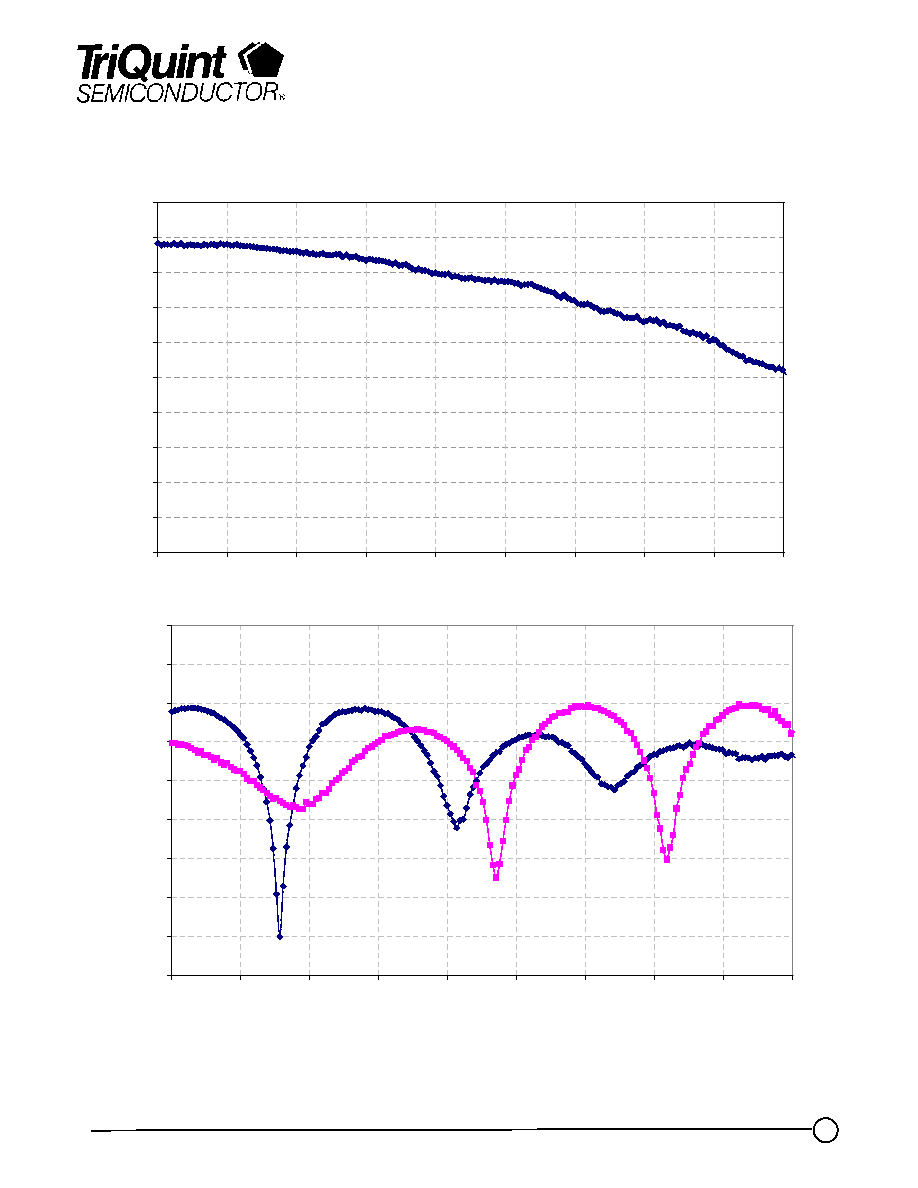
TGA1328-SCC
0
2
4
6
8
10
12
14
16
18
20
2
4
6
8
10
12
14
16
18
20
Frequency (GHz)
S21 (
d
B
)
-45
-40
-35
-30
-25
-20
-15
-10
-5
0
2
4
6
8
10
12
14
16
18
20
Frequency (GHz)
S11 (
d
B
)
an
d
S22 (
d
B
)
s11
s22
TGA1328 Typical Measured S-parameters
TriQuint Semiconductor Texas : (972)994 8465 Fax (972)994 8504 Web: www.triquint.com
Product Data Sheet
6
TGA1328-SCC
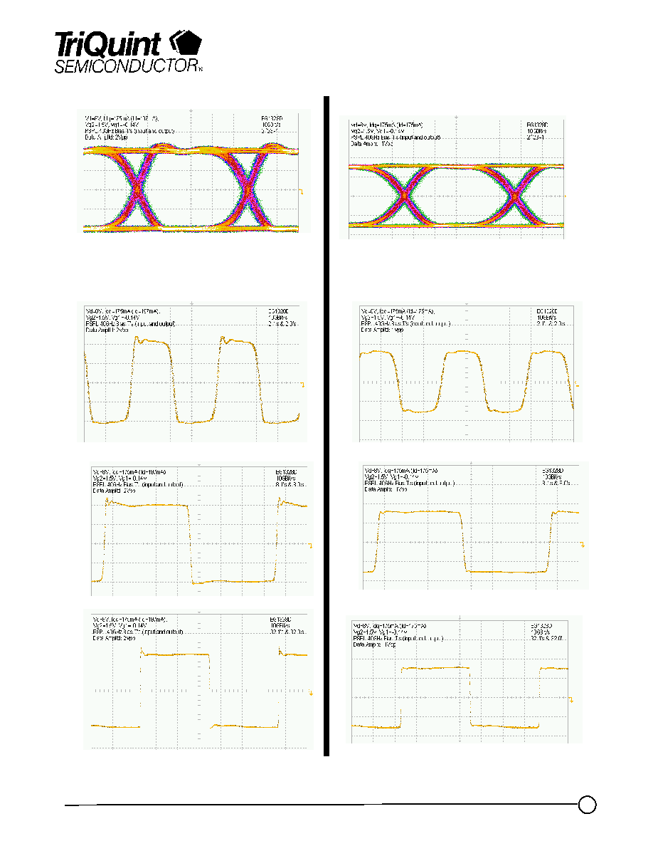
10GBit/s Performance
Output = 8V P-P, Input = 2V P-P
scale 2V/div, 20ps/div
10GBit/s Performance
Output =6V P-P, Input = 1V P-P
scale 2V/div, 20ps/div
Measured Performance
2 1's and 2 0's, 100ps/div
8 1's and 8 0's, 200ps/div
32 1's and 32 0's, 1ns/div
8V P-P (Saturated)
6V P-P (Near Small Signal)
8V P-P
6V P-P
2 1's and 2 0's, 100ps/div
8 1's and 8 0's, 200ps/div
32 1's and 32 0's, 1ns/div
TriQuint Semiconductor Texas : (972)994 8465 Fax (972)994 8504 Web: www.triquint.com
Product Data Sheet
7
TGA1328-SCC
TriQuint Semiconductor Texas : (972)994 8465 Fax (972)994 8504 Web: www.triquint.com
Product Data Sheet
8
TGA1328-SCC
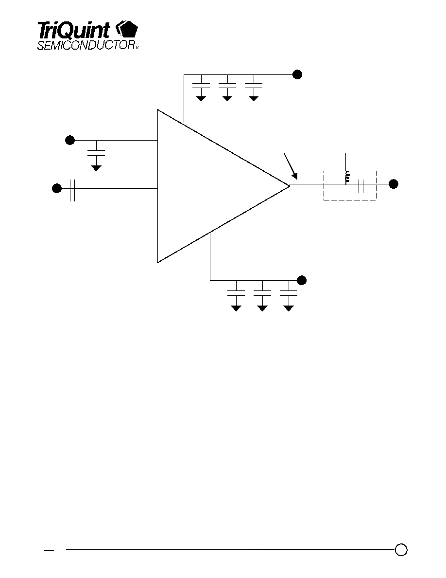
Bias Procedure
1) Make sure no RF power is applied to the device before continuing.
2) Pinch off device by setting Vg to ¡2.5V.
3) Raise Vd to 8.0V while monitoring drain current. Current should be zero.
NOTE: Vd bias should be applied to the RF output port via a bias tee for high power bias.
4) Raise Vctl to 1.0V (no greater than 1.5V).
5) Make Vg more positive until drain current reaches 170mA. (80 mA for low noise bias)
6) Apply RF power. Note Vg supply must be capable of sinking 5mA of current.
1
2
5
4
7
RF in
RFout and Vd
1800pF
0.1uF (2pl)
V+
Vg
1800pF
0.1uF (2pl)
Vctrl
(Vctl)
TGA1328
Note: Drain bias must be applied at Vd
(pin 5) thru broadband bias tee for high
bias mode.
Bypass caps must remain on Pin 4
0.01uF
V(tee)
TriQuint Semiconductor Texas : (972)994 8465 Fax (972)994 8504 Web: www.triquint.com
Product Data Sheet
9
GaAs MMIC devices are susceptible to damage from Electrostatic Discharge. Proper precautions should
be observed during handling, assembly and test.
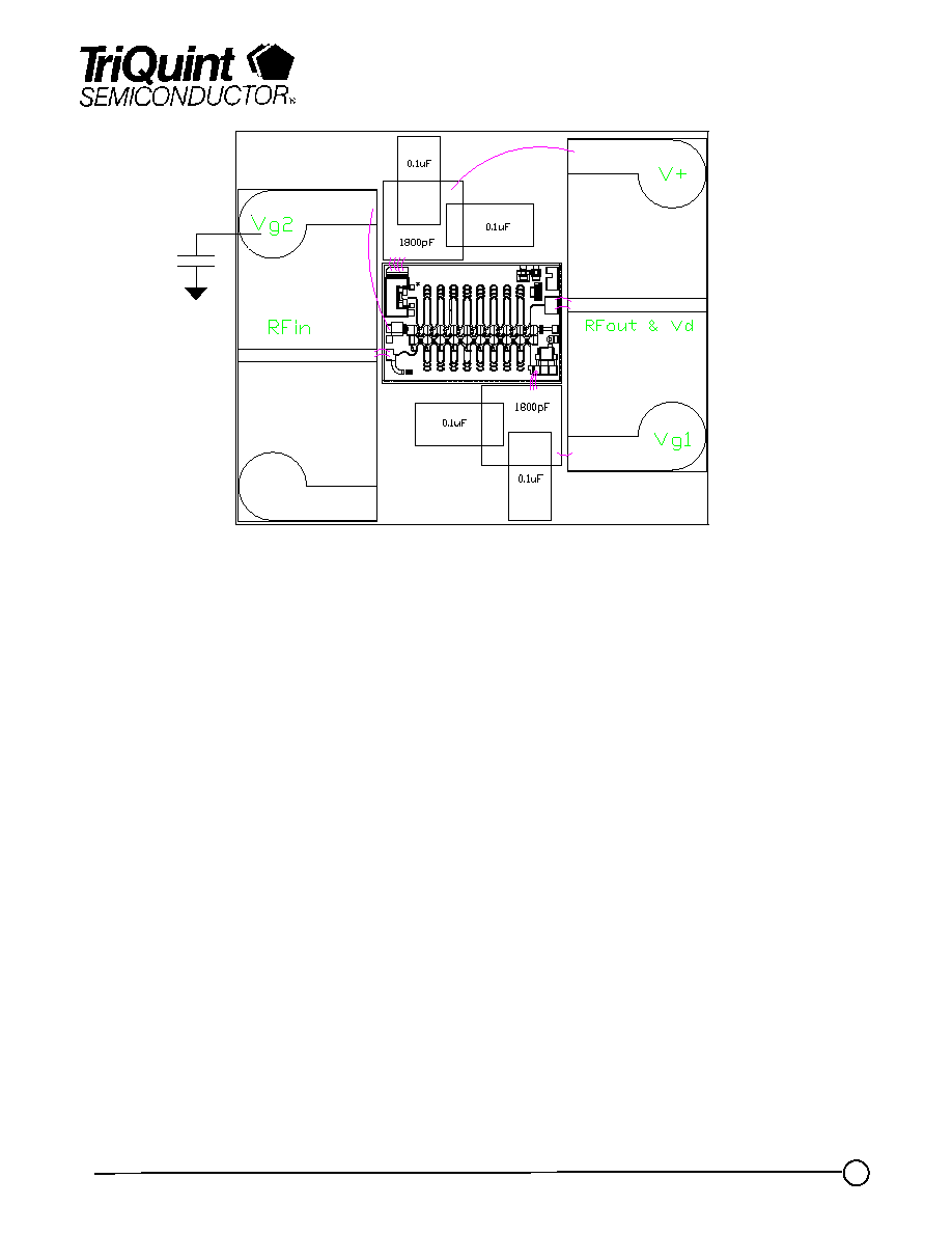
TGA1328-SCC
Recommend additional
0.01uF bypass cap
located on Vctrl supply line
on test fixture
0.01uF
Vctrl
Reflow process assembly notes:
À
Use AuSn (80/20) solder with limited exposure to temperatures at or above 300
ºC.
À
An alloy station or conveyor furnace with reducing atmosphere should be used.
À
No fluxes should be utilized.
À
Coefficient of thermal expansion matching is critical for long-term reliability.
À
Devices must be stored in a dry nitrogen atmosphere.
Component placement and adhesive attachment assembly notes:
À
Vacuum pencils and/or vacuum collets are the preferred method of pick up.
À
Air bridges must be avoided during placement.
À
The force impact is critical during auto placement.
À
Organic attachment can be used in low-power applications.
À
Curing should be done in a convection oven; proper exhaust is a safety concern.
À
Microwave or radiant curing should not be used because of differential heating.
À
Coefficient of thermal expansion matching is critical.
Interconnect process assembly notes:
À
Thermosonic ball bonding is the preferred interconnect technique.
À
Force, time, and ultrasonics are critical parameters.
À
Aluminum wire should not be used.
À
Discrete FET devices with small pad sizes should be bonded with 0.0007-inch wire.
À
Maximum stage temperature is 200
ºC.