TriQuint Semiconductor Texas : Phone (972)994-8465 Fax (972)994 8504 Web: www.triquint.com
Advance Product Information
November 6, 2001
1
Ka Band Wideband LNA/Driver TGA1319C-EPU
Key Features and Performance
À
0.15um pHEMT Technology
À
16-30 GHz Frequency Range
À
2.25 dB Nominal Noise Figure midband
À
21 dB Nominal Gain
À
14 dBm Pout
À
Bias 5V, 60 mA with -0.5V < Vg < +0.5V
Note: Devices designated as EPU are typically early in their characterization process prior to finalizing all electrical and process
specifications. Specifications subject to change without notice
Primary Applications
À
Point-to-Point Radio
À
Point-to-Multipoint Communications
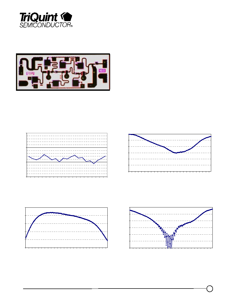
Typical NF @ 25C
Typical Gain @ 25C
Chip Dimensions 2.179 mm x .847 mm
Typical S22 @ 25C
Typical S11 @ 25C
0
5
10
15
20
25
10 11 12 13 14 15 16 17 18 19 20 21 22 23 24 25 26 27 28 29 30 31 32 33 34 35
Frequency ( GHz)
Gain
(d
B)
-30
-25
-20
-15
-10
-5
0
10 11 12 13 14 15 16 17 18 19 20 21 22 23 24 25 26 27 28 29 30 31 32 33 34 35
Frequency ( GHz)
Input
R
L
(
d
B
)
-30
-25
-20
-15
-10
-5
0
10 11 12 13 14 15 16 17 18 19 20 21 22 23 24 25 26 27 28 29 30 31 32 33 34 35
Frequency ( GHz)
O
u
tp
u
t
RL
(d
B)
1 .5
2
2 .5
3
2 1
2 1 . 5
2 2
2 2 . 5
2 3
2 3 . 5
2 4
2 4 . 5
2 5
2 5 . 5
2 6
F r e q u e n c y
NF
(d
B)

TriQuint Semiconductor Texas : Phone (972)994-8465 Fax (972)994 8504 Web: www.triquint.com
Advance Product Information
November 6, 2001
DC PROBE TESTS
(T
A
= 25
░
C
▒
5
░
C)
Symbol
Parameter
Minimum
Maximum
Value
Idss
Saturated Drain Current
---
---
mA
V
P
Pinch-off Voltage
-1.5
-0.5
V
BVGS
Breakdown Voltage gate-source
---
---
V
BVGD
Breakdown Voltage gate-drain
---
---
V
ON-WAFER RF PROBE CHARACTERISTICS
(T
A
= 25
░
C
▒
5
░
C)
V
d
= 5 V, I
d1
= 10 mA, I
d2
= 50 mA
Limit
Symbol
Parameter
Test Condition
Min
Typ
Max
Units
Gain
Small Signal
Gain
F = 21 ¡ 27 GHz
19
---
dB
NF
Noise Figure
F = 21 ¡ 25 GHz
F = 26 ¡ 26.5 GHz
---
---
2.5
2
dB
PWR
Output Power
@ P1dB
F = 21 ¡ 26 GHz
F = 27 GHz
10
9
---
---
dBm
MAXIMUM RATINGS
SYMBOL
PARAMETER 4/
VALUE
NOTES
V
+
POSITIVE SUPPLY VOLTAGE
9 V
I
+
POSITIVE SUPPLY CURRENT
80 mA
1/
I
-
NEGATIVE GATE CURRENT
5.28 mA
P
IN
INPUT CONTINUOUS WAVE POWER
18 dBm
P
D
POWER DISSIPATION
.72 W
T
CH
OPERATING CHANNEL TEMPERATURE
150
0
C
2/ 3/
T
M
MOUNTING TEMPERATURE
(30 SECONDS)
320
0
C
T
STG
STORAGE TEMPERATURE
-65 to 150
0
C
1/
Total current for all stages.
2/
These ratings apply to each individual FET.
3/
Junction operating temperature will directly affect the device median time to failure (T
M
). For
maximum life, it is recommended that junction temperatures be maintained at the lowest possible
levels.
4/
These ratings represent the maximum operable values for the device.
Note: Devices designated as EPU are typically early in their characterization process prior to finalizing all electrical and process
specifications. Specifications subject to change without notice
2
TGA1319C-EPU
TriQuint Semiconductor Texas : Phone (972)994-8465 Fax (972)994 8504 Web: www.triquint.com
Advance Product Information
November 6, 2001
Note: Devices designated as EPU are typically early in their characterization process prior to finalizing all electrical and process
specifications. Specifications subject to change without notice
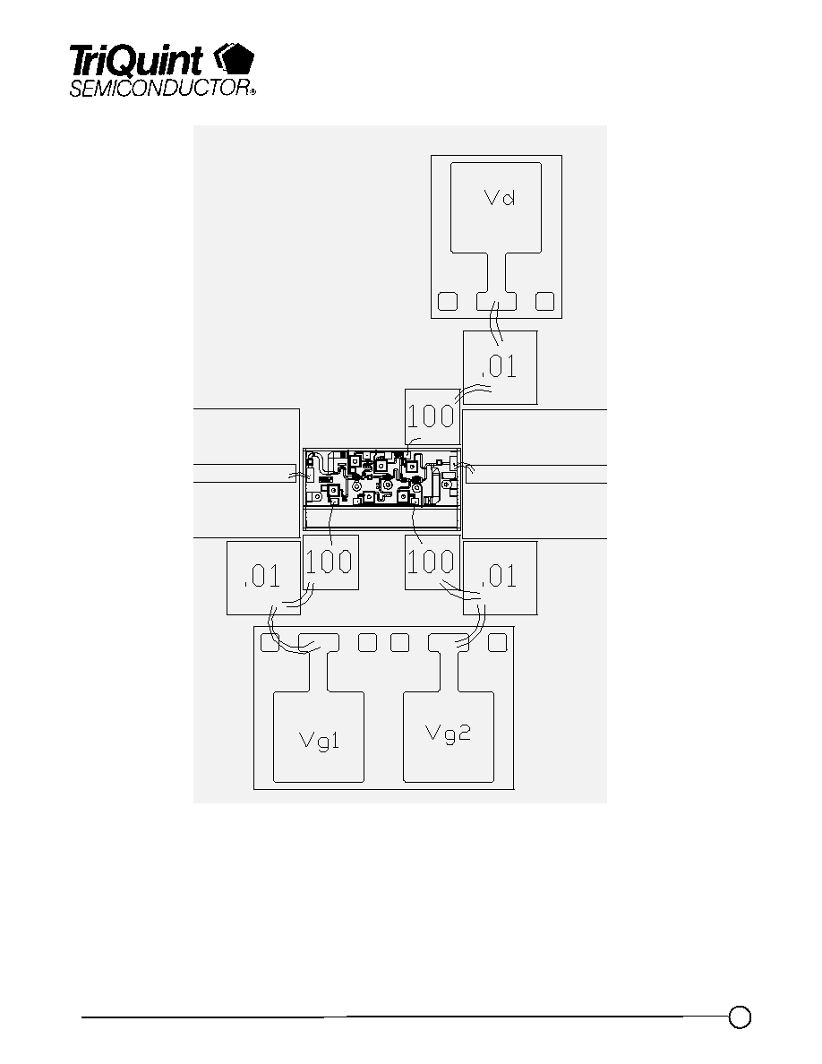
TGA1319C- Recommended Assembly Drawing
RFin
RFout
3
Notes:1. Vg1 and Vg2 may be sourced from the same supply.
2. Positive or negative gate bias may be required to
achieve recommended operating point.
TGA1319C-EPU
TriQuint Semiconductor Texas : Phone (972)994-8465 Fax (972)994 8504 Web: www.triquint.com
Advance Product Information
November 6, 2001
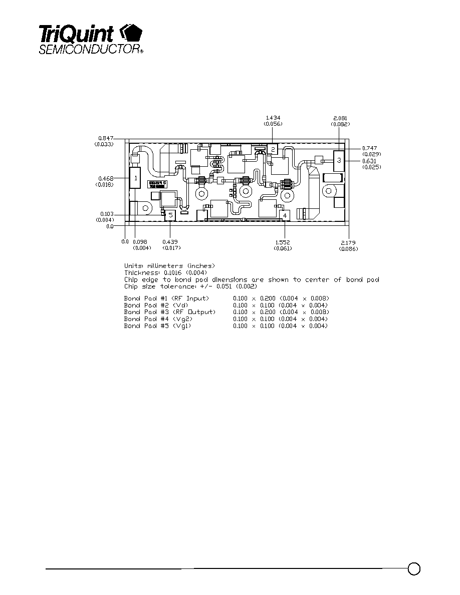
Mechanical Drawing
Note: Devices designated as EPU are typically early in their characterization process prior to finalizing all electrical and process
specifications. Specifications subject to change without notice
4
TGA1319C-EPU

TriQuint Semiconductor Texas : Phone (972)994-8465 Fax (972)994 8504 Web: www.triquint.com
Advance Product Information
November 6, 2001
Assembly Process Notes
GaAs MMIC devices are susceptible to damage from Electrostatic Discharge. Proper precautions should
be observed during handling, assembly and test.
Reflow process assembly notes:
À
Use AuSn (80/20) solder with limited exposure to temperatures at or above 300
C.
À
An alloy station or conveyor furnace with reducing atmosphere should be used.
À
No fluxes should be utilized.
À
Coefficient of thermal expansion matching is critical for long-term reliability.
À
Devices must be stored in a dry nitrogen atmosphere.
Component placement and adhesive attachment assembly notes:
À
Vacuum pencils and/or vacuum collets are the preferred method of pick up.
À
Air bridges must be avoided during placement.
À
The force impact is critical during auto placement.
À
Organic attachment can be used in low-power applications.
À
Curing should be done in a convection oven; proper exhaust is a safety concern.
À
Microwave or radiant curing should not be used because of differential heating.
À
Coefficient of thermal expansion matching is critical.
Interconnect process assembly notes:
À
Thermosonic ball bonding is the preferred interconnect technique.
À
Force, time, and ultrasonics are critical parameters.
À
Aluminum wire should not be used.
À
Discrete FET devices with small pad sizes should be bonded with 0.0007-inch wire.
À
Maximum stage temperature is 200
C.
8
TGA1319C-EPU