TriQuint Semiconductor Texas : Phone (972)994-8465 Fax (972)994 8504 Web: www.triquint.com
Product Data Sheet
1
Not Recommended for New Designs.
TriQuint Recommends the TGA2503-EPU be used for New Designs.
13.75 - 15 GHz 2 Watt Power Amplifier TGA1152-SCC
Key Features
Ę
0.5 um pHEMT Technology
Ę
34 dB Nominal Gain
Ę
33 dBm Nominal Pout @ Pin = 3 dBm
Ę
OTOI 39dBm Typical
Ę
Bias 7V @ 682 mA
Ę
Chip Dimensions 1.390mm x 2.495mm
Primary Applications
Ę
Ku Band Sat-Com
Ę
Point-to-Point Radio
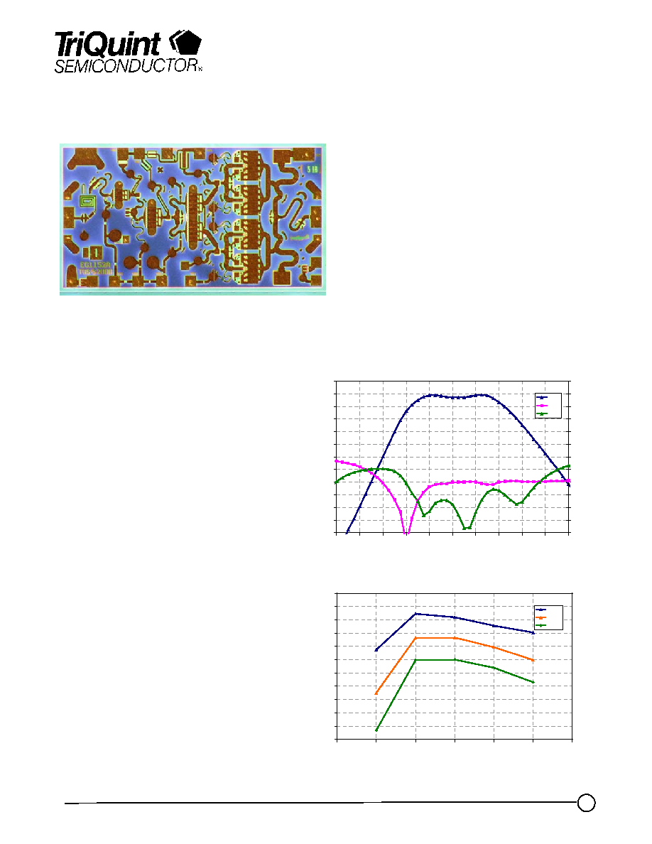
The TriQuint TGA1152-SCC MMIC is a
34dB gain, 2W, 13.75 Ł 15 GHz HPA,
which is ideally suited for current Ku-
Band satellite ground terminal
applications. Utilizing TriQuint's robust
0.5um power pHEMT process coupled
with the latest High Density Interconnect
(HDI) technology. The TGA1152-SCC
provides the high power transmit function
in an extremely compact (< 3.5mm
2
) chip
footprint.
The combination of a high-yield process,
electrical performance, and compact die
size is exactly what is required to support
the aggressive pricing targets required for
low-cost transmit modules. Each device
is 100% DC and RF tested on Łwafer to
ensure performance compliance. The
device is available in chip form.
March 19, 2001
S21
S11
S22
-20
-15
-10
-5
0
5
10
15
20
25
30
35
40
10
11
12
13
14
15
16
17
18
19
20
Frequency (GHz)
S
21 (dB)
-30
-25
-20
-15
-10
-5
0
5
10
15
20
25
30
S
11,
S
22 (dB)
S21
S11
S22
29
29.5
30
30.5
31
31.5
32
32.5
33
33.5
34
34.5
12.5
13
13.5
14
14.5
15
15.5
Frequency (GHz)
Pow
e
r (dBm
)
Psat
P2dB
P1dB
Product Description

TriQuint Semiconductor Texas : Phone (972)994-8465 Fax (972)994 8504 Web: www.triquint.com
Product Data Sheet
2
Not Recommended for New Designs.
TriQuint Recommends the TGA2503-EPU be used for New Designs.
MAXIMUM RATINGS
SYMBOL
PARAMETER 5/
VALUE
NOTES
V
+
POSITIVE SUPPLY VOLTAGE
8 V
4/
V
-
NEGATIVE SUPPLY VOLTAGE RANGE
-5V TO 0V
I
+
POSITIVE SUPPLY CURRENT (QUIESCENT)
1.023 A
4/
| I
G
|
GATE SUPPLY CURRENT
35.2 mA
P
IN
INPUT CONTINUOUS WAVE POWER
21.4 dBm
P
D
POWER DISSIPATION
9.404 W
3/ 4/
T
CH
OPERATING CHANNEL TEMPERATURE
150
0
C
1/ 2/
T
M
MOUNTING TEMPERATURE
(30 SECONDS)
320
0
C
T
STG
STORAGE TEMPERATURE
-65 to 150
0
C
1/
These ratings apply to each individual FET.
2/
Junction operating temperature will directly affect the device median time to failure (T
M
). For maximum life,
it is recommended that junction temperatures be maintained at the lowest possible levels.
3/
When operated at this bias condition with a base plate temperature of 70
0
C, the median life is reduced from
8.9E+6 to 4.2 E+4 hours.
4/
Combinations of supply voltage, supply current, input power, and output power shall not exceed P
D
.
5/
These ratings represent the maximum operable values for this device.
TGA1152-SCC
THERMAL INFORMATION*
Parameter
Test Conditions
T
CH
(
o
C)
R
qJC
(
░C/W)
T
M
(HRS)
R
qJC
Thermal Resistance
(channel to backside of
carrier)
Vd = 7V
I
D
= 682 mA
Pdiss = 4.774 W
125.74
11.67
8.9E+6
Note: Assumes eutectic attach using 1.5 mil 80/20 AuSn mounted to a 20 mil CuMo Carrier at
70
░C baseplate temperature. Worst case condition with no RF applied, 100% of DC power
is dissipated.
* The thermal information is a result of a detailed thermal model
.

TriQuint Semiconductor Texas : Phone (972)994-8465 Fax (972)994 8504 Web: www.triquint.com
Product Data Sheet
3
Not Recommended for New Designs.
TriQuint Recommends the TGA2503-EPU be used for New Designs.
DC SPECIFICATIONS (100%)
(T
A
= 25
░C + 5 ░C)
NOTES
SYMBOL
TEST CONDITIONS 2/
LIMITS
UNITS
MIN
MAX
I
DSS
STD
Info only
200
mA
Gm
STD
Info only
252
mS
1/
|V
P1
|
STD
0.5
1.5
V
1/
|V
P2
|
STD
0.5
1.5
V
1/
|V
P3
|
STD
0.5
1.5
V
1/
|V
BVGD1-3
|
STD
11
30
V
1/
|V
BVGD4
|
STD
11
30
V
1/
|V
BVGS
|
STD
11
30
V
1/
V
P
, V
BVGD
, and V
BVGS
are negative.
2/
The measurement conditions are subject to change at the manufacture's discretion
RF SPECIFICATIONS
(T
A
= 25
░C + 5░C)
TEST
MEASUREMENT
CONDITIONS
VALUE
UNITS
7V @ 682mA +/- 5%
MIN
TYP
MAX
SMALL-SIGNAL
GAIN MAGNITUDE
FREQ = 13.75 Ł 15 GHz
29
34
-
dB
POWER OUTPUT
at PIN= +3 dBm
FREQ = 13.75 Ł 14.5 GHz
31.5
33
-
dBm
INPUT RETURN LOSS
MAGNITUDE
FREQ = 13.75 Ł 15 GHz
-
-12
-
dB
OUTPUT RETURN LOSS
MAGNITUDE
FREQ = 13.75 Ł 15 GHz
-
-12
-
dB
GAIN FLATNESS
FREQ = 14 Ł 14.5 GHz
FREQ = 13.5 Ł 14.5 GHz
-
+/- 0.25
+/- 1.0
-
dB
dB
IMD3@SCL = P1dB Ł 10dB FREQ = 13.5 Ł 15 GHz
-
35
-
dBc
OIP3 (P1dB Ł 10dB)
FREQ = 13.5 Ł 15 GHz
-
39
-
dBc
TGA1152-SCC
TriQuint Semiconductor Texas : Phone (972)994-8465 Fax (972)994 8504 Web: www.triquint.com
Product Data Sheet
4
Not Recommended for New Designs.
TriQuint Recommends the TGA2503-EPU be used for New Designs.
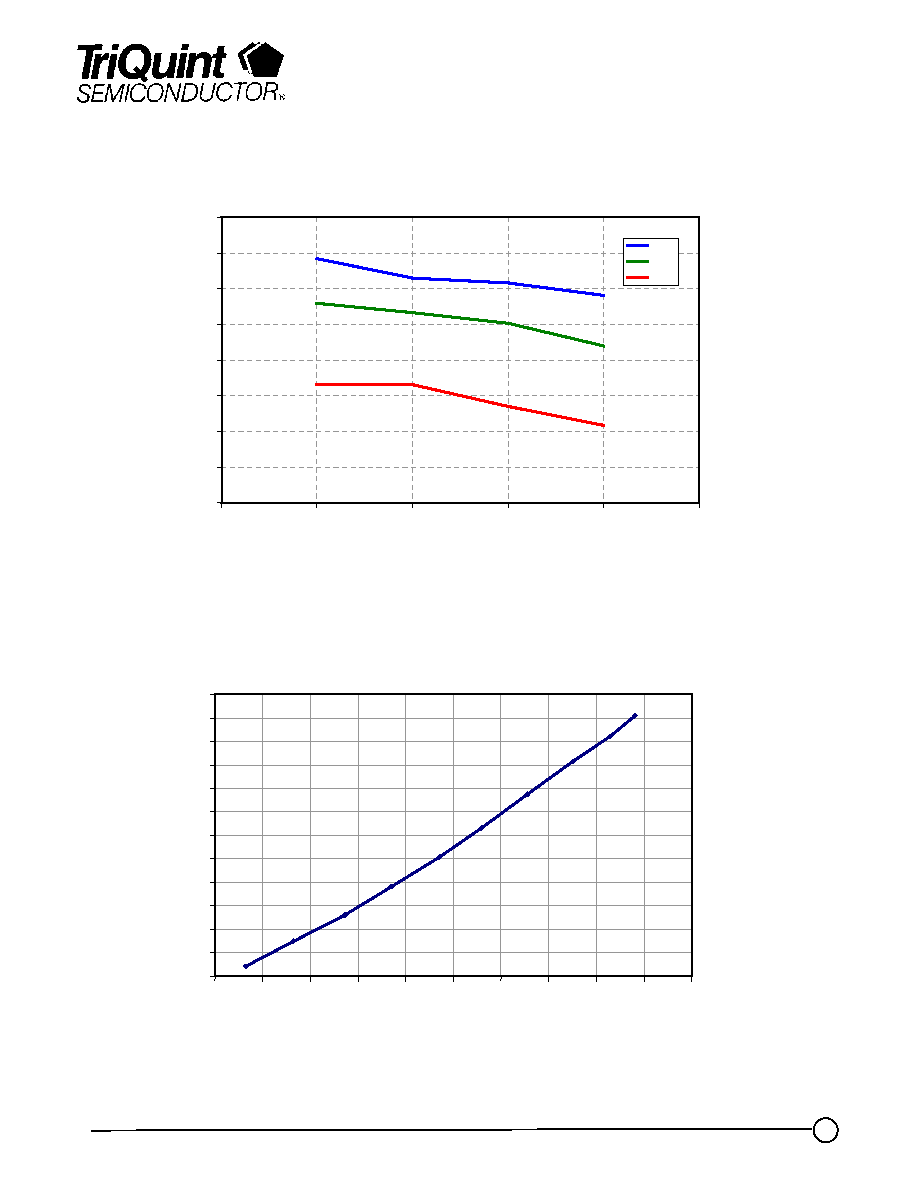
29.5
30
30.5
31
31.5
32
32.5
33
33.5
13
13.5
14
14.5
15
15.5
Frequency (GHz)
P
out@P
in=1dBm
-40C
25C
70C
TGA1152-SCC Over Temperature Measured Performance
6V @ 680mA
F=14GHz, Vd=7V/680mA, tone separation=10MHz
-45
-40
-35
-30
-25
-20
-15
-10
-5
0
5
10
15
10
12
14
16
18
20
22
24
26
28
30
Fundamental output power/tone (dBm)
M
e
a
n
IM
D
3
level (
d
Bm)
TGA1152-SCC IMD3 Performance
TGA1152-EPU
TriQuint Semiconductor Texas : Phone (972)994-8465 Fax (972)994 8504 Web: www.triquint.com
Product Data Sheet
5
Not Recommended for New Designs.
TriQuint Recommends the TGA2503-EPU be used for New Designs.
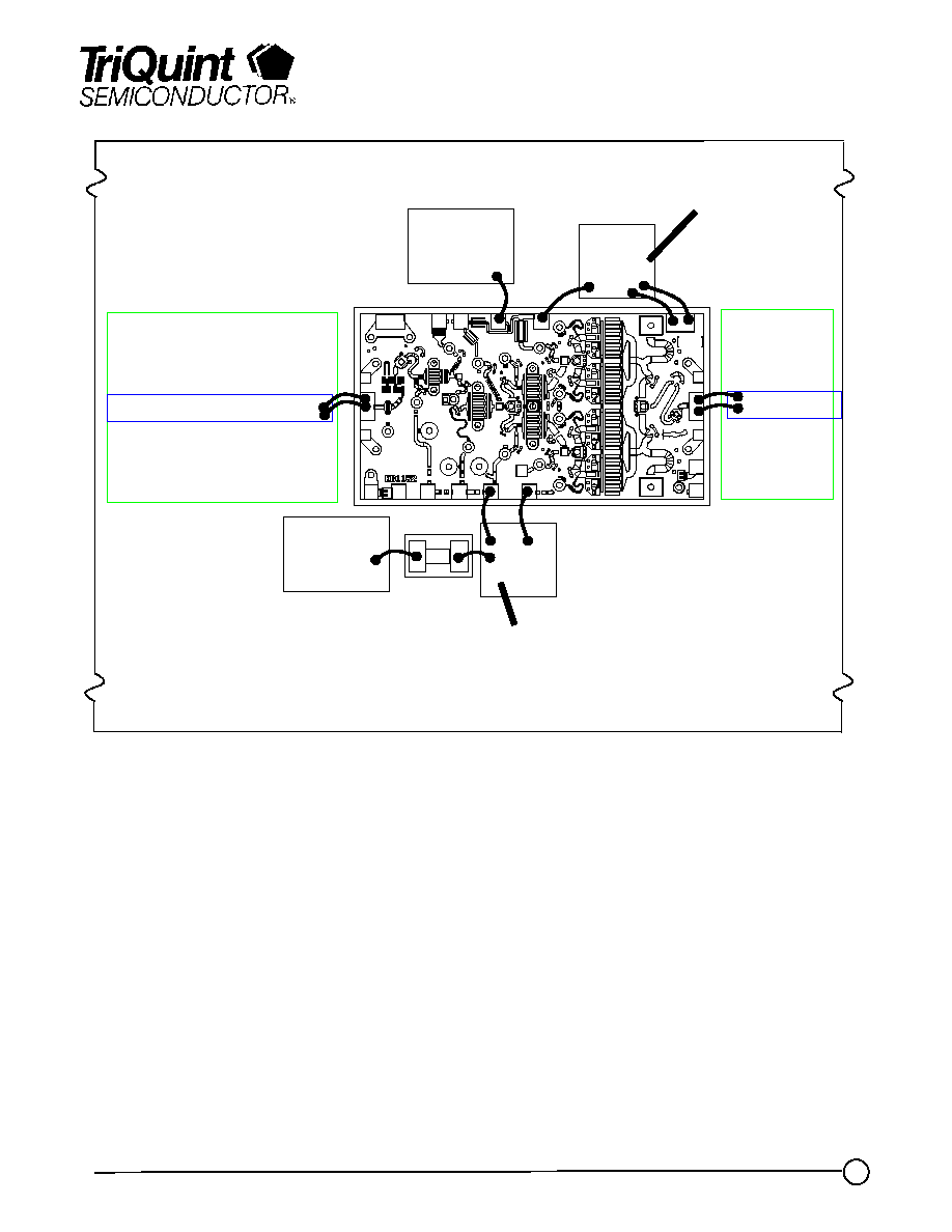
Output TFN
Vd = +7V
100pF
0.01
mF
Notes:
1. 0.1
mF capacitors on gate, drain
lines not shown but used
Input TFN
Cu-moly carrier plate (20mil thick)
100pF
Vg
0.01
mF
50
W
GaAs MMIC devices are susceptible to damage from Electrostatic Discharge. Proper precautions should
be observed during handling, assembly and test.
Recommended Assembly Diagram
TGA1152-SCC

TriQuint Semiconductor Texas : Phone (972)994-8465 Fax (972)994 8504 Web: www.triquint.com
Product Data Sheet
6
Not Recommended for New Designs.
TriQuint Recommends the TGA2503-EPU be used for New Designs.
TGA1152-SCC
TriQuint Semiconductor Texas : Phone (972)994-8465 Fax (972)994 8504 Web: www.triquint.com
Product Data Sheet
7
Not Recommended for New Designs.
TriQuint Recommends the TGA2503-EPU be used for New Designs.
GaAs MMIC devices are susceptible to damage from Electrostatic Discharge. Proper precautions should
be observed during handling, assembly and test.
TGA1152-SCC
Reflow process assembly notes:
Ę Use AuSn (80/20) solder with limited exposure to temperatures at or above 300¦C.
Ę An alloy station or conveyor furnace with reducing atmosphere should be used.
Ę No fluxes should be utilized.
Ę Coefficient of thermal expansion matching is critical for long-term reliability.
Ę Devices must be stored in a dry nitrogen atmosphere.
Component placement and adhesive attachment assembly notes:
Ę Vacuum pencils and/or vacuum collets are the preferred method of pick up.
Ę Air bridges must be avoided during placement.
Ę The force impact is critical during auto placement.
Ę Organic attachment can be used in low-power applications.
Ę Curing should be done in a convection oven; proper exhaust is a safety concern.
Ę Microwave or radiant curing should not be used because of differential heating.
Ę Coefficient of thermal expansion matching is critical.
Interconnect process assembly notes:
Ę Thermosonic ball bonding is the preferred interconnect technique.
Ę Force, time, and ultrasonics are critical parameters.
Ę Aluminum wire should not be used.
Ę Discrete FET devices with small pad sizes should be bonded with 0.0007-inch wire.
Ę Maximum stage temperature is 200¦C.