TPD1038F
2004-01-22
1
Toshiba Intelligent Power Device Silicon Monolithic Power MOS Integrated circuit
TPD1038F
Motor, Solenoid, Lamp Drivers
High Side Power Switch
TPD1038F is a monolithic power IC for high-side switches. The
IC has a vertical MOS FET output which can be directly driven
from a CMOS or TTL logic circuit (eg, an MPU). The device offers
intelligent self-protection and diagnostic functions.
Features
· A monolithic power IC with a structure combining a control
block (Bi-CMOS) and a vertical power MOS FET on a single
chip.
· One side of load can be grounded to a high-side switch.
· Can directly drive a power load from a microprocessor.
· Built-in protection against overheating and load short
circuiting.
· Incorporates a diagnosis function that allows diagnosis output to be read externally at load short-circuiting,
opening, or overheating.
· Up to -(50-V
DD
) -(60-V
DD
) of counterelectromotive force from an L load can be applied.
· Low on Resistance : R
DS(ON)
=120m(max) ( @ V
DD
= 12 VTa = 25Io = 2 A)
· 8-pin SOP package for surface mounting can be packed in tape.
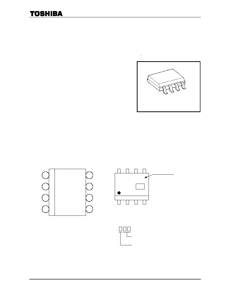
Pin Assignment Marking
That because of its MOS structure, this product is sensitive to static electrocity.
SOP8-P-1.27A
Weight0.08g(typ.)
IN
1
2
3
4
8
7
6
5
V
DD
OUT
GND
DIAG
V
DD
V
DD
V
DD
(TOP VIEW)
TPD1038
F
Product No.
() on lower left of the marking indicates Pin1.
Lot Number
Weekly code : (Three digits)
Week of manufacture
(01 for first of year, continues up to 52 or 53)
Year of manufacture
(One low-order digits of calendar year)

TPD1038F
2004-01-22
2
Block Diagram
Pin Description
Pin No.
Symbol
Function
1 OUT
Output pin. When the load is short circuited and current in excessof the detection current (3A min)
flows to the output pin , the output automatically turns on or off.
2 GND
Ground
pin.
3 DIAG
Self-diagnosis detection pin.Goes low when overheating is detected or when output is short circuit
with input on (high). N-channel open drain.
4 IN
Input pin. Input is CMOS compatible, with pull down resistor connected. Even if the input is open,
output will not accidentally turn on.
5,6,7,8 V
DD
Power
pin.
V
DD
OUT
5V regulator
Bandgap
MOSFET
(-MOS)
charge pump
driver
current detection
overheat detection
DIAG
GND
IN
TPD1038F
2004-01-22
3
Timing Chart
Truth Table
Input signal
Diagnosis
output
Output signal Output state
Operating state
H H H on
L L L off
Normal
H L L
current limit
(switching)
L L L off
Load Short
H L L off
L L L off
Overheating
H H H on
L H H off
Load open
H L L off
L H H off
Overheating and
load open
Input signal
Overcurrent detection
Load open
Output current
Channel temperature
Overheating detection 150(min)
Hy
st
e
r
e
s
i
s
5
(t
y
p
.
)
T
ch
Diagnostic output
Current limit
Thermal shutdown
Load open detection
Normal
Output signal

TPD1038F
2004-01-22
4
Maximum Ratings (Ta = 25°C)
Characteristics Symbol Rating
Unit
Drain-Source Voltage
V
DS
60 V
DC
V
DD(1)
25 V
Supply Voltage
Pulse
V
DD(2)
60(R
S
=1,=250ms)
V
DC
V
IN(1)
0.512 V
Input Voltage
Pulse
V
IN(2)
V
DD(1)
+1.5(t=100ms) V
Diagnosis Output Voltage
V
DIAG
0.525 V
Output Current
I
O
Internally
Limited
A
Input current
I
IN
±
10 mA
Diagnosis current
I
DIAG
5
mA
Power Dissipation
(Note 1-a)
P
D(1)
1.1 W
Power Dissipation
(Note 1-b)
P
D(2)
0.425 W
Operating temperature
Topr
40110 °C
Channel temperature
T
ch
150
°C
Storage temperature
T
stg
55150 °C
Thermal Resistance
Characteristic Symbol
Rating
Unit
113.5 (Note1-a)
Thermal Resistance
R
th(ch-a)
294.0 (Note1-b)
°C /W
Note 1:
1-a : Mounted on glass epoxy board (a) 1-b : Mounted on glass epoxy board (b)
FR-4
25.4×25.4×0.8
(Unitmm)
FR-4
25.4×25.4×0.8
(Unitmm)

TPD1038F
2004-01-22
5
Electrical characteristics (T
a
=25°C)
Characteristics Symbol
Test
circuit
Test condition
min
typ.
max
Unit
Operating supply voltage
V
DD(OPR)
6 12 18 V
Current dissipation
I
DD
V
DD
=12V, V
IN
=0V, R
L
=10
3 mA
H-level input voltage
V
IH
V
DD
=12V
3.5
V
L-level input voltage
V
IL
V
DD
=12V
1.5 V
H-level input current
I
IH
V
DD
=12V, V
IN
=5V
200
A
On resistance
R
DS(ON)
V
DD
=12V, I
O
=2A
0.12
Output leakage current
I
OL
V
DD
=12V
1 mA
Diagnosis
output voltage
"L"-level
V
DL
V
DD
=12V, V
IN
=0V, I
DL
=1mA
R
L
=10
0.4
V
Diagnosis
output current
"H"-level
I
DH
V
DD
=12V, V
IN
=5V, R
L
=10,
V
DH
=12V
10
A
I
OC(1)
(Note2)
12
V
DD
=12V
3
9 A
Over current detection
I
OC(2)
(Note3)
3
V
DD
=12V, R
L
=0.1
10 A
Overheating detection
T
OT
V
DD
=12V
150
200
Load open detection (Note4)
R
op
V
DD
=12V, V
IN
=0V
5 17
k
t
on
100
s
Switching time
t
off
4
V
DD
=12V, R
L
=10
40
s
t
DLH
70
s
Diagnosis delay time
t
DHL
5
V
DD
=12V, R
L
=10
22
s
Output clamp voltage
V
clamp
V
DD
=12V, V
IN
=0V, I
O
=1A, L=10mH
-
(60-
V
DD
)
-
(50-
V
DD
)
(Note 2) Over current detection
(Note 3) Peak current @ current limit function
(Note 4) Load open detection function :
V
DD
= 8 18V
Test circuit 1
Over current detection I
OC(1)
Over current detection when load current is increased while VIN = "H"
V
DIAG
I
O
I
OC(1)
5V
0V
0.4V
V
DL
0
TPD1038F
V
DD
=12V
OUT
R
L
I
O
5V
2.5k
V
DIAG
V
IN
5V
DIAG

TPD1038F
2004-01-22
6
Test circuit 2
Over current detection I
OC(1)
Over current detection when load is short circuit and VIN = "L" "H"
Test circuit 3
Over current detection I
OC(2)
Test circuit 4
Switching time t
on
, t
off
Test circuit 5
Diagnosis delay time t
DLH
, t
DHL
V
IN
I
O
I
OC(2)
TPD1038F
V
DD
=12V
OUT
R
L
I
O
5V
2.5k
V
DIAG
V
IN
P.G
DIAG
V
DIAG
I
O
I
OC(1)
5V
0V
0.4V
V
DL
0
TPD1038F
V
DD
=12V
OUT
R
L
=0.1
I
O
5V
2.5k
V
DIAG
V
IN
P.G
DIAG
TPD1038F
V
DD
=12V
OUT
R
L
=10
V
IN
P.G
DIAG
V
OUT
V
OUT
V
IN
90%
90%
10%
10%
t
on
t
off
5V
12V
90%
10%
0.1s
0.1s
R
L
=10
TPD1038F
V
DD
=12V
OUT
V
IN
P.G
V
DIAG
5V
5k
V
DIAG
V
IN
50%
90%
10%
50%
t
DLH
t
DHL
5V
5V
90%
10%
0.1s
0.1s
0V
TPD1038F
2004-01-22
7
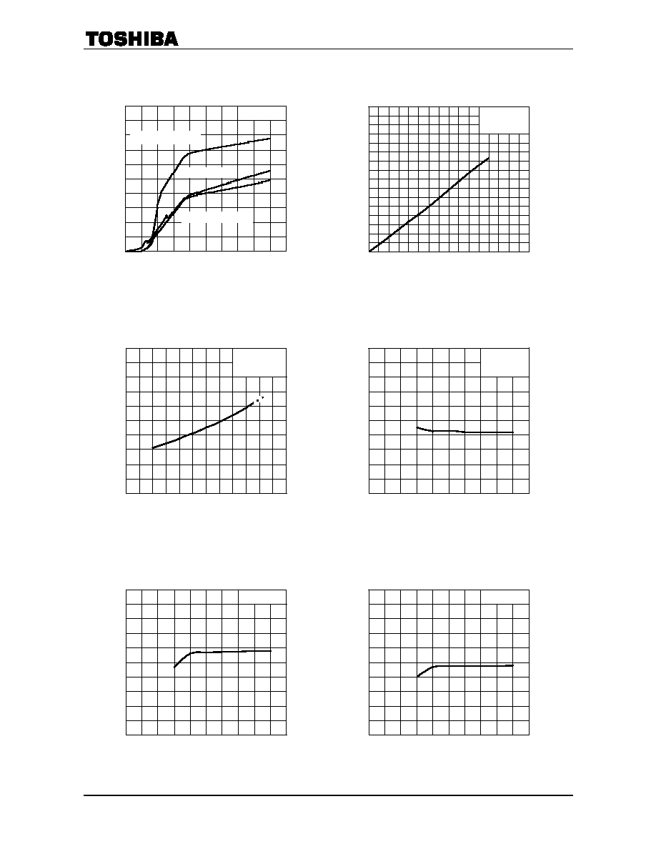
V
IL
- V
DD
0
1
2
3
4
5
0
4
8
12
16
20
SUPPLY VOLTAGE V
DD
(V)
L-
L
E
V
EL
I
N
PU
T
V
O
L
T
A
G
E
V
IL
(V
)
Tch=25°C
V
IH
- V
DD
0
1
2
3
4
5
0
4
8
12
16
20
SUPPLY VOLTAGE V
DD
(V)
H
-
LE
V
E
L I
N
P
U
T
V
O
LT
A
G
E
V
IH
(V
)
Tch=25°C
R
DS(ON)
- V
DD
0
0.04
0.08
0.12
0.16
0.2
0
4
8
12
16
20
SUPPLY VOLTAGE V
DD
(V)
O
N
R
E
SI
ST
A
N
C
E
R
DS
(
O
N
)
(
)
IO=2A
Tch=25°C
R
DS(ON)
- T
ch
0
0.04
0.08
0.12
0.16
0.2
-80
-40
0
40
80
120
160
OPERATING TEMPERATURE T
ch
(°C)
O
N
RE
S
I
S
T
A
NCE
R
DS
(
O
N)
(
)
VDD=12V
IO=2A
V
DS(ON)
- I
O
0
0.05
0.1
0.15
0.2
0.25
0.3
0.35
0.4
0
0.5
1
1.5
2
2.5
3
3.5
4
OUTPUT CURRENT I
O
(A)
O
N
VO
L
T
AG
E
V
DS
(O
N)
(V
)
VDD=12V
Tch=25°C
I
DD
- V
DD
0
0.5
1
1.5
2
2.5
0
4
8
12
16
20
SUPPLY VOLTAGE V
DD
(V)
CU
RRE
NT
DIS
S
I
P
A
T
I
O
N
I
DD
(m
A
)
RL=10VIN=0V
LOAD OPENVIN=5V
LOAD OPENVIN=0V
Tch=25°C
I
DD
V
DD
C
U
RRE
NT
DI
S
S
IP
A
T
IO
N
I
DD
(
m
A
)
V
DS(ON)
I
O
ON
VOL
T
AGE
V
DS
(
O
N
)
(
V
)
O
N
R
E
S
I
ST
AN
C
E
R
DS
(
O
N
)
(
)
R
DS(ON)
T
ch
R
DS(ON)
V
DD
O
N
R
E
S
I
ST
AN
C
E
R
DS
(
O
N
)
(
)
H
-
L
EVE
L
I
N
P
U
T
VOL
T
A
G
E
V
IH
(V
)
V
IH
V
DD
V
IL
V
DD
L
-
LEVEL
I
N
P
U
T
VOL
T
AG
E V
IL
(V
)
CHANNEL TEMPERATURE T
ch
(°C)
SUPPLY VOLTAGE V
DD
(V)
SUPPLY VOLTAGE V
DD
(V)
SUPPLY VOLTAGE V
DD
(V)
SUPPLY VOLTAGE V
DD
(V)
OUTPUT CURRENT I
O
(A)

TPD1038F
2004-01-22
8
t
DHL
- T
ch
0
10
20
30
40
-80
-40
0
40
80
120
160
OPERATING TEMPERATURE T
ch
(°C)
DI
A
G
N
O
S
I
S
DE
L
A
Y
T
I
ME
t
DHL
(µ
s
)
VDD=6V
VDD=18V
VDD=12V
RL=10
t
DLH
T
ch
0
40
80
120
160
200
-80
-40
0
40
80
120
160
OPERATING TEMPERATURE T
ch
(°C)
VDD=6V
VDD=18V
VDD=12V
RL=10
SWITCHING CHARACTERISTICS
0
40
80
120
160
0
4
8
12
16
20
SUPPLY VOLTAGE V
DD
(V)
SW
I
T
C
H
I
N
G
T
I
M
E
(µ
s
)
tON
tOFF
RL=10
Tch=25°C
I
OC
- T
ch
0
2
4
6
8
10
12
-80
-40
0
40
80
120
160
OPERATING TEMPERATURE T
ch
(°C)
O
V
E
R
CURRE
NT
P
R
O
T
E
C
T
I
O
N
I
OC
(A
)
IOC(2)
IOC(1)
VDD=12V
V
clamp
- T
ch
-80
-60
-40
-20
0
-80
-40
0
40
80
120
160
OPERATING TEMPERATURE T
ch
(°C)
VDD=12V
VIN=0V
IO=1A
L=10mH
V
DL
- T
ch
0
40
80
120
160
200
-80
-40
0
40
80
120
160
OPERATING TEMPERATURE T
ch
(°C)
IDL=1mA
IDL=2mA
VDD=12V
O
V
E
R
CU
RRE
NT DE
T
E
CT
I
O
N
I
OC
(A)
I
OC
T
ch
V
DL
T
ch
DI
A
G
NO
S
I
S
O
U
T
P
UT
V
O
L
T
A
G
E
V
DL
(m
V)
V
clamp
T
ch
O
U
T
P
UT
CL
A
M
P
V
O
L
T
A
G
E
V
cl
a
m
p
(V)
S
W
I
T
CHI
NG
T
I
ME
(
µ
s)
SWITCHING CHARACTERISTICS
D
I
AG
N
O
SI
S D
E
L
A
Y
T
I
M
E
t
DL
H
(
µ
s)
t
DLH
T
ch
t
DHL
T
ch
D
I
AG
N
O
SI
S D
E
L
A
Y
T
I
M
E
t
DHL
(
µ
s)
SUPPLY VOLTAGE V
DD
(V)
CHANNEL TEMPERATURE T
ch
(°C)
CHANNEL TEMPERATURE T
ch
(°C)
CHANNEL TEMPERATURE T
ch
(°C)
CHANNEL TEMPERATURE T
ch
(°C)
CHANNEL TEMPERATURE T
ch
(°C)

TPD1038F
2004-01-22
9
R
OP
- T
ch
0
10
20
30
40
50
-80
-40
0
40
80
120
160
OPERATING TEMPERATURE T
ch
(°C)
L
O
A
D
O
P
E
N
DE
T
E
CT
I
O
N R
OP
(k
)
ROPL
ROPH
VDD=12V
ROPH:LOAD OPEN DETECTION RESITANCE
ROPL:LOAD OPEN DETECTION RESET RESISTANCE
R
OP
- V
DD
0
20
40
60
80
100
0
4
8
12
16
20
SUPPLY VOLTAGE V
DD
(V)
L
O
A
D
O
P
E
N
DE
TE
CTI
O
N
R
OP
(
k
)
ROPL
ROPH
Tch=25°C
ROPH:LOAD OPEN DETECTION RESITANCE
ROPL:LOAD OPEN DETECTION RESET RESISTANCE
P
D
- T
a
0
0.4
0.8
1.2
1.6
-40
0
40
80
120
160
AMBIENT TEMPERATURE Ta
(°C)
P
O
W
E
R DIS
S
I
P
A
T
I
O
N
P
D
(W
)
(2)
(1)
(1)MOUNTED ON GLASS
EPOXY BOARD (a)
(2)MOUNTED ON GLASS
EPOXY BOARD(b)
V
DD
0
40
80
120
160
0
4
8
12
16
20
SUPPLY VOLTAGE V
DD
(V)
DIA
G
NO
S
I
S
DE
L
A
Y
T
I
M
E
(µ
s
)
tDLH
tDHL
Tch=25°C
RL=10
VDD
(V)
R
op
(k
t
DLH
,t
DHL
V
DD
DI
A
G
NO
S
I
S
DE
L
A
Y
T
I
M
E
t
DL
H
,t
DHL
(
µ
s)
L
O
A
D
O
P
E
N
DE
TE
CT
I
O
N
R
OP
(
k
)
R
OP
V
DD
R
OP
T
ch
L
O
A
D
O
P
E
N
DE
T
E
C
T
I
O
N
R
OP
(
k
)
P
D
Ta
P
O
WE
R DI
S
S
IP
A
T
I
O
N
P
D
(
W
)
AMBIENT TEMPERATURE Ta (°C)
CHANNEL TEMPERATURE T
ch
(°C)
SUPPLY VOLTAGE V
DD
(V)
SUPPLY VOLTAGE V
DD
(V)
r
th(ch-a)
- t
W
0.1
1
10
100
1000
0.001
0.01
0.1
1
10
100
1000
PULSE WIDTH t
w
(s)
T
R
A
N
SI
E
N
T
T
H
E
R
M
A
L
R
E
SI
ST
A
N
C
E
r
t
h
(
c
h-
a)
(°
C
/
W
)
(1)
(2)
(1)MOUNTED ON GLASS EPOXY BOARD(a)
(2)MOUNTED ON GLASS EPOXY BOARD(b)
SINGLE PULSE,Ta=25
TPD1038F
2004-01-22
10
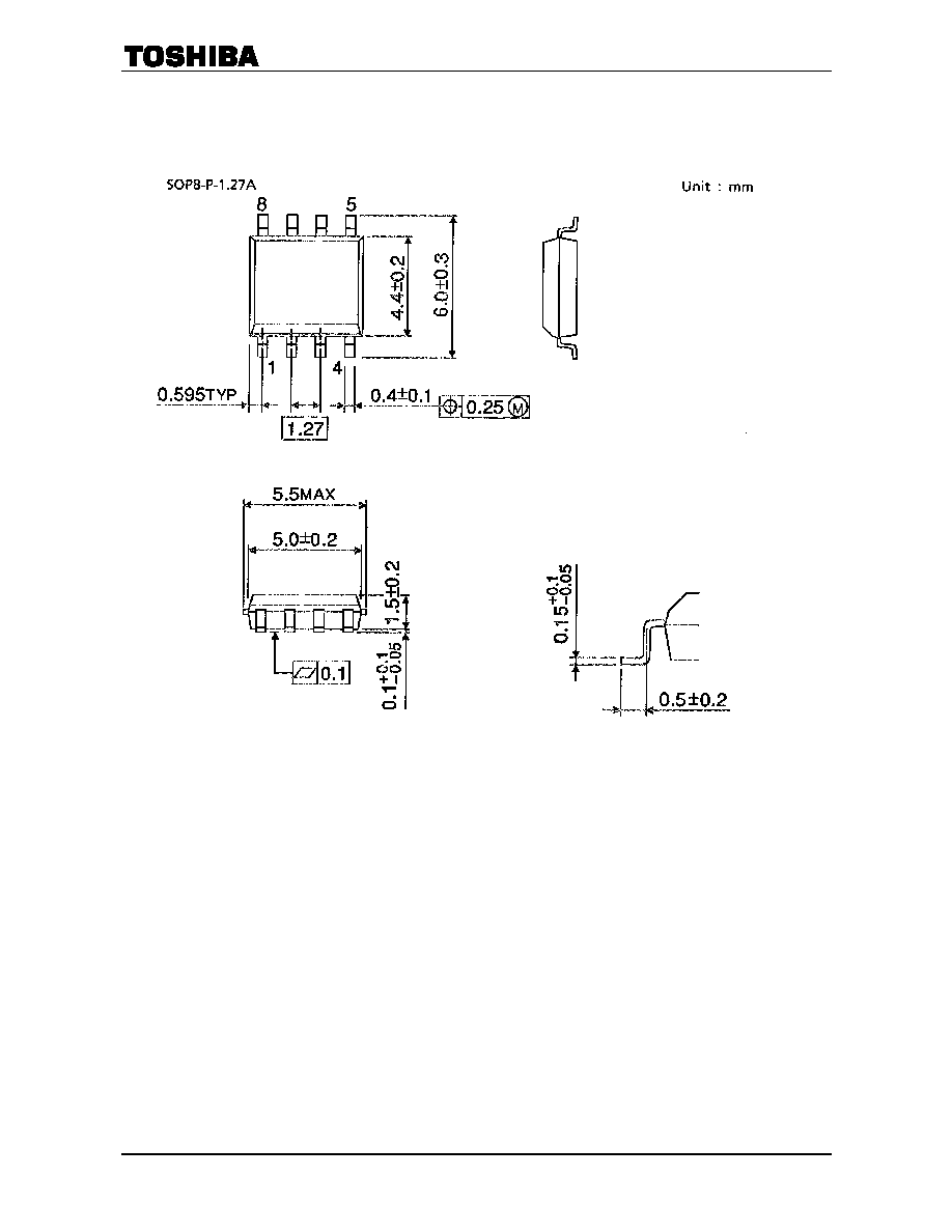
Package dimensions
Weight : 0.08g (typ.)

TPD1038F
2004-01-22
11
· The information contained herein is subject to change without notice.
· The information contained herein is presented only as a guide for the applications of our products. No
responsibility is assumed by TOSHIBA for any infringements of patents or other rights of the third parties which
may result from its use. No license is granted by implication or otherwise under any patent or patent rights of
TOSHIBA or others.
· TOSHIBA is continually working to improve the quality and reliability of its products. Nevertheless, semiconductor
devices in general can malfunction or fail due to their inherent electrical sensitivity and vulnerability to physical
stress. It is the responsibility of the buyer, when utilizing TOSHIBA products, to comply with the standards of
safety in making a safe design for the entire system, and to avoid situations in which a malfunction or failure of
such TOSHIBA products could cause loss of human life, bodily injury or damage to property.
In developing your designs, please ensure that TOSHIBA products are used within specified operating ranges as
set forth in the most recent TOSHIBA products specifications. Also, please keep in mind the precautions and
conditions set forth in the "Handling Guide for Semiconductor Devices," or "TOSHIBA Semiconductor Reliability
Handbook" etc..
· The TOSHIBA products listed in this document are intended for usage in general electronics applications
(computer, personal equipment, office equipment, measuring equipment, industrial robotics, domestic appliances,
etc.). These TOSHIBA products are neither intended nor warranted for usage in equipment that requires
extraordinarily high quality and/or reliability or a malfunction or failure of which may cause loss of human life or
bodily injury ("Unintended Usage"). Unintended Usage include atomic energy control instruments, airplane or
spaceship instruments, transportation instruments, traffic signal instruments, combustion control instruments,
medical instruments, all types of safety devices, etc.. Unintended Usage of TOSHIBA products listed in this
document shall be made at the customer's own risk.
· The products described in this document are subject to the foreign exchange and foreign trade laws.
030619EBA
RESTRICTIONS ON PRODUCT USE