TPD1028BS
2002-10-24
1
TOSHIBA Intelligent Power Device Silicon Monolithic Power MOS IC
TPD1028BS
Low-Side Switch for Motors, Solenoids, and Lamp Drivers
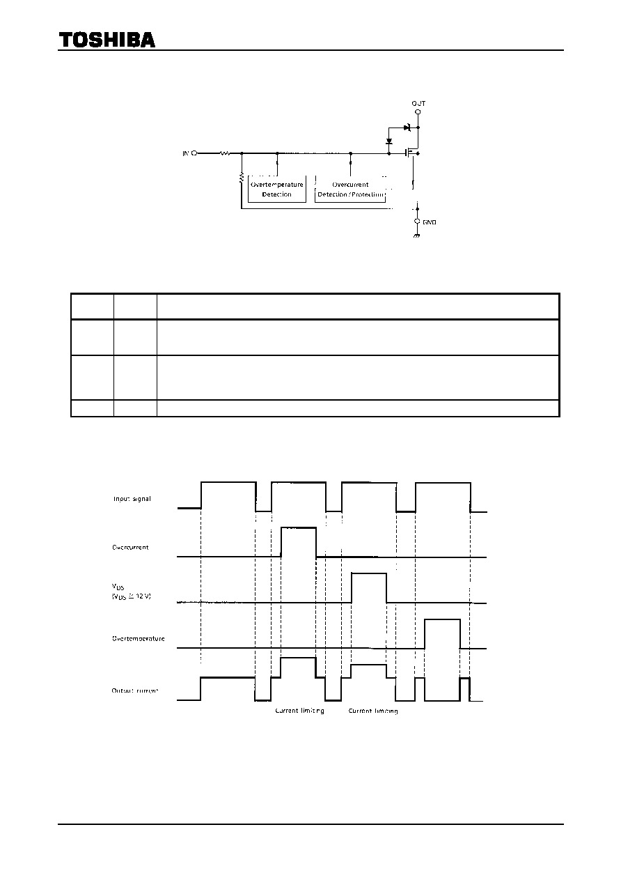
TPD1028BS is a monolithic power IC for low-side switch. The IC
has a vertical MOSFET output which can be directly driven from
a CMOS or TTL logic circuit (e.g., an MPU). The IC offers
intelligent self-protection functions.
Features
l A monolithic power IC with a new structure combining a
control block and a vertical power MOSFET (-MOS) on a
single chip.
l Can directly drive a power load from a CMOS or TTL logic.
l Built-in Protection circuits against overvoltage, load short
circuiting, and thermal shutdown.
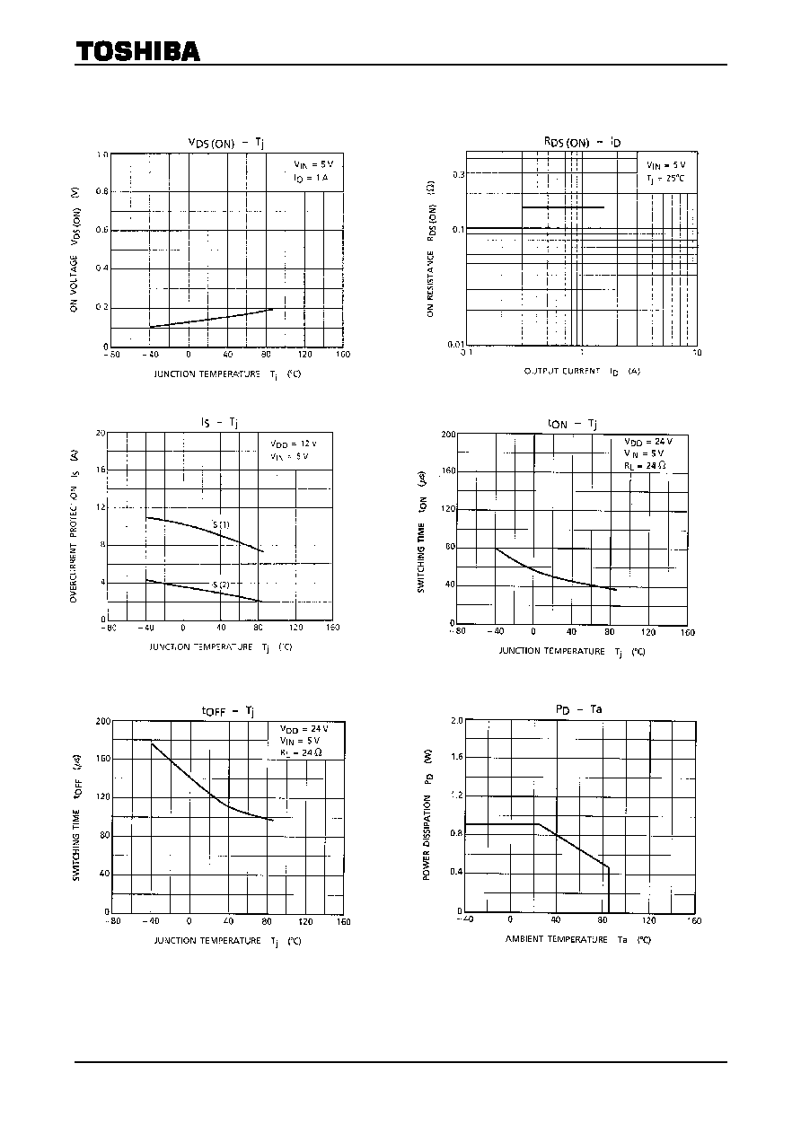
l Low on-resistance. R
DS (ON)
= 0.25 (max) (@V
IN
= 5 V, T
j
=
25°C)
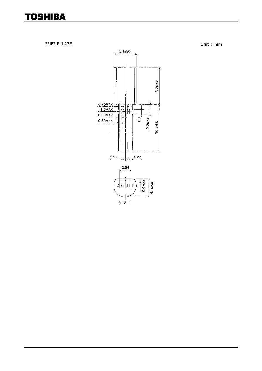
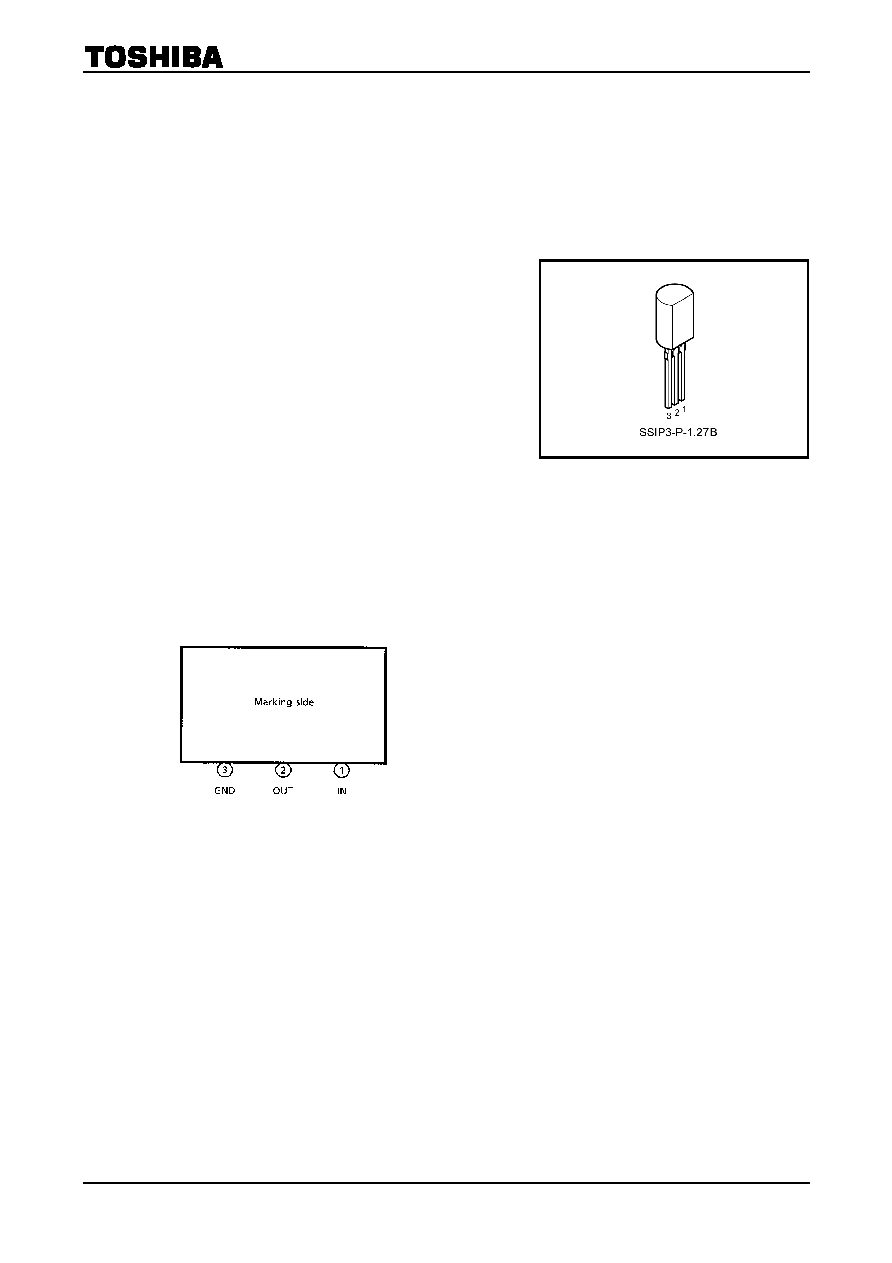
l Package TO-92(MOD) can be packed in tape.
Pin Assignment
Note:
That because of its MOS structure, this product is sensitive to static electricity.
Weight: 0.36 g (typ.)
TPD1028BS
2002-10-24
2
Block Diagram
Pin Description
Pin No.
Symbol
Pin Description
1 IN
Input pin.
This pin is connected to a pull-down resistor internally, so that even when input wiring is open-circuited,
outputcan never be turned on inadvertently.
2 OUT
Output pin.
If an inrush current flows (e.g., from a lamp), the current is clamped at 10 A (typ.) by an overcurrent
protective circuit. Also, a 150 µs (typ.) mask circuit is included internally, so that if V
DS
12 V (typ.) after this
mask time, the current is clamped at 3 A (typ.).
3 GND
Ground
pin.
Timing Chart
TPD1028BS
2002-10-24
4
Electrical Characteristics
(T
j
= 25°C)
Characteristic Symbol
Test
Cir-
cuit
Test Condition
Min
Typ.
Max
Unit
Drain-source breakdown
voltage
V
(BR) DSS
V
IN
= 0 V, I
D
= 10 mA
40
V
Operating supply voltage
V
DD
38 V
V
IH(1)
V
DS
= 24 V, I
D
= 1 A
4.5
5
5.5
V
IH(2)
V
DS
= 10 V, I
D
= 0.75 A
3.9
5
5.7
High level input voltage
V
IH(3)
V
DS
= 38 V, I
D
= 0.75 A
3.9
5
5.7
V
V
IL(1)
V
DS
= 24 V, I
D
= 10 µA
0.8
V
IL(2)
V
DS
= 10 V, I
D
= 10 µA
0.8
Low level input voltage
V
IL(3)
V
DS
= 38 V, I
D
= 10 µA
0.8
V
I
DSS(1)
V
IN
= 0 V, V
DS
= 40 V
100
Current at output off
I
DSS(2)
V
IN
= 0 V, V
DS
= 24 V
10
µA
Input current
I
IN
V
IN
= 5 V,
at normal operation
300
µA
On resistance
R
DS(ON)
V
IN
= 5 V, I
D
= 1 A
0.25
Thermal shutdown temperature
T
S
V
IN
= 5 V
160 °C
I
S(1)
V
DS
= 24 V, V
IN
= 5 V,
during inrush
10
Overcurrent protection
I
S(2)
V
DS
= 24 V, V
IN
= 5 V,
when shorted load
3
A
Shorted load detection
voltage
V
DS
when shorted load
12 V
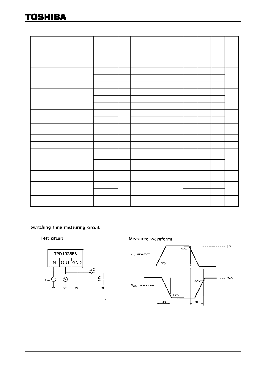
t
ON
70
Switching time
t
OFF
1
V
DS
= 24 V, V
IN
= 5 V,
R
L
= 24
120
µs
Diode forward voltage
between drain and source
V
DSF
I
F
= 1.5 A
0.9 1.8 V
Test Circuit 1

TPD1028BS
2002-10-24
8
· TOSHIBA is continually working to improve the quality and reliability of its products. Nevertheless, semiconductor
devices in general can malfunction or fail due to their inherent electrical sensitivity and vulnerability to physical
stress. It is the responsibility of the buyer, when utilizing TOSHIBA products, to comply with the standards of
safety in making a safe design for the entire system, and to avoid situations in which a malfunction or failure of
such TOSHIBA products could cause loss of human life, bodily injury or damage to property.
In developing your designs, please ensure that TOSHIBA products are used within specified operating ranges as
set forth in the most recent TOSHIBA products specifications. Also, please keep in mind the precautions and
conditions set forth in the "Handling Guide for Semiconductor Devices," or "TOSHIBA Semiconductor Reliability
Handbook" etc..
· The TOSHIBA products listed in this document are intended for usage in general electronics applications
(computer, personal equipment, office equipment, measuring equipment, industrial robotics, domestic appliances,
etc.). These TOSHIBA products are neither intended nor warranted for usage in equipment that requires
extraordinarily high quality and/or reliability or a malfunction or failure of which may cause loss of human life or
bodily injury ("Unintended Usage"). Unintended Usage include atomic energy control instruments, airplane or
spaceship instruments, transportation instruments, traffic signal instruments, combustion control instruments,
medical instruments, all types of safety devices, etc.. Unintended Usage of TOSHIBA products listed in this
document shall be made at the customer's own risk.
· The products described in this document are subject to the foreign exchange and foreign trade laws.
· The information contained herein is presented only as a guide for the applications of our products. No
responsibility is assumed by TOSHIBA CORPORATION for any infringements of intellectual property or other
rights of the third parties which may result from its use. No license is granted by implication or otherwise under
any intellectual property or other rights of TOSHIBA CORPORATION or others.
· The information contained herein is subject to change without notice.
000707EBA
RESTRICTIONS ON PRODUCT USE