
TPC8104-H
2002-09-11
1
TOSHIBA Field Effect Transistor Silicon P Channel MOS Type (High Speed U-MOSII)
TPC8104-H
High Speed and High Efficiency DC-DC Converters
Lithium Ion Battery Applications
Notebook PCs
Portable Equipment Applications
l Small footprint due to small and thin package
l High speed switching
l Small gate charge
: Qg = 17 nC (typ.)
l Low drain-source ON resistance : R
DS
(ON)
= 38 m (typ.)
l High forward transfer admittance : |Y
fs
| = 7.0 S (typ.)
l Low leakage current : I
DSS
= -10 µA (max) (V
DS
= -30 V)
l Enhancement-mode : V
th
= -0.8~-2.0 V (V
DS
= -10 V, I
D
= -1 mA)
Maximum Ratings
(Ta = 25°C)
Characteristics Symbol
Rating
Unit
Drain-source voltage
V
DSS
-30 V
Drain-gate voltage (R
GS
= 20 k)
V
DGR
-30 V
Gate-source voltage
V
GSS
±20 V
DC (Note
1)
I
D
-5
Drain current
Pulse (Note
1)
I
DP
-20
A
Drain power dissipation
(t = 10 s)
(Note
2a)
P
D
2.4
W
Drain power dissipation
(t = 10 s)
(Note
2b)
P
D
1.0
W
Single pulse avalanche energy
(Note
3)
E
AS
32.5
mJ
Avalanche current
I
AR
-5 A
Repetitive avalanche energy
(Note 2a) (Note 4)
E
AR
0.24
mJ
Channel temperature
T
ch
150
°C
Storage temperature range
T
stg
-55 to 150
°C
Note: For (Note 1), (Note 2), (Note 3) and (Note 4), please refer to the
next page.
This transistor is an electrostatic sensitive device. Please handle with
caution.
Unit: mm
JEDEC
JEITA
TOSHIBA 2-6J1B
Weight: 0.080 g (typ.)
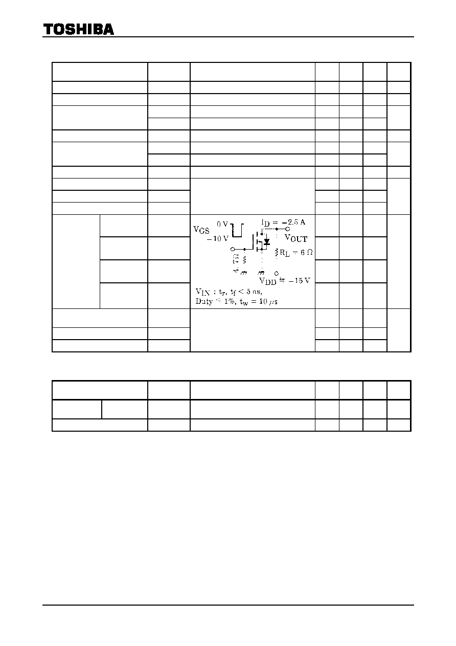
Circuit Configuration

TPC8104-H
2002-09-11
2
Thermal Characteristics
Characteristics Symbol
Max
Unit
Thermal resistance, channel to ambient
(t = 10 s)
(Note 2a)
R
th (ch-a)
52.1
°C/W
Thermal resistance, channel to ambient
(t = 10 s)
(Note 2b)
R
th (ch-a)
125
°C/W
Marking
(Note 5)
Note 1: Please use devices on condition that the channel temperature is below 150°C.
Note 2:
(a) Device mounted on a glass-epoxy board (a)
(b) Device mounted on a glass-epoxy board (b)
Note 3: V
DD
= -24 V, T
ch
= 25°C (initial), L = 1.0 mH, R
G
= 25 , I
AR
= -5 A
Note 4: Reptitve rating; pulse width limited by maximum channel temperature.
Note 5: on lower left of the marking indicates Pin 1.
shows Lot number. (year of manufacture: last decimal digit of the year of manufacture, month of
manufacture: january to december are denoted by letters A to L respectively)
Type
TPC8104
H
(a)
FR-4
25.4 × 25.4 × 0.8
(Unit:
mm)
(b)
FR-4
25.4 × 25.4 × 0.8
(Unit:
mm)
TPC8104-H
2002-09-11
3
Electrical Characteristics
(Ta = 25°C)
Characteristics Symbol
Test
Condition
Min
Typ.
Max
Unit
Gate leakage current
I
GSS
V
GS
= ±16 V
, V
DS
= 0 V
-- -- ±10
µA
Drain cut-off current
I
DSS
V
DS
= -30 V
, V
GS
= 0 V
-- -- -10
µA
V
(BR) DSS
I
D
= -10 mA
, V
GS
= 0 V
-30 -- --
Drain-source breakdown voltage
V
(BR) DSX
I
D
= -10 mA
, V
GS
= 20 V
-15 -- --
V
Gate threshold voltage
V
th
V
DS
= -10 V,
I
D
= -1 mA
-0.8 -- -2.0
V
R
DS (ON)
V
GS
= -4 V,
I
D
= -2.5 A
-- 68 120
Drain-source ON resistance
R
DS (ON)
V
GS
= -10 V,
I
D
= -2.5 A
-- 38 65
m
Forward transfer admittance
|Y
fs
| V
DS
= -10 V,
I
D
= -2.5 A
3.5 7.0 -- S
Input capacitance
C
iss
-- 730 --
Reverse transfer capacitance
C
rss
-- 190 --
Output capacitance
C
oss
V
DS
= -10 V, V
GS
= 0 V, f = 1 MHz
-- 270 --
pF
Rise time
t
r
-- 8 --
Turn-on time
t
on
--
15
--
Fall time
t
f
--
26
--
Switching time
Turn-off time
t
off
-- 76 --
ns
Total gate charge (Gate-source
plus gate-drain)
Q
g
17 --
Gate-source charge
Q
gs
--
13
--
Gate-drain ("miller") charge
Q
gd
V
DD
-24 V, V
GS
= -10 V, I
D
= -5 A
-- 4 --
nC
Source-Drain Ratings and Characteristics
(Ta =
25°C)
Characteristics Symbol
Test
Condition
Min
Typ.
Max
Unit
Drain reverse
current
Pulse (Note 1)
I
DRP
-- --
--
-2.0
A
Forward voltage (diode)
V
DSF
I
DR
= -5 A, V
GS
= 0 V
-- -- 1.2 V
TPC8104-H
2002-09-11
4

TPC8104-H
2002-09-11
5