MICROWAVE POWER GaAs FET
MICROWAVE SEMICONDUCTOR
TIM7785-35SL
TECHNICAL DATA
FEATURES
n
LOW INTERMODULATION DISTORTION
n
HIGH GAIN
IM3=-45 dBc at Po= 35.0dBm,
G1dB=6.0dB at 7.7GHz to 8.5GHz
Single Carrier Level
n
BROAD BAND INTERNALLY MATCHED FET
n
HIGH POWER
n
HERMETICALLY SEALED PACKAGE
P1dB=45.5dBm at 7.7GHz to 8.5GHz
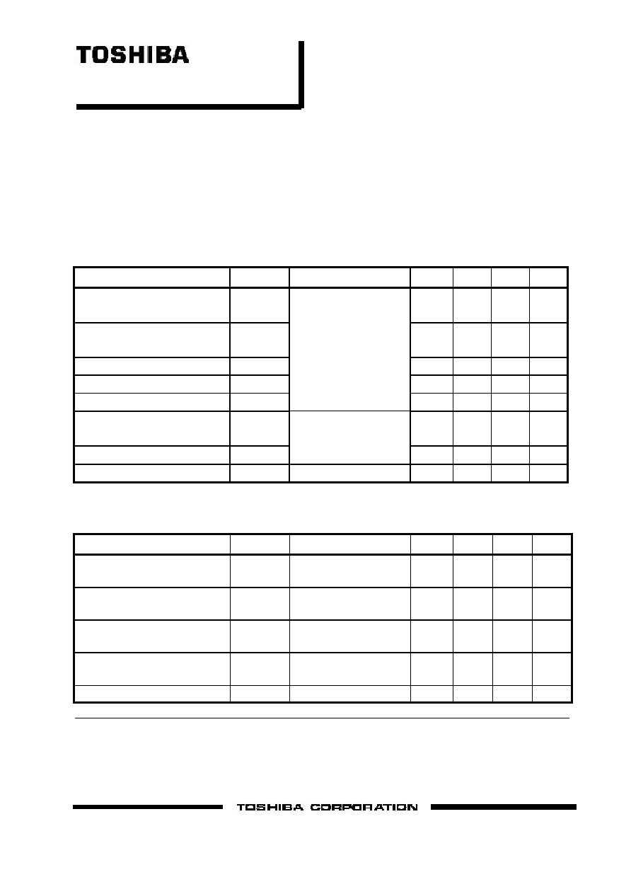
RF PERFORMANCE SPECIFICATIONS ( Ta= 25
�
C )
CHARACTERISTICS
SYMBOL
CONDITIONS
UNIT
MIN. TYP. MAX.
Output Power at 1dB Gain
Compression Point
P
1dB
dBm
45.0
45.5
Power Gain at 1dB Gain
Compression Point
G
1dB
dB
5.0
6.0
Drain Current
I
DS1
A
8.0
9.0
Gain Flatness
G
dB
�
0.8
Power Added Efficiency
add
V
DS
=10
V
f
= 7.7 to 8.5GHz
%
33
3rd Order Intermodulation
Distortion
IM
3
dBc
-42
-45
Drain Current
I
DS2
Two-Tone Test
Po=35.0dBm
(Single Carrier Level)
A
8.0
9.0
Channel Temperature Rise
Tch
V
DS
X I
DS
X R
th(c-c)
�
C
100
Recommended Gate Resistance(Rg): 28
(Max.)
ELECTRICAL CHARACTERISTICS ( Ta= 25
�
C )
CHARACTERISTICS
SYMBOL
CONDITIONS
UNIT
MIN.
TYP. MAX.
Transconductance
gm
V
DS
=
3V
I
DS
= 10.5A
mS
6500
Pinch-off Voltage
V
GSoff
V
DS
=
3V
I
DS
= 140mA
V
-1.0
-2.5
-4.0
Saturated Drain Current
I
DSS
V
DS
=
3V
V
GS
= 0V
A
20
26
Gate-Source Breakdown
Voltage
V
GSO
I
GS
= -420
�
A
V
-5
Thermal Resistance
R
th(c-c)
Channel to Case
�
C/W
1.0
1.3
u
The information contained herein is presented only as a guide for the applications of our products. No responsibility is
assumed by TOSHIBA for any infringements of patents or other rights of the third parties which may results from its use,
No license is granted by implication or otherwise under any patent or patent rights of TOSHIBA or others.
The information contained herein is subject to change without prior notice. It is therefor advisable to contact TOSHIBA
before proceeding with design of equipment incorporating this product.
Rev. Nov. 2003
2
TIM7785-35SL
ABSOLUTE MAXIMUM RATINGS ( Ta= 25
�
C )
CHARACTERISTICS
SYMBOL
UNIT
RATING
Drain-Source Voltage
V
DS
V
15
Gate-Source Voltage
V
GS
V
-5
Drain Current
I
DS
A
26
Total Power Dissipation (Tc= 25
�
C)
P
T
W
115
Channel Temperature
T
ch
�
C
175
Storage
T
stg
�
C
-65 to +175
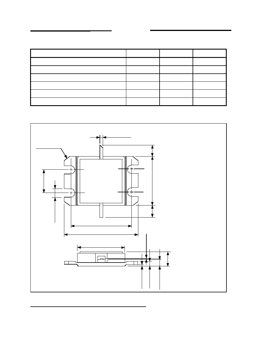
PACKAGE OUTLINE (2-16G1B)
Unit in mm
�
Gate
,
Source
Drain
HANDLING PRECAUTIONS FOR PACKAGE MODEL
Soldering iron should be grounded and the operating time should not exceed 10 seconds
at 260
�
C.
5.5 MAX.
0.2 MAX.
0.7
�
0.15
2.4
�
0.3
8.0
�
0.2
1.4
�
0.3
0.1
+0.1
-
0.05
2.5 MIN.
2.5 MIN.
17.4
�
0.4
2.6
�
0.3
20.4
�
0.3
24.5 MAX.
4
�
C1.0
�
,
,
16.4 MAX.

4
TIM7785-35SL
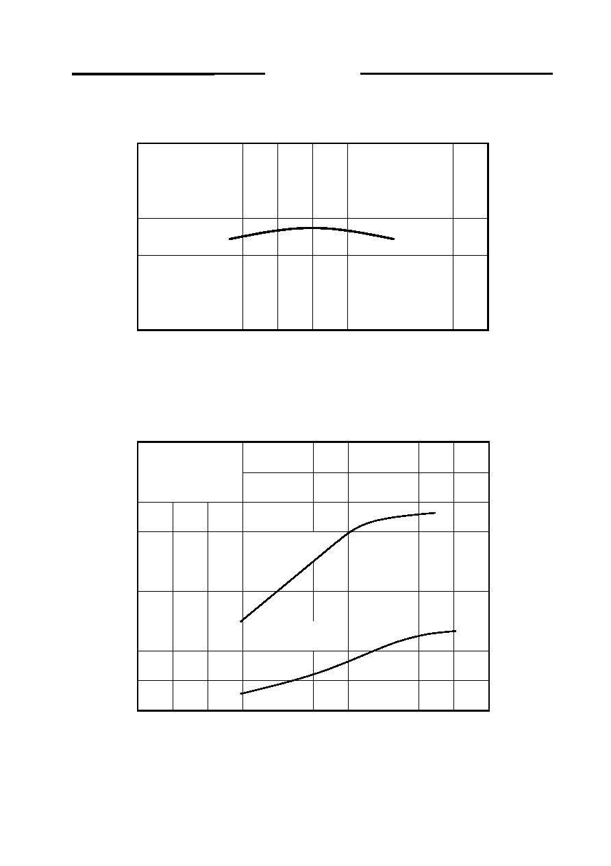
Power Dissipation(PT) vs. Case Temperature(Tc)
Tc(
�
C )
IM3 vs. Output Power Characteristics
VDS=10V
freq.=8.5GHz
f=5MHz
Pout(dBm) @Single carrier level
30
-10
-20
-30
-40
-50
-60
IM3(
dBc)
0
PT(W)
120
100
80
60
40
20
40
80
120
160
200
32
34
36
38
40
5
TIM7785-35SL
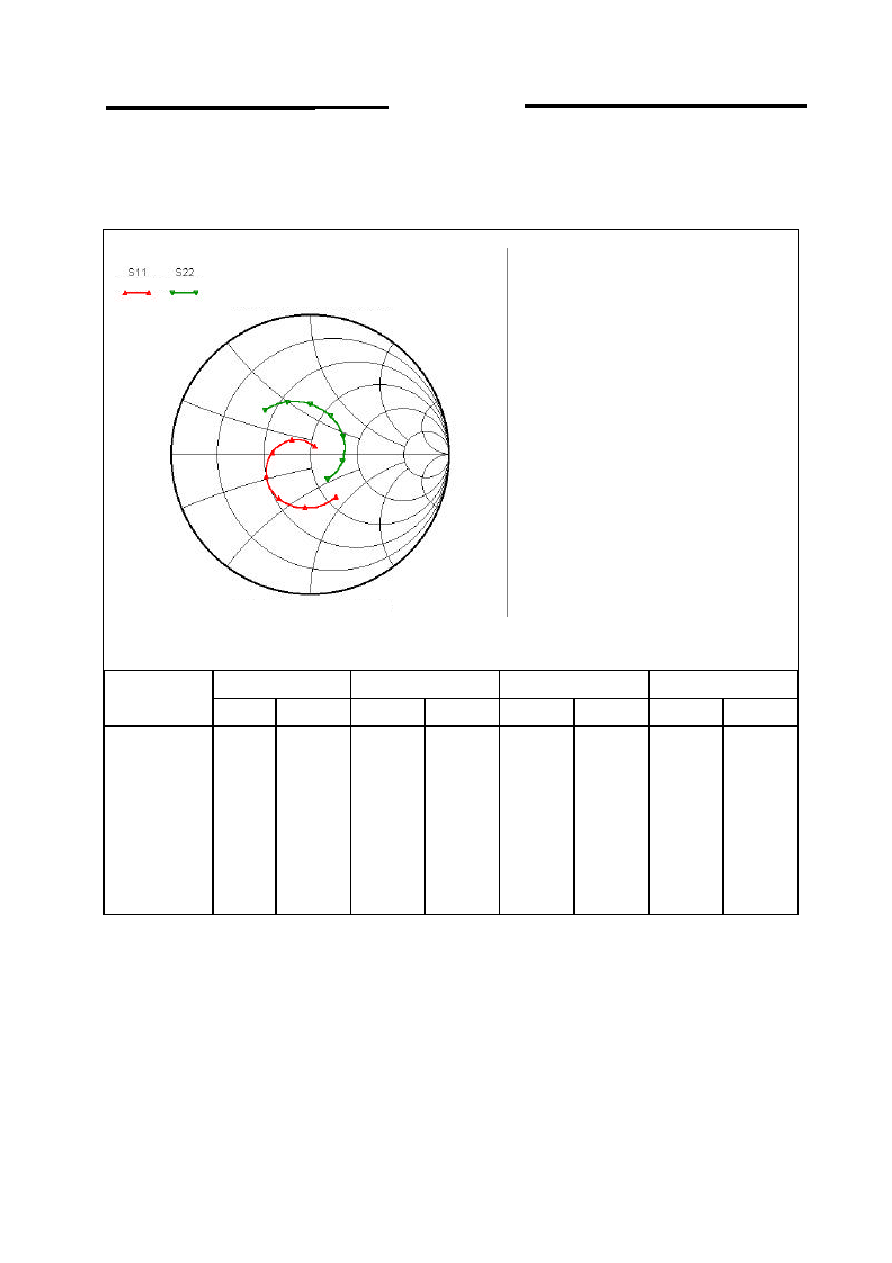
TIM7785-35SL S-PARAMETERS
(MAGN. and ANGLES)
V
DS
=10V, I
DS
=8.0A
S11
S12
S21
S22
FREQUENCY
(GHz)
MAG
ANG
MAG
ANG
MAG
ANG
MAG
ANG
7.50
-8.9814 -58.883
7.7466 -132.94 -26.718 -157.88
-6.814
135.77
7.70
-8.3276 -95.847
7.6201
178.84
-26.03
153.1 -7.7217
113.8
7.00
-8.2456 -125.79
7.5867
131.47 -25.415
105.53 -8.8479
90.07
8.10
-9.079 -153.45
7.6876
83.846 -24.785
58.534 -10.106
62.308
8.30
-11.201
177.35
7.8387
35.074 -24.184
10.528 -11.394
28.383
8.50
-15.55
141.44
7.9431 -15.135 -23.802 -38.853 -12.511
-11.132
8.70
-23.587
61.355
7.8793 -66.763 -23.776 -89.791
-13.44
-55.383
7.5
7.7
7.9
8.1
8.3
8.5
8.7
8.7
8.5
8.3
8.1
7.9
7.7
7.5
f=7.5 to 8.7 GHz