TG2210FT
2002-07-30
1
TOSHIBA GaAs Linear Integrated Circuit GaAs Monolithic
TG2210FT
RF SPDT Switch
Switch the receive filter for mobile communication.
Switch the diversity antenna.
Switch the local signal.
Features
· Low insertion Loss: L
OSS
= 0.4dB (typ.)
· High isolation: ISL = 30dB (typ.)
· Low voltage operation: V
C
= 0 V/2.5 V
· Small package: TU6 package (2.0 × 1.25 × 0.6 mm)
Pin Connection, Marking
(top view)
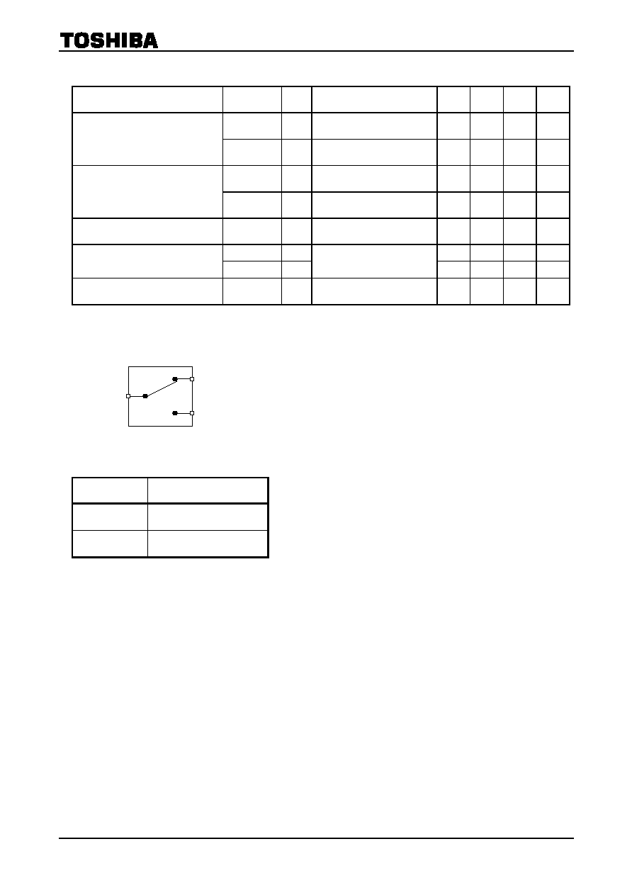
Maximum Ratings
(Ta
=
=
=
=
25°C)
Characteristics Symbol
Rating
Unit
V
C1
5 V
Control voltage
V
C2
5 V
Input power
P
i
1
W
Operating temperature range
T
opr
-
40~85 °C
Storage temperature range
T
stg
-
55~125 °C
Caution
This device is sensitive to electrostatic discharge. When using this device, please ensure that all tools and
equipment are earthed.
Weight: 0.008 g (typ.)
U L
6 4
1 2 3
5
RF2 GND RF1
V
C1
RFcom V
C2
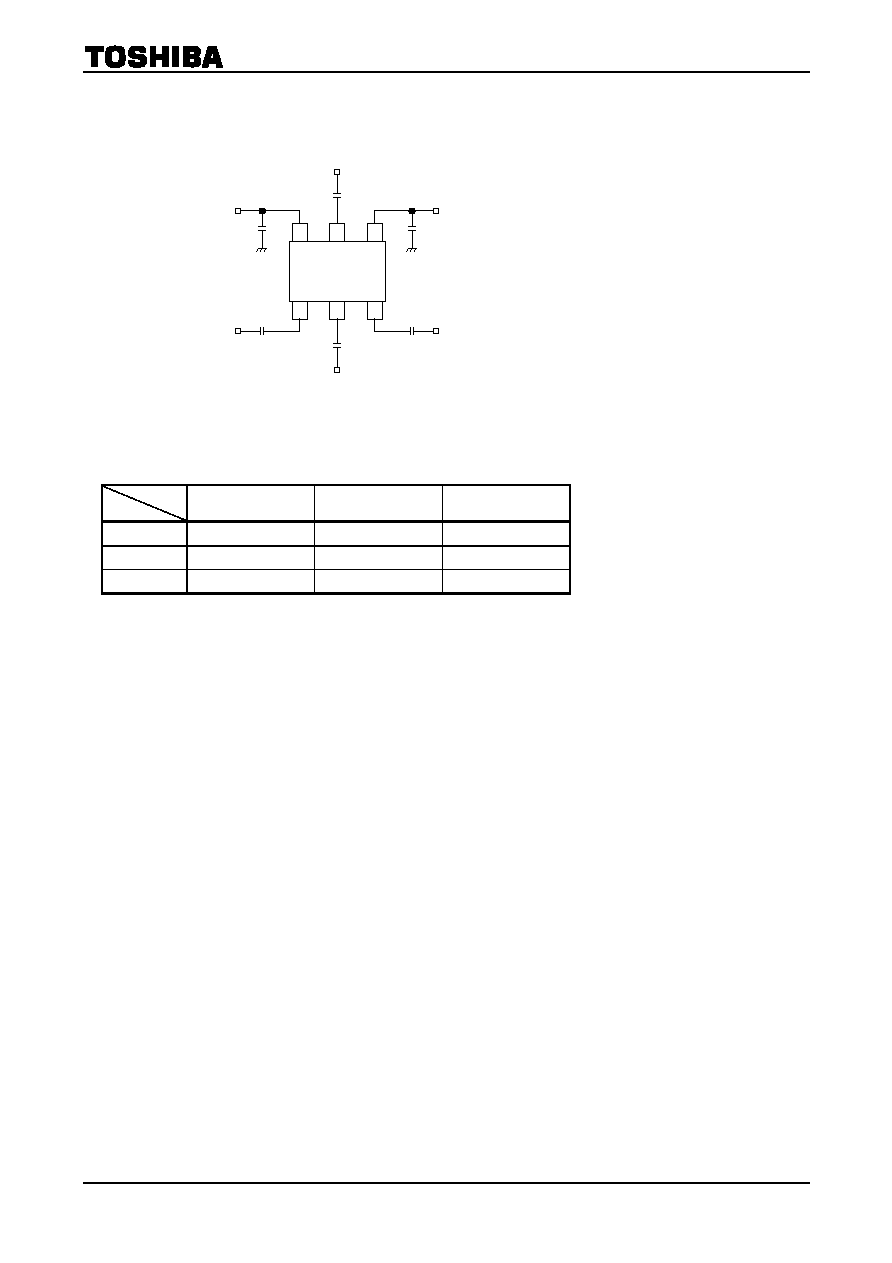
TG2210FT
2002-07-30
3
Test Circuit 1
(RF Test Circuit)
Please fix the value of each capacity for using frequency and circuit.
Recommend Capacity
1 GHz
1.6 GHz
2.4 GHz
1
100 pF
100 pF
100 pF
2
100 pF
100 pF
100 pF
3
7 pF
3 pF
1.5 pF
Notice
The circuits and measurements contained in this document are given only in the context of as examples of
applications for these products.
Moreover, these example application circuits are not intended for mass production, since the high-frequency
characteristics (the AC characteristics) of these devices will be affected by the external components which the
customer uses, by the design of the circuit and by various other conditions.
It is the responsibility of the customer to design external circuits which correctly implement the intended
application, and to check the characteristics of the design.
TOSHIBA assume no responsibility for the integrity of customer circuit designs or applications.
C
1
C
2
RF2
Top
view
V
C1
C
1
RF1
C
3
GND
C1
RFcom
V
C2
C
2
C
1
: 100 pF
C
2
: 100 pF
C
3
: 7 pF
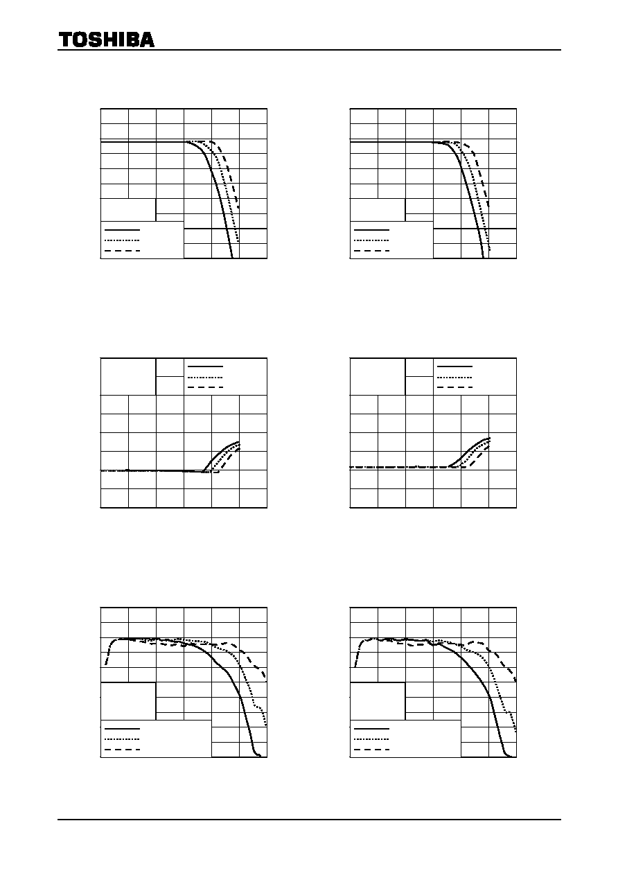
TG2210FT
2002-07-30
4
L
OSS
(1)
-
P
i
L
OSS
(2)
-
P
i
ISL (1)
-
P
i
ISL (2)
-
P
i
L
OSS
(1)
-
f
L
OSS
(2)
-
f
Input power P
i
(dBmW)
Input power P
i
(dBmW)
Input power P
i
(dBmW)
Input power P
i
(dBmW)
Frequency f (GHz)
Frequency f (GHz)
In
se
r
t
io
n
lo
s
s
L
OSS
(2
) (d
B
)
In
se
r
t
io
n
lo
s
s
L
OSS
(1
) (d
B
)
Isol
ati
on
IS
L
(2)
(
d
B
)
Isol
ati
on
IS
L
(1)
(
d
B
)
In
se
r
t
io
n
lo
s
s
L
OSS
(2
) (d
B
)
In
se
r
t
io
n
lo
s
s
L
OSS
(1
) (d
B
)
2.0
0 10 20 30
1.0
0.0
VC1
=
2.5 V
VC1
=
2.7 V
VC1
=
3.0 V
VC2
=
0 V
f
=
1.0 GHz
2.0
0
10
20 30
1.0
0.0
VC2
=
2.5 V
VC2
=
2.7 V
VC2
=
3.0 V
VC1
=
0 V
f
=
1.0 GHz
40
0
10
20 30
30
0
VC2
=
2.5 V
VC2
=
2.7 V
VC2
=
3.0 V
VC1
=
0 V
f
=
1.0 GHz
20
10
2.0
0.0 1.0 2.0 3.0
1.0
0.0
1.0 GHz matching
1.6 GHz matching
2.4 GHz matching
VC1
=
2.5 V
VC2
=
0 V
Pi
=
0dBmW
2.0
0.0
1.0
2.0 3.0
1.0
0.0
1.0 GHz matching
1.6 GHz matching
2.4 GHz matching
VC1
=
0 V
VC2
=
2.5 V
Pi
=
0dBmW
40
0 10 20 30
30
0
VC1
=
2.5 V
VC1
=
2.7 V
VC1
=
3.0 V
VC2
=
0 V
f
=
1.0 GHz
20
10
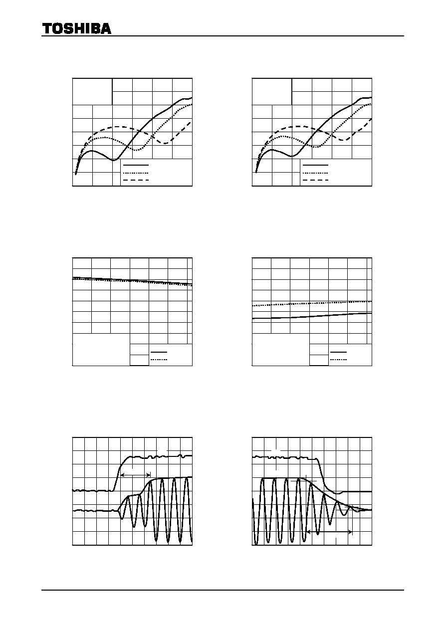
TG2210FT
2002-07-30
5
ISL (1)
-
f
ISL (2)
-
f
L
OSS
(1), (2)
-
Ta
ISL (1), (2)
-
Ta
Switching Time (RAISE)
Switching Time (FALL)
Frequency f (GHz)
Frequency f (GHz)
Temperature Ta (°C)
Temperature Ta (°C)
Time (10 ns/div)
Time (10 ns/div)
Isol
ati
on
IS
L
(2)
(
d
B
)
Isol
ati
on
IS
L
(1)
(
d
B
)
Isol
ati
on
IS
L
(1)
,
(
2
)
(dB
)
In
se
r
t
io
n
lo
s
s
L
OSS
(1
),
(2
)
(
d
B
)
40
0.0 1.0 2.0 3.0
30
0
1.0 GHz matching
1.6 GHz matching
2.4 GHz matching
VC1
=
2.5 V
VC2
=
0 V
Pi
=
0dBmW
20
10
40
0.0
1.0
2.0 3.0
30
0
1.0 GHz matching
1.6 GHz matching
2.4 GHz matching
VC1
=
0 V
VC2
=
2.5 V
Pi
=
0dBmW
20
10
35.0
-
40
0
-
20
80
31.0
25.0
ISL (1) ISL
(2)
VC1
=
2.5 V VC1
=
0 V
VC2
=
0 V
VC2
=
2.5 V
Pi
=
0dBmW, f
=
1.0 GHz
20
40 60
ISL (1)
ISL (2)
27.0
29.0
33.0
2.0
-
40 0
-
20 80
1.0
0.0
LOSS (1) LOSS (2)
VC1
=
2.5 V VC1
=
0 V
VC2
=
0 V
VC2
=
2.5 V
Pi
=
0dBmW, f
=
1.0 GHz
20
40 60
LOSS (1)
LOSS (2)
VC
RF
23 ns
RF
39 ns
VC