
2SK3373
2002-09-02
1
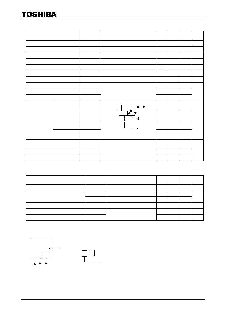
TOSHIBA Field Effect Transistor Silicon N Channel MOS Type (-MOSV)
2SK3373
Switching Regulator and DC-DC Converter Applications
Motor Drive Applications
· Low drain-source ON resistance: R
DS (ON)
= 2.9 m (typ.)
· High forward transfer admittance: |Y
fs
| = 1.7 S (typ.)
· Low leakage current: I
DSS
= 100 µA (max) (V
DS
= 500 V)
· Enhancement-model: V
th
= 2.0 to 4.0 V (V
DS
= 10 V, I
D
= 1 mA)
Maximum Ratings
(Ta
=
=
=
=
25°C)
Characteristics Symbol
Rating
Unit
Drain-source voltage
V
DSS
500 V
Drain-gate voltage (R
GS
= 20 kW) V
DGR
500 V
Gate-source voltage
V
GSS
±30 V
DC (Note
1) I
D
2
Pulse (t
= 1 ms)
(Note
1)
I
DP
5
Drain current
Pulse (t
= 100 ms)
(Note
1)
I
DP
12
A
Drain power dissipation (Tc
= 25°C)
P
D
20 W
Single pulse avalanche energy
(Note
2)
E
AS
112 mJ
Avalanche current
I
AR
2
A
Repetitive avalanche energy (Note 3)
E
AR
2
mJ
Channel temperature
T
ch
150
°C
Storage temperature range
T
stg
-55 to150
°C
Thermal Characteristics
Characteristics Symbol
Max
Unit
Thermal resistance, channel to case
R
th (ch-c)
6.25
°C/W
Thermal resistance, channel to ambient
R
th (ch-a)
125
°C/W
Note 1: Please use devices on condition that the channel temperature is below 150°C.
Note 2: V
DD
= 90 V, T
ch
= 25°C (initial), L = 48.4 mH, R
G
= 25 W, I
AR
= 2 A
Note 3: Repetitive rating: pulse width limited by maximum channel temperature
This transistor is an electrostatic sensitive device. Please handle with caution.
Unit: mm
JEDEC
JEITA
TOSHIBA 2-7J1B
Weight: 0.36 g (typ.)
2SK3373
2002-09-02
2
Electrical Characteristics
(Ta
=
=
=
=
25°C)
Characteristics Symbol Test
Condition Min
Typ.
Max
Unit
Gate leakage current
I
GSS
V
GS
= ±25 V, V
DS
= 0 V
ľ
ľ
±10
mA
Drain-source breakdown voltage
V
(BR) GSS
I
G
= ±10 mA, V
DS
= 0 V
±30
ľ
ľ
V
Drain cut-OFF current
I
DSS
V
DS
= 500 V, V
GS
= 0 V
ľ
ľ
100
mA
Drain-source breakdown voltage
V
(BR) DSS
I
D
= 10 mA, V
GS
= 0 V
500
ľ
ľ
V
Gate threshold voltage
V
th
V
DS
= 10 V, I
D
= 1 mA
2.0
ľ
4.0 V
Drain-source ON resistance
R
DS (ON)
V
GS
= 10 V, I
D
= 1 A
ľ
2.9 3.2
W
Forward transfer admittance
ďY
fs
ď
V
DS
= 10 V, I
D
= 1 A
0.8
1.7
ľ
S
Input capacitance
C
iss
ľ
380
ľ
Reverse transfer capacitance
C
rss
ľ
40
ľ
Output capacitance
C
oss
V
DS
= 10 V, V
GS
= 0 V, f = 1 MHz
ľ
120
ľ
pF
Rise time
t
r
ľ
15
ľ
Turn-ON time
t
on
ľ
25
ľ
Fall time
t
f
ľ
20
ľ
Switching time
Turn-OFF time
t
off
ľ
80
ľ
ns
Total gate charge
(gate-source plus gate-drain)
Q
g
ľ
9
ľ
Gate-source charge
Q
gs
ľ
5
ľ
Gate-drain ("miller") charge
Q
gd
V
DD
~
- 400 V, V
GS
= 10 V, I
D
= 2 A
ľ
4
ľ
nC
Source-Drain Ratings and Characteristics
(Ta
=
=
=
=
25°C)
Characteristics Symbol
Test
Condition
Min
Typ.
Max
Unit
Continuous drain reverse current (Note 1)
I
DR
ľ
ľ
ľ 2 A
I
DRP
t
= 1 ms
ľ
ľ 5
Pulse drain reverse current
(Note 1)
I
DRP
t
= 100 ms
ľ
ľ 12
A
Forward voltage (diode)
V
DSF
I
DR
= 2 A, V
GS
= 0 V
ľ
ľ
-1.5
V
Reverse recovery time
t
rr
ľ 1000 ľ ns
Reverse recovery charge
Q
rr
I
DR
= 2 A, V
GS
= 0 V,
dI
DR
/dt
= 100 A/ms
ľ 3.5 ľ
mC
Marking
Type
K3373
Lot Number
Month (starting from alphabet A)
Year
(last number of the christian era)
Duty <= 1%, t
w
= 10 ms
0 V
10
V
V
GS
R
L
= 200 W
V
DD
~
- 200 V
I
D
= 1 A
V
OUT
50
9
2SK3373
2002-09-02
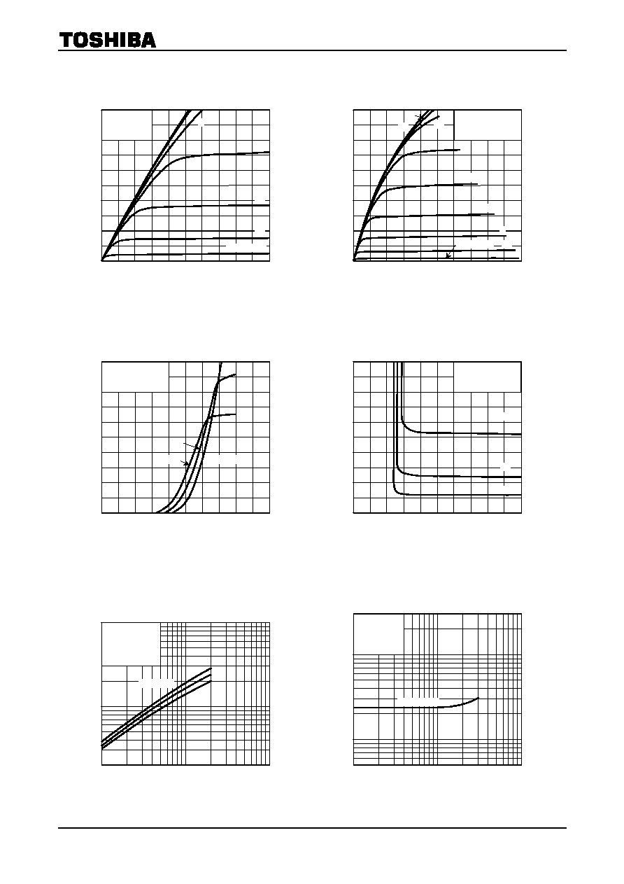
3
Fo
rw
ar
d t
r
a
n
sfe
r
ad
mi
ttanc
e
ď
Y
fs
ď
(
S
)
D
r
ai
n
-
so
urc
e
v
o
l
t
a
ge
V
DS
(V
)
Drain-source voltage V
DS
(V)
I
D
V
DS
D
r
ai
n
cu
rre
nt
I
D
(A
)
Drain-source voltage V
DS
(V)
I
D
V
DS
D
r
ai
n
cu
rre
nt
I
D
(A
)
Gate-source voltage V
GS
(V)
I
D
- V
GS
D
r
ai
n
cu
rre
nt
I
D
(A
)
Gate-source voltage V
GS
(V)
V
DS
- V
GS
Drain current I
D
(A)
ďY
fs
ď - I
D
Drain current I
D
(A)
R
DS (ON)
- I
D
D
r
ai
n
-
so
urc
e
on resi
s
t
a
n
ce
R
DS (ON)
(
W
)
0
2.0
0.4
1.2
0.8
1.6
2
0
10
4 6 8
Common source
Tc
= 25°C
pulse test
VGS = 4 V
5
5.5
10 8
6
4.5
0
10
2
6
4
8
4
0
20
8
12 16
0.5
Common source
Tc
= 25°C
pulse test
1
ID = 2 A
Common source
VDS = 20 V
pulse test
0
5
1
3
2
4
2
0
10
4 6 8
Tc
= -55°C
25
100
Common source
Tc
= 25°C
pulse test
0
5
1
3
2
4
10
0
50
20
30 40
VGS = 4 V
5
4.5
10
7
5.5
6
6.5
8
25
0.2
0.1
10
10
3
1
0.3
0.5
0.5 1
3
5
0.3
Common source
VDS = 20 V
pulse test
Tc
= -55°C
100
5
0.1 1
0.3 0.5
3 5
1
10
5
30
3
0.5
Common source
Tc
= 25°C
Pulse test
10
VGS = 10 V

2SK3373
2002-09-02
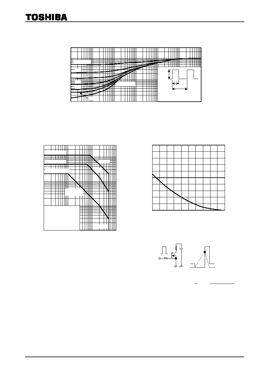
4
D
r
ai
n
po
w
e
r
di
ssi
p
a
ti
on
P
D
(W
)
Gate
th
res
hol
d vol
t
a
ge
V
th
(V
)
Case temperature Tc (°C)
RDS (ON) - Tc
D
r
ai
n
-
so
urc
e
on resi
s
t
a
n
ce
R
DS (ON)
(
W
)
Drain-source voltage V
DS
(V)
IDR - VDS
D
r
ai
n
re
ver
s
e c
u
r
r
e
n
t
I
DR
(A
)
Drain-source voltage V
DS
(V)
Capacitance VDS
C
apaci
t
anc
e C
(p
F)
Case temperature Tc (°C)
V
th
- Tc
Case temperature Tc (°C)
P
D
- Tc
D
r
ai
n
-
so
urc
e
v
o
l
t
a
ge
V
DS
(V
)
Gate
-so
u
r
c
e
v
o
l
t
age
V
GS
(V
)
Total gate charge Q
g
(nC)
Dynamic input/output characteristics
10
1000
30
100
1
0.1 100
10
Ciss
Coss
Crss
Common source
VGS = 0 V
f
= 1 MHz
Tc
= 25°C
2
5
50
300
500
0.3 0.5
3
5
30 50
5
1
3
2
4
0
-80
0
40
80
120
160
-40
Common source
VDS = 10 V
ID = 1 mA
pulse test
2.0
0.4
1.2
0.8
1.6
0
0
80
120
200
40
160
500
100
300
200
400
0
0
8
12
16
20
4
Common source
ID = 2 A
Tc = 25°C
pulse test
200
VDD = 400 V
VDS
VGS
20
4
12
8
16
0
100
0.01
10
0.03
0.3
3
-0.2
0
-1.2
-0.6
-0.4
-0.8
-1.0
10
3
1
VGS = 0, -1 V
1
0.1
Common source
Tc
= 25°C
pulse test
0
10
2
6
4
8
-40
-80
160
0 40 80
Common source
VGS = 10 V
pulse test
ID = 2 A
0.5
1
2SK3373
2002-09-02
5
r
th
- t
w
Safe operating area
E
AS
- T
ch
Pulse width t
w
(S)
Channel temperature (initial) Tch (°C)
N
o
r
m
al
i
z
ed t
r
a
n
si
e
n
t t
h
e
r
m
a
l
i
m
pe
da
nc
e
r th (t)
/R
th
(c
h-c
)
A
v
al
anc
he
en
er
gy E
AS
(
m
J)
D
r
ai
n
cu
rre
nt
I
D
(A
)
-15 V
15
V
Test circuit
Wave form
I
AR
B
VDSS
V
DD
V
DS
R
G
= 25 W
V
DD
= 90 V, L = 48.4 mH
÷
÷
ř
ö
ç
ç
č
ć
-
×
×
×
=
VDD
BVDSS
BVDSS
2
I
L
2
1
AS
0.01
0.1
1
3
0.3
0.03
10
m 100
m
1 m
10 m
100 m
1
T
PDM
t
Duty
= t/T
Rth (ch-c) = 6.25°C/W
Duty
= 0.5
0.2
0.1
Single Pulse
0.05
0.02
0.01
10
Drain-source voltage V
DS
(V)
0
25
40
80
120
200
160
50
75
100 125 150
00.1
1
0.1
1
10
30
10 100
1000
*: Single nonrepetitive pulse
Tc
= 25°C
Curves must be derated
linearly with increase in
temperature.
ID max (continuous)
ID max (pulsed) *
100
ms *
DC operation
Tc
= 25°C
1 ms *
VDSS max
3
00.3
0.3
ID max (pulsed) *