UC1526
UC2526
UC3526
DESCRIPTION
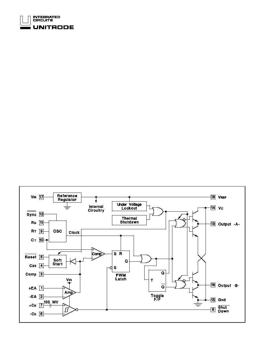
The UC1526 is a high performance monolithic pulse width modulator
circuit designed for fixed-frequency switching regulators and other
power control applications. Included in an 18-pin dual-in-line pack-
age are a temperature compensated voltage reference, sawtooth os-
cillator, error amplifier, pulse width modulator, pulse metering and
setting logic, and two low impedance power drivers. Also included
are protective features such as soft-start and under-voltage lockout,
digital current limiting, double pulse inhibit, a data latch for single
pulse metering, adjustable deadtime, and provision for symmetry cor-
rection inputs. For ease of interface, all digital control ports are TTL
and B-series CMOS compatible. Active LOW logic design allows
wired-OR connections for maximum flexibility. This versatile device
can be used to implement single-ended or push-pull switching regu-
lators of either polarity, both transformerless and transformer cou-
pled. The UC1526 is characterized for operation over the full military
temperature range of -55°C to +125°C. The UC2526 is characterized
for operation from -25°C to +85°C, and the UC3526 is characterized
for operation from 0° to +70°C.
Regulating Pulse Width Modulator
FEATURES
·
8 To 35V Operation
·
5V Reference Trimmed To
±
1%
·
1Hz To 400kHz Oscillator Range
·
Dual 100mA Source/Sink Outputs
·
Digital Current Limiting
·
Double Pulse Suppression
·
Programmable Deadtime
·
Under-Voltage Lockout
·
Single Pulse Metering
·
Programmable Soft-Start
·
Wide Current Limit Common Mode Range
·
TTL/CMOS Compatible Logic Ports
·
Symmetry Correction Capability
·
Guaranteed 6 Unit Synchronization
BLOCK DIAGRAM
6/93

ABSOLUTE MAXIMUM RATINGS (Note 1, 2)
Input Voltage (+V
IN
) . . . . . . . . . . . . . . . . . . . . . . . . . . . . . . +40V
Collector Supply Voltage (+V
C
) . . . . . . . . . . . . . . . . . . . . . +40V
Logic Inputs . . . . . . . . . . . . . . . . . . . . . . . . . . . . . -0.3V to +5.5V
Analog Inputs . . . . . . . . . . . . . . . . . . . . . . . . . . . . . -0.3V to +V
IN
Source/Sink Load Current (each output) . . . . . . . . . . . . . 200mA
Reference Load Current . . . . . . . . . . . . . . . . . . . . . . . . . . . 50mA
Logic Sink Current . . . . . . . . . . . . . . . . . . . . . . . . . . . . . . . 15mA
Power Dissipation at T
A
= +25°C (Note 2) . . . . . . . . . . 1000mW
Power Dissipation at T
C
= +25°C (Note 2) . . . . . . . . . . 3000mW
Operating Junction Temperature . . . . . . . . . . . . . . . . . . +150°C
Storage Temperature Range . . . . . . . . . . . . . . -65°C to +150°C
Lead Temperature (soldering, 10 seconds) . . . . . . . . . . +300°C
Note 1: Values beyond which damage may occur.
Note 2: Consult packaging section of databook for thermal
limitations and considerations of package.
CONNECTION DIAGRAMS
UC1526
UC2526
UC3526
DIL-18, SOIC-18 (TOP VIEW)
J or N Package, DW Package
RECOMMENDED OPERATING CONDITIONS (Note 3)
Input Voltage . . . . . . . . . . . . . . . . . . . . . . . . . . . . . . +8V to +35V
Collector Supply Voltage . . . . . . . . . . . . . . . . . . . +4.5V to +35V
Sink/Source Load Current (each output) . . . . . . . . . 0 to 100mA
Reference Load Current . . . . . . . . . . . . . . . . . . . . . . 0 to 20mA
Oscillator Frequency Range . . . . . . . . . . . . . . . . 1Hz to 400kHz
Oscillator Timing Resistor . . . . . . . . . . . . . . . . . . . 2k
to 150k
Oscillator Timing Capacitor . . . . . . . . . . . . . . . . . . . 1nF to 20
µ
F
Available Deadtime Range at 40kHz . . . . . . . . . . . . . 3% to 50%
Operating Ambient Temperature Range
UC1526 . . . . . . . . . . . . . . . . . . . . . . . . . . . . -55°C to +125°C
UC2526 . . . . . . . . . . . . . . . . . . . . . . . . . . . . . -25°C to +85°C
UC3526 . . . . . . . . . . . . . . . . . . . . . . . . . . . . . . -0°C to +70°C
Note 3: Range over which the device is functional and
parameter limits are guaranteed.
PACKAGE PIN FUNCTION
FUNCTION
PIN
N/C
1
+Error
2
-Error
3
Comp.
4
C
SS
5
Reset
______
6
- Current Sense
7
+ Current Sense
8
Shutdown
_________
9
R
TIMING
10
C
T
11
R
D
12
Sync
13
Output A
14
V
C
15
N/C
16
Ground
17
Output B
18
+V
IN
19
V
REF
20
PLCC-20, LCC-20
(TOP VIEW)
Q and L Packages
ELECTRICAL CHARACTERISTICS:
PARAMETER
TEST CONDITIONS
UC1526 / UC2526
UC3526
UNITS
MIN
TYP
MAX
MIN
TYP
MAX
Reference Section (Note 4)
Output Voltage
T
J
= + 25°C
4.95
5.00
5.05
4.90
5.00
5.10
V
Line Regulation
+V
IN
= 8 to 35V
10
20
10
30
mV
Load Regulation
I
L
= 0 to 20mA
10
30
10
50
mV
Temperature Stability
Over Operating T
J
15
50
15
50
mV
Total Output
Voltage Range
Over Recommended
Operating Conditions
4.90
5.00
5.10
4.85
5.00
5.15
V
Short Circuit Current
V
REF
= 0V
25
50
100
25
50
100
mA
Under -Voltage Lockout
RESET
_______
Output Voltage
V
REF
= 3.8V
0.2
0.4
0.2
0.4
V
V
REF
= 4.8V
2.4
4.8
2.4
4.8
V
Note 4: I
L
= 0mA.
+V
IN
= 15V, and over operating ambient temperature, unless otherwise
specified, T
A
= T
J.
2

ELECTRICAL CHARACTERISTICS:
PARAMETER
TEST CONDITIONS
UC1526 / UC2526
UC3526
UNITS
MIN
TYP
MAX
MIN
TYP
MAX
Oscillator Section (Note 5)
Initial Accuracy
T
J
= + 25°C
±
3
±
8
±
3
±
8
%
Voltage Stability
+V
IN
= 8 to 35V
0.5
1
0.5
1
%
Temperature Stability
Over Operating T
J
7
10
3
5
%
Minimum Frequency
R
T
= 150k
, C
T
= 20
µ
µ
F
1
1
Hz
Maximum Frequency
R
T
= 2k
, C
T
= 1.0nF
400
400
kHz
Sawtooth Peak Voltage
+V
IN
= 35V
3.0
3.5
3.0
3.5
V
Sawtooth Valley Voltage
+V
IN
= 8V
0.5
1.0
0.5
1.0
V
Error Amplifier Section (Note 6)
Input Offset Voltage
R
S
2k
2
5
2
10
mV
Input Bias Current
-350
-1000
-350
-2000
nA
Input Offset Current
35
100
35
200
nA
DC Open Loop Gain
R
L
10M
64
72
60
72
dB
HIGH Output Voltage
V
PIN1
-V
PIN2
150mV, I
SOURCE
=
100
µ
µ
A
3.6
4.2
3.6
4.2
V
LOW Output Voltage
V
PIN2
-V
PIN1
150mV, I
SINK
=
100
µ
µ
A
0.2
0.4
0.2
0.4
V
Common Mode Rejection
Rs
12k
70
94
70
94
dB
Supply Voltage Rejection
+V
IN
= 12 to 18V
66
80
66
80
dB
PWM Comparator (Note 5)
Minimum Duty Cycle
V
COMPENSATION
= +0.4V
0
0
%
Maximum Duty Cycle
V
COMPENSATION
= +3.6V
45
49
45
49
%
Digital Ports (SYNC, SHUTDOWN, and RESET)
HIGH Output Voltage
I
SOURCE
=40
µ
µ
A
2.4
4.0
2.4
4.0
V
LOW Output Voltage
I
SINK
= 3.6mA
0.2
0.4
0.2
0.4
V
HIGH Input Current
V
IH
= +2.4V
-125
-200
-125
-200
µ
A
LOW Input Current
V
IL
= +0.4V
-225
-360
-225
-360
µ
A
Current LImit Comparator (Note 7)
Sense Voltage
R
S
50
90
100
110
80
100
120
mV
Input Bias Current
-3
-10
-3
-10
µ
A
Soft-Start Section
Error Clamp Voltage
RESET = +0.4V
0.1
0.4
0.1
0.4
V
Cs Charging Current
RESET =+2.4V
50
100
150
50
100
150
µ
A
Output Drivers (Each Output) (Note 8)
HIGH Output Voltage
I
SOURCE
= 20mA
12.5
13.5
12.5
13.5
V
I
SOURCE
= 100mA
12
13
12
13
V
LOW Output Voltage
I
SINK
= 20mA
0.2
0.3
0.2
0.3
V
I
SINK
= 100mA
1.2
2.0
1.2
2.0
V
Collector Leakage
V
C
= 40V
50
150
50
150
µ
A
Rise Time
C
L
= 1000pF
0.3
0.6
0.3
0.6
µ
s
Fall Time
C
L
= 1000pF
0.1
0.2
0.1
0.2
µ
s
Power Consumption (Note 9)
Standby Current
SHUTDOWN
____________
=
+
0.4V
18
30
18
30
mA
+V
IN
= 15V, and over operating ambient temperature, unless otherwise
specified, T
A
= T
J.
UC1526
UC2526
UC3526
Note 4: I
L
= 0mA.
Note 5: F
OSC
= 40kHz (R
T
= 4.12k
±
1%, C
T
= 0.1
µ
F
±
1%,
R
D
= 0
)
Note 6: V
CM
= 0 to +5.2V
Note 8: V
C
= +15V
Note 9: +V
IN
= +35V, R
T
= 4.12k
3
UC1526
UC2526
UC3526
APPLICATIONS INFORMATION
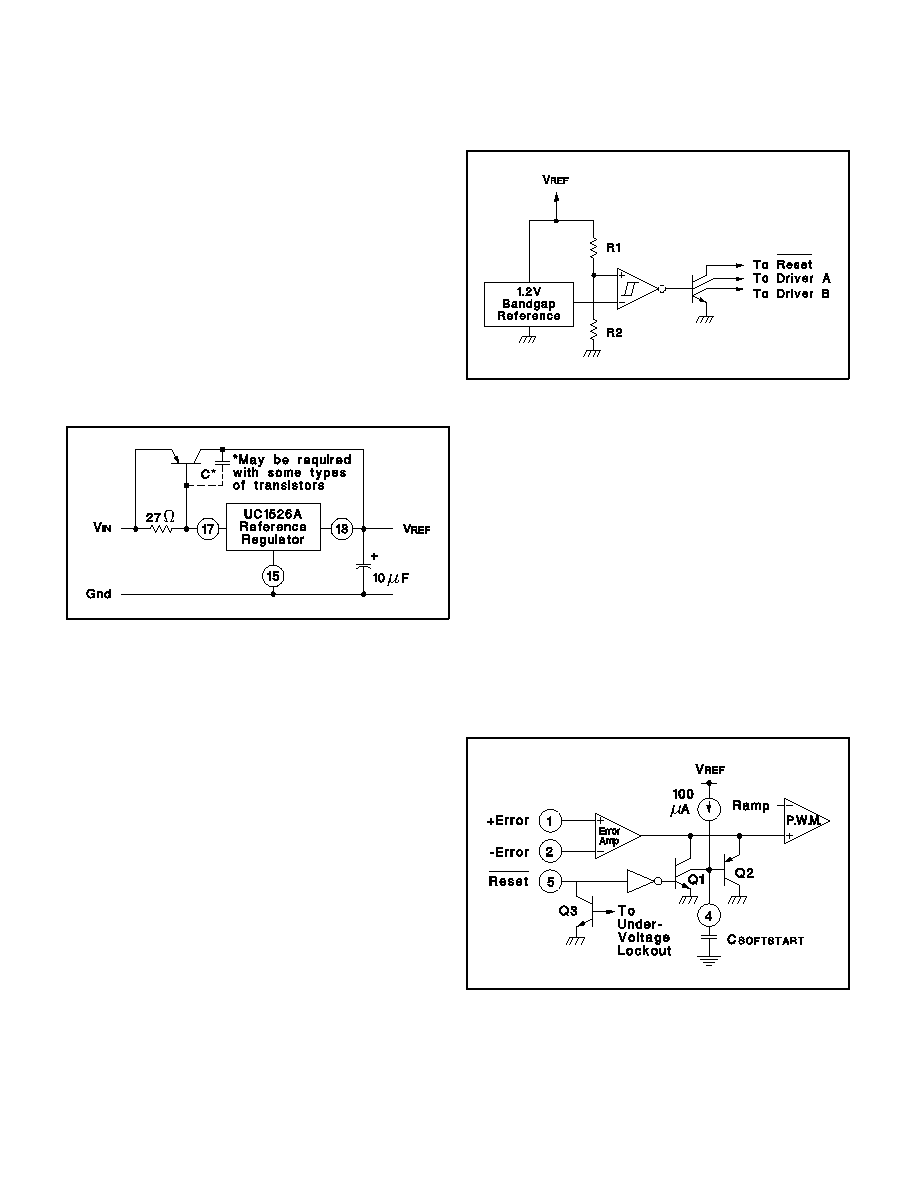
Voltage Reference
T
he reference regulator of the UC1526 is based on a tem-
perature compensated zener diode. The circuitry is fully
active at supply voltages above +8V, and provides up to
20mA of load current to external circuitry at +5.0V. In sys-
tems where additional current is required, an external
PNP transistor can be used to boost the available current.
A rugged low frequency audio-type transistor should be
used, and lead lengths between the PWM and transistor
should be as short as possible to minimize the risk of os-
cillations. Even so, some types of transistors may require
collector-base capacitance for stability. Up to 1 amp of
load current can be obtained with excellent regulation if
the device selected maintains high current gain.
Under-Voltage Lockout
The under-voltage lockout circuit protects the UC1526
and the power devices it controls from inadequate supply
voltage, If +V
IN
is too low, the circuit disables the output
drivers and holds the RESET
_______
pin LOW. This prevents
spurious output pulses while the control circuitry is stabi-
lizing, and holds the soft-start timing capacitor in a dis-
charged state.
The circuit consists of a +1.2V bandgap reference and
comparator circuit which is active when the reference
voltage has risen to 3V
BE
or +1.8V at 25°C. When the ref-
erence voltage rises to approximately +4.4V, the circuit
enables the output drivers and releases the RESET
_______
pin,
allowing a normal soft-start. The comparator has 200mV
of hysteresis to minimize oscillation at the trip point.
When +V
IN
to the PWM is removed and the reference
drops to +4.2V, the under-voltage circuit pulls RESET
_______
LOW again. The soft-start capacitor is immediately dis-
charged, and the PWM is ready for another soft-start cy-
cle.
The UC1526 can operate from a +5V supply by connect-
ing the V
REF
pin to the +V
IN
pin and maintaining the sup-
ply between +4.8 and +5.2V.
Soft-Start Circuit
The soft-start circuit protects the power transistors and
rectifier diodes from high current surges during power
supply turn-on. When supply voltage is first applied to the
UC1526, the under-voltage lockout circuit holds RESET
_______
LOW with Q
3
. Q
1
is turned on, which holds the soft-start
capacitor voltage at zero. The second collector of Q
1
clamps the output of the error amplifier to ground, guaran-
teeing zero duty cycle at the driver outputs. When the
supply voltage reaches normal operating range, RESET
_______
will go HIGH. Q
1
turns off, allowing the internal 100mA
current source to charge C
S
. Q
2
clamps the error ampli-
fier output to 1V
BE
above the voltage on C
S
. As the soft-
start voltage ramps up to +5V, the duty cycle of the PWM
linearly increases to whatever value the voltage regula-
tion loop requires for an error null.
Digital Control Ports
The three digital control ports of the UC1526 are bi-direc-
tional. Each pin can drive TTL and 5V CMOS logic di-
rectly, up to a fan-out of 10 low-power Schottky gates.
Each pin can also be directly driven by open-collector
Figure 2.
Under-Voltage Lockout Schematic
Figure 1.
Extending Reference Output Current
Figure 3.
Soft-Start Circuit Schematic
4
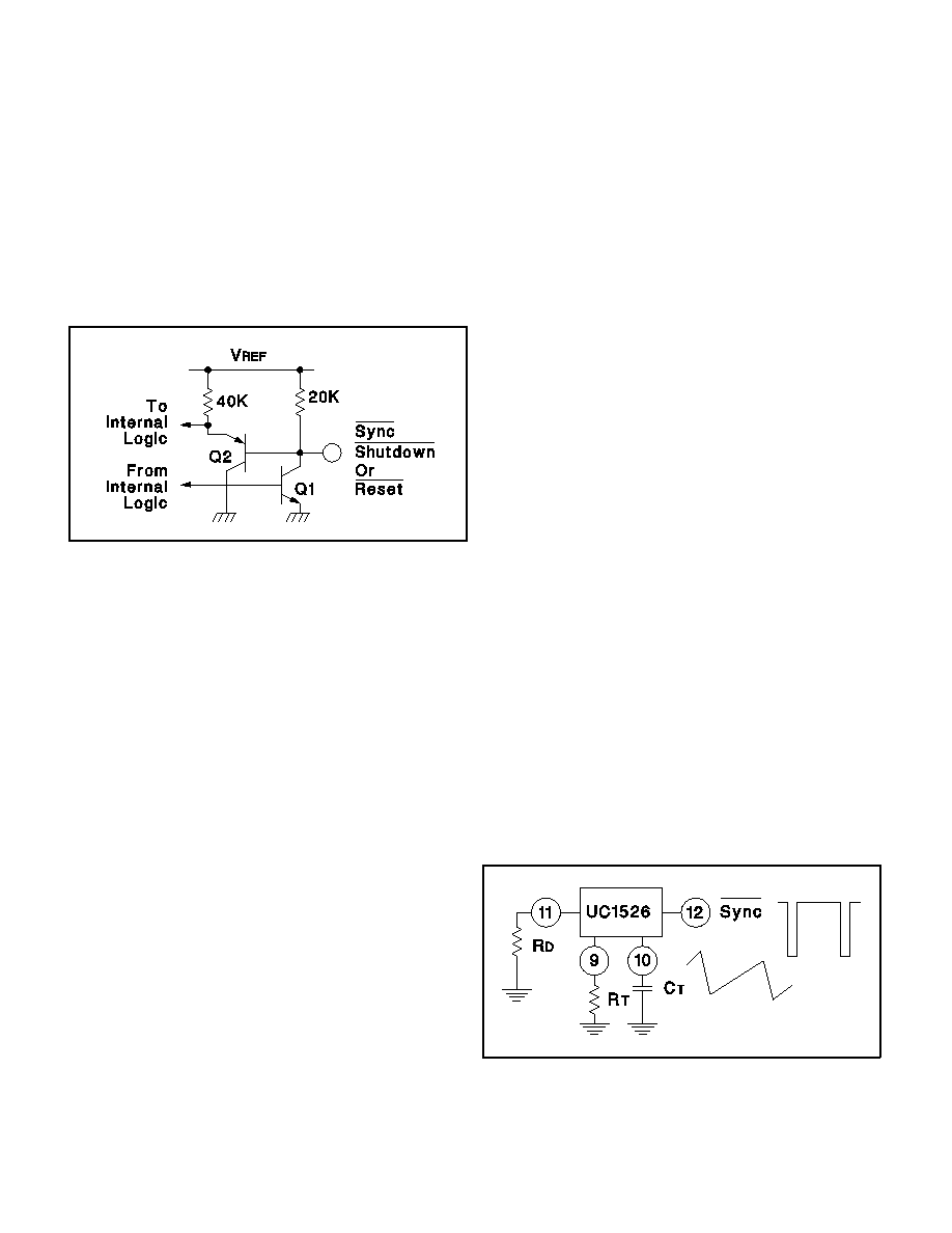
TTL, open-drain CMOS, and open-collector voltage com-
parators; fan-in is equivalent to 1 low-power Schottky
gate. Each port is normally HIGH; the pin is pulled LOW
to activate the particular function. Driving SYNC
______
LOW in-
itiates a discharge cycle in the oscillator. Pulling
SHUTDOWN
____________
LOW immediately inhibits all PWM output
pulses. Holding RESET
_______
LOW discharges the soft-start
capacitor. The logic threshold is +1.1V at +25°C. Noise
immunity can be gained at the expense of fan-out with an
external 2k pull-up resistor to +5V.
Oscillator
The oscillator is programmed for frequency and dead time
with three components: R
T
, C
T
and R
D
. Two waveforms
are generated: a sawtooth waveform at pin 10 for pulse
width modulation, and a logic clock at pin 12. The follow-
ing procedure is recommended for choosing timing val-
ues:
1. With R
D
= 0 (pin 11 shorted to ground) select values
for R
T
and C
T
from Figure 7 to give the desired oscillator
period. Remember that the frequency at each driver out-
put is half the oscillator frequency, and the frequency at
the +V
C
terminal is the same as the oscillator frequency.
2. If more dead time is required, select a large value of
R
D
. At 40kHz dead time increases by 400ns/
.
3. Increasing the dead time will cause the oscillator fre-
quency to decrease slightly. Go back and decrease the
value of R
T
slightly to bring the frequency back to the
nominal design value.
The UC1526 can be synchronized to an external logic
clock by programming the oscillator to free-run at a fre-
quency 10% slower than the sync frequency. A periodic
LOW logic pulse approximately 0.5
µ
s wide at the SYNC
______
pin will then lock the oscillator to the external frequency.
Multiple devices can be synchronized together by pro-
gramming one master unit for the desired frequency and
then sharing its sawtooth and clock waveforms with the
slave units. All C
T
terminals are connected to the C
T
pin
of the master, and all SYNC
______
terminals are likewise con-
nected to the SYNC
______
pin of the master. Slave R
T
termi-
nals are left open or connected to V
REF
. Slave R
D
terminals may be either left open or grounded.
Error Amplifier
The error amplifier is a transconductance design, with an
output impedance of 2M
. Since all voltage gain takes
place at the output pin, the open-loop gain/frequency
characteristics can be controlled with shunt reactance to
ground. When compensated for unity-gain stability with
100pF, the amplifier has an open-loop pole at 800Hz.
The input connections to the error amplifier are deter-
mined by the polarity of the switching supply output volt-
age. For positive supplies, the common-mode voltage is
+5.0V and the feedback connections in Figure 6A are
used. With negative supplies, the common-mode voltage
is ground and the feedback divider is connected between
the negative output and the +5.0V reference voltage, as
shown in Figure 6B.
Output Drivers
The totem-pole output drivers of the UC1526 are de-
signed to source and sink 100mA continuously and
200mA peak. Loads can be driven either from the output
pins 13 and 16, or from the +V
C
, as required.
Since the bottom transistor of the totem-pole is allowed to
saturate, there is a momentary conduction path from the
+V
C
terminal to ground during switching. To limit the re-
sulting current spikes a small resistor in series with pin 14
is always recommended. The resistor value is deter-
mined by the driver supply voltage, and should be chosen
for 200mA peak currents.
UC1526
UC2526
UC3526
Figure 5.
Oscillator Connections and Waveforms
Figure 4.
Digital Control Port Schematic
APPLICATIONS INFORMATION (cont.)
5