Simple Step-Up Voltage Regulator
À
Requires Few External Components
À
NPN Output Switches 3.0A, 65V(max)
À
Extended Input Voltage Range: 3.0V to 40V
À
Current Mode Operation for Improved
Transient Response, Line Regulation, and
Current Limiting
À
Soft Start Function Provides Controlled
Startup
À
52kHz Internal Oscillator
À
Output Switch Protected by Current Limit,
Undervoltage Lockout and Thermal
Shutdown
À
Improved Replacement for LM2577-ADJ
Series
The UC2577-ADJ device provides all the active functions neces-
sary to implement step-up (boost), flyback, and forward converter
switching regulators. Requiring only a few components, these sim-
ple regulators efficiently provide up to 60V as a step-up regulator,
and even higher voltages as a flyback or forward converter regula-
tor.
The UC2577-ADJ features a wide input voltage range of 3.0V to
40V and an adjustable output voltage. An on-chip 3.0A NPN switch
is included with undervoltage lockout, thermal protection circuitry,
and current limiting, as well as soft start mode operation to reduce
current during startup. Other features include a 52kHz fixed fre-
quency on-chip oscillator with no external components and current
mode control for better line and load regulation.
A standard series of inductors and capacitors are available from
several manufacturers optimized for use with these regulators and
are listed in this data sheet.
UC2577-ADJ
3/97
FEATURES
DESCRIPTION
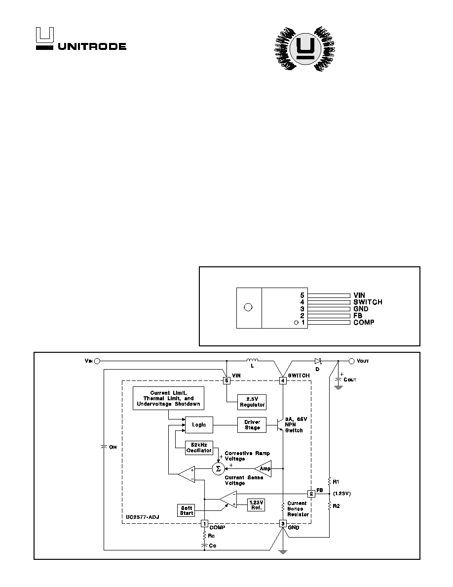
CONNECTION DIAGRAM
BLOCK DIAGRAM
UDG-94034
À
Simple Boost and Flyback Converters
À
SEPIC Topology Permits Input Voltage to
be Higher or Lower than Output Voltage
À
Transformer Coupled Forward Regulators
À
Multiple Output Designs
TYPICAL APPLICATIONS
5-Pin TO-220 (Top View)
T Package
Also available in TO-263 Package (TD).

PARAMETER
TEST CONDITIONS
MIN
TYP
MAX
UNITS
System Parameters
Circuit Figure 1 (Note 3)
Output Voltage
VIN = 5V to 10V, I
LOAD
= 100mA to 800mA
11.40
12.0
12.60
V
T
J
= 25
░
C
11.60
12.40
V
Line Regulation
VIN = 3.0V to 10V, I
LOAD
= 300mA
20
100
mV
T
J
= 25
░
C
50
mV
Load Regulation
VIN = 5V, I
LOAD
= 100mA to 800mA
20
100
mV
T
J
= 25
░
C
50
mV
Efficiency
VIN = 5V, I
LOAD
= 800mA
80
%
Device Parameters
Input Supply Current
V
FB
= 1.5V (Switch Off)
7.5
14
mA
T
J
= 25
░
C
10
mA
I
SWITCH
= 2.0A, V
COMP
= 2.0V (Max Duty Cycle)
45
85
mA
T
J
= 25
░
C
70
mA
Input Supply UVLO
I
SWITCH
= 100mA
2.70
2.95
V
T
J
= 25
░
C
2.85
V
Oscillator Frequency
Measured at SWITCH Pin, I
SWITCH
= 100mA
42
52
62
kHz
T
J
= 25
░
C
48
56
kHz
Reference Voltage
Measured at FB Pin, VIN = 3.0V to 40V, V
COMP
= 1.0V
1.206
1.230
1.254
V
T
J
= 25
░
C
1.214
1.246
V
Reference Voltage Line Regulation
VIN = 3.0V to 40V
0.5
mV
Error Amp Input Bias Current
V
COMP
= 1.0V
100
800
nA
T
J
= 25
░
C
300
nA
Error Amp Transconductance
I
COMP
=
-
30
Á
A to +30
Á
A, V
COMP
= 1.0V
1600
3700
5800
Á
mho
T
J
= 25
░
C
2400
4800
Á
mho
Error Amp Voltage Gain
V
COMP
= 0.8V to 1.6V, R
COMP
= 1.0MW (Note 4)
250
800
V/V
T
J
= 25
░
C
500
V/V
Error Amplifier Output Swing
Upper Limit V
FB
= 1.0V
2.0
2.4
V
T
J
= 25
░
C
2.2
V
Lower Limit V
FB
= 1.5V
0.3
0.55
V
T
J
= 25
░
C
0.40
V
Error Amp Output Current
V
FB
= 1.0V to 1.5V, V
COMP
= 1.0V
▒
90
▒
200
▒
400
Á
A
T
J
= 25
░
C
▒
130
▒
300
Á
A
Soft Start Current
V
FB
= 1.0V, V
COMP
= 0.5V
1.5
5.0
9.5
Á
A
T
J
= 25
░
C
2.5
7.5
Á
A
Maximum Duty Cycle
V
COMP
= 1.5V, I
SWITCH
= 100mA
90
95
%
T
J
= 25
░
C
93
%
Unless otherwise stated, these specifications apply for T
A
=
-
40
░
C
to
+125
░
C, VIN =
5V, V
FB
= V
REF
, I
SWITCH
= 0, and T
A
=T
J
.
ELECTRICAL CHARACTERISTICS
RECOMMENDED OPERATING RANGE
Supply Voltage . . . . . . . . . . . . . . . . . . . . . . . . . . . . . . . . . . . 45V
Output Switch Voltage . . . . . . . . . . . . . . . . . . . . . . . . . . . . . 65V
Output Switch Current (Note 2) . . . . . . . . . . . . . . . . . . . . . 6.0A
Power Dissipation . . . . . . . . . . . . . . . . . . . . . . Internally Limited
Storage Temperature Range . . . . . . . . . . . . .
-
65
░
C to +150
░
C
Lead Temperature (Soldering, 10 sec.) . . . . . . . . . . . . . . 260
░
C
Maximum Junction Temperature . . . . . . . . . . . . . . . . . . . 150
░
C
Minimum ESD Rating (C = 100pF, R = 15k
) . . . . . . . . . . . 2kV
ABSOLUTE MAXIMUM RATINGS (Note 1)
UC2577-ADJ
Supply Voltage . . . . . . . . . . . . . . . . . . . . . . . . 3.0V
VIN
40V
Output Switch Voltage . . . . . . . . . . . . . . . 0V
V
SWITCH
60V
Output Switch Current . . . . . . . . . . . . . . . . . . . . I
SWITCH
3.0A
Junction Temperature Range . . . . . . . . . .
-
40
░
C
T
J
+125
░
C
2

UC2577-ADJ
PARAMETER
TEST CONDITIONS
MIN
TYP
MAX
UNITS
Device Parameters (cont.)
Switch Transconductance
12.5
A/V
Switch Leakage Current
V
SWITCH
= 65V, V
FB
= 1.5V (Switch Off)
10
600
Á
A
T
J
= 25
░
C
300
Á
A
Switch Saturation Voltage
I
SWITCH
= 2.0A, V
COMP
= 2.0V (Max Duty Cycle)
0.5
0.9
V
T
J = 25
░
C
0.7
V
NPN Switch Current Limit
V
COMP
= 2.0V
3.0
4.3
6.0
A
Thermal Resistance
Junction to Ambient
65
░
C/W
Junction to Case
2
░
C/W
COMP Pin Current
V
COMP
= 0
25
50
Á
A
T
J
= 25
░
C
40
Á
A
Unless otherwise stated, these specifications apply for T
A
=
-
40
░
C
to
+125
░
C, VIN =
5V, V
FB
= V
REF
, I
SWITCH
= 0, and T
A
=T
J
.
ELECTRICAL CHARACTERISTICS
Note 1: Absolute Maximum Ratings indicate limits beyond which damage to the device may occur. Operating ratings
indicate conditions during which the device is intended to be functional, but device parameter specifications may not be
guaranteed under these conditions. For guaranteed specifications and test conditions, see the Electrical Characteristics.
Note 2: Output current cannot be internally limited when the UC2577 is used as a step-up regulator. To prevent damage to
the switch, its current must be externally limited to 6.0A. However, output current is internally limited when the UC2577 is
used as a flyback or forward converter regulator.
Note 3. External components such as the diode, inductor, input and output capacitors can affect switching regulator
performance. When the UC2577 is used as shown in the Test Circuit, system performance will be as specified by the
system parameters.
Note 4: A 1.0M
resistor is connected to the compensation pin (which is the error amplifier's output) to ensure accuracy in
measuring A
VOL.
In actual applications, this pin's load resistance should be
10M
, resulting in A
VOL
that is typically twice
the guaranteed minimum limit.
Figure 1. Circuit Used to Specify System Parameters
UDG-94035
L = 415-0930 (AIE)
D = any manufacturer
C
OUT
= Sprague Type 673D
Electrolytic 680
Á
F, 20V
R1 = 48.7k in series with 511
(1%)
R2 = 5.62k (1%)
3

The Block Diagram shows a step-up switching regulator
utilizing the UC2577. The regulator produces an output
voltage higher than the input voltage. The UC2577 turns
its switch on and off at a fixed frequency of 52kHz, thus
storing energy in the inductor (L). When the NPN switch
is on, the inductor current is charged at a rate of VIN/L.
When the switch is off, the voltage at the SWITCH termi-
nal of the inductor rises above VIN, discharging the
stored current through the output diode (D) into the out-
put capacitor (C
OUT
) at a rate of (V
OUT
- VIN)/L. The en-
ergy stored in the inductor is thus transferred to the
output.
The output voltage is controlled by the amount of energy
transferred, which is controlled by modulating the peak
inductor current. This modulation is accomplished by
feeding a portion of the output voltage to an error ampli-
fier which amplifies the difference between the feedback
voltage and an internal 1.23V precision reference volt-
age. The output of the error amplifier is then compared to
a voltage proportional to the switch current, or the induc-
tor current, during the switch on time. A comparator ter-
minates the switch on time when the two voltages are
equal and thus controls the peak switch current to main-
tain a constant output voltage. Figure 2 shows voltage
and current waveforms for the circuit. Formulas for calcu-
lation are shown in Figure 3.
STEP-UP REGULATOR DESIGN PROCEDURE
Refer to the Block Diagram
Given:
V
INmin
= Minimum input supply voltage
V
OUT
= Regulated output voltage
UC2577-ADJ
Step-up (Boost) Regulator
Duty Cycle
D
V
OUT
+
V
F
-
V
IN
V
OUT
+
V
F
-
V
SAT
V
OUT
-
V
IN
V
OUT
Avg. Inductor
Current
I
IND(AVG)
I
LOAD
1
-
D
Inductor
Current Ripple
I
IND
V
IN
-
V
SAT
L
À
D
52,000
Peak Inductor
Current
I
IND(PK)
I
LOAD
1
-
D
+
I
IND
2
Peak Switch
Current
I
SW(PK)
I
LOAD
1
-
D
+
I
IND
2
Switch Voltage
when Off
V
SW(OFF)
V
OUT
+ V
F
Diode Reverse
Voltage
V
R
V
OUT
- V
SAT
Avg. Diode
Current
I
D(AVG)
I
LOAD
Peak Diode
Current
I
D(PK)
I
LOAD
1
-
D
+
I
IND
2
.
Power
Dissipation
P
D
0.25
I
LOAD
1
-
D
2
D
+
I
LOAD
À
D
À
V
IN
50
(
1
-
D
)
V
F
= Forward Biased Diode Voltage, I
LOAD
= Output Load
Figure 2. Step-up Regulator Waveforms
First, determine if the UC2577 can provide these values
of V
OUT
and I
LOADmax
when operating with the minimum
value of V
IN
. The upper limits for V
OUT
and I
LOADmax
are
given by the following equations.
V
OUT
60V and
V
OUT
10
À
V
INmin
I
LOADmax
2.1A
À
V
INmin
V
OUT
These limits must be greater than or equal to the values
specified in this application.
1. Output Voltage Section
Resistors R1 and R2 are used to select the desired out-
put voltage. These resistors form a voltage divider and
present a portion of the output voltage to the error ampli-
fier which compares it to an internal 1.23V reference. Se-
lect R1 and R2 such that:
R1
R2
=
V
OUT
1.23V
-
1
Figure 3. Step-up Regulator Formulas
APPLICATIONS INFORMATION
4
2. Inductor Selection (L)
A. Preliminary Calculations
To select the inductor, the calculation of the following
three parameters is necessary:
Dmax, the maximum switch duty cycle (0
D
0.9):
D
max
=
V
OUT
+
V
F
-
V
INmin
V
OUT
+
V
F
-
0.6V
where typically V
F
= 0.5V for Schottky diodes and V
F
=
0.8V for fast recovery diodes.
E
À
T, the product of volts
À
time that charges the induc-
tor:
E
À
T
=
D
max
À
(
V
INmin
-
0.6V
)
10
6
52,000Hz
(
V
À
Á
s
)
I
IND, DC
, the average inductor current under full load:
I
IND,
DC
=
1.05
À
I
LOADmax
1
-
D
max
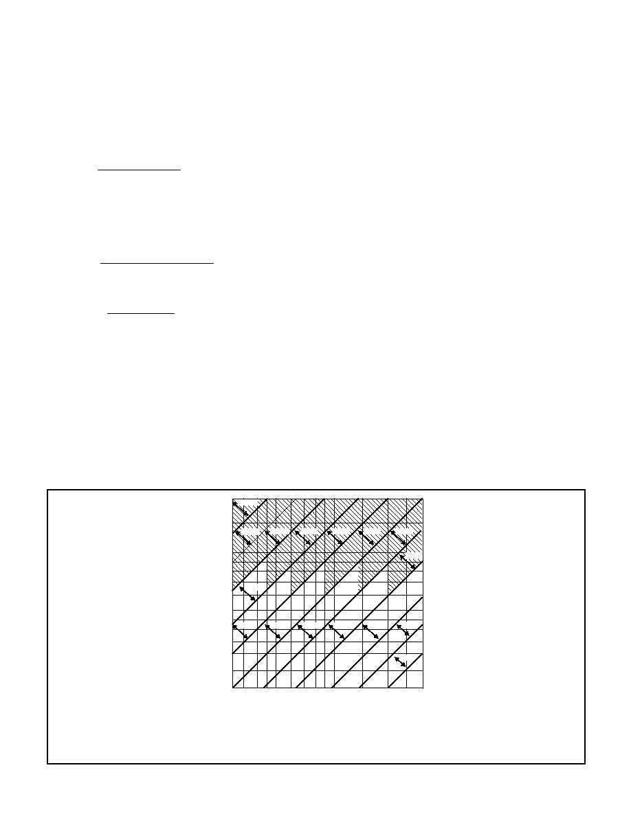
B. Identify Inductor Value:
1. From Figure 4, identify the inductor code for the region
indicated by the intersection of E
À
T and I
IND, DC
. This
code gives the inductor value in microhenries. The L or H
prefix signifies whether the inductor is rated for a maxi-
mum E
À
T of 90V
Á
s (L) or 250V
Á
s (H).
2. If D < 0.85, go to step C. If D
0.85, calculate the
minimum inductance needed to ensure the switching
regulator's stability:
0.3
0.4 0.45
0.35
0.5 0.6 0.7 0.8 0.9 1.0
1.5
2.0
2.5
3.0
20
30
35
25
40
45
50
60
70
80
90
100
200
150
L47
L68
L100
L150
L220
L330
H2200
L680
H1500
H1000
H680
H470
H330
H220
H150
L470
EÀT (VÀ
Á
s)
I
IND, DC
(A)
Figure 4. Inductor Selection Graph
If L
min
is smaller than the inductor values found in step
B1, go on to step C. Otherwise, the inductor value found
in step B1 is too low; an appropriate inductor code
should be obtained from the graph as follows:
1.
Find the lowest value inductor that is greater than
L
min
.
2.
Find where E
À
T intersects this inductor value to
determine if it has an L or H prefix. If E
À
T intersects
both the L and H regions, select the inductor with an
H prefix.
C.
Inductor Selection
Select an inductor from the table of Figure 5 which cross
references the inductor codes to the part numbers of the
three different manufacturers. The inductors listed in this
table have the following characteristics:
AIE
(ferrite, pot-core inductors): Benefits of this type
are low etectromagnetic interference (EMI), small
physical size, and very low power dissipation (core
loss).
Pulse
(powdered iron, toroid core inductors): Bene-
fits are low EMI and ability to withstand E
À
T and
peak current above rated value better than ferrite
cores.
Renco
(ferrite, bobbin-core inductors): Benefits are
low cost and best ability to withstand E
À
T and peak
current above rated value. Be aware that these in-
ductors generate more EMI than the other types, and
this may interfere with signals sensitive to noise.
UC2577-ADJ
Note: This chart assumes that the inductor ripple current inductor is approximately 20% to 30% of the average inductor current
(when the regulator is under full load). Greater ripple current causes higher peak switch currents and greater output ripple volt-
age. Lower ripple current is achieved with larger value inductors. The factor of 20% to 30% is chosen as a convenient balance
between the two extremes.
APPLICATIONS INFORMATION (cont.)
5