TSL245
INFRARED LIGHT-TO-FREQUENCY CONVERTER
SOES018 ¡ MAY 1995
1
POST OFFICE BOX 655303
À
DALLAS, TEXAS 75265
D
High-Resolution Conversion of Light
Intensity to Frequency With No External
Components
D
Direct Interface With a Microcontroller
D
Compact Three-Leaded Plastic Package
D
Single-Supply Operation Down to 2.7 V
D
Nonlinearity Error Typically 0.2% at 100 kHz
D
Advanced LinCMOS
TM
Technology
D
Integral Visible-Light Cutoff Filter
description
The TSL245 infrared light-to-frequency converter combines a silicon photodiode and a current-to-frequency
converter on a single monolithic CMOS integrated circuit. The output is a square wave (50% duty cycle) with
frequency directly proportional to light intensity. Because the output is TTL compatible, it allows direct interface
to a microcontroller or other logic circuitry. The device responds over the infrared light range of 800 nm to
1100 nm. The TSL245 is characterized for operation over the temperature range of ¡ 25
░
C to 70
░
C.
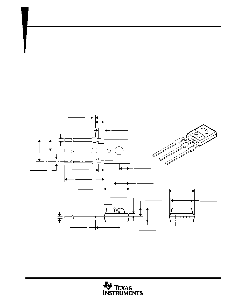
The TSL245 is offered in a black, infrared-transmissive package (see Figure 1). The photodiode area is
1.36 mm
2
(0.0029 in
2
).
2,25 (0.089)
1,75 (0.069)
0,75 (0.030)
0,65 (0.026)
0,635 (0.025)
0,4 (0.016)
2,0 (0.079) T.P.
4,0 (0.157) T.P.
1
2
3
15,7 (0.619)
13,2 (0.520)
0,86 (0.034)
0,46 (0.018)
2,05 (0.081)
1,55 (0.061)
3,05 (0.120)
2,55 (0.100)
4,8 (0.189)
4,4 (0.173)
0,75 (0.030) R
0,85 (0.033)
0,35 (0.014)
2,74 (0.108)
2,34 (0.092)
5,05 (0.199)
4,55 (0.179)
4,85 (0.191)
4,35 (0.171)
4,35 (0.171)
3,85 (0.152)
Pin 1
GND
Pin 2
VDD
Pin 3
OUT
1
2
3
0,51 (0.02)
0,385 (0.015)
1,25 (0.049)
0,75 (0.030)
1,75 (0.069)
1,25 (0.049)
0,65 (0.026)
0,55 (0.022)
True position when unit is installed.
NOTE A: All linear dimensions are in millimeters and parenthetically in inches.
Figure 1. TSL245 Packaging Configuration
Copyright
®
1995, Texas Instruments Incorporated
PRODUCTION DATA information is current as of publication date.
Products conform to specifications per the terms of Texas Instruments
standard warranty. Production processing does not necessarily include
testing of all parameters.
Advanced LinCMOS is a trademark of Texas Instruments Incorporated.

TSL245
INFRARED LIGHT-TO-FREQUENCY CONVERTER
SOES018 ¡ MAY 1995
2
POST OFFICE BOX 655303
À
DALLAS, TEXAS 75265
functional block diagram
Light
Current-to-Frequency
Converter
Photodiode
Output
absolute maximum ratings over operating free-air temperature range (unless otherwise noted)
Supply voltage, V
DD
(see Note 1)
6.5 V
. . . . . . . . . . . . . . . . . . . . . . . . . . . . . . . . . . . . . . . . . . . . . . . . . . . . . . . . . . .
Operating free-air temperature range, T
A
¡ 25
░
C to 70
░
C
. . . . . . . . . . . . . . . . . . . . . . . . . . . . . . . . . . . . . . . . . . . .
Storage temperature range, T
stg
¡ 25
░
C to 85
░
C
. . . . . . . . . . . . . . . . . . . . . . . . . . . . . . . . . . . . . . . . . . . . . . . . . . . .
Lead temperature 1,6 mm (1/16 inch) from case for 10 seconds
260
░
C
. . . . . . . . . . . . . . . . . . . . . . . . . . . . . . .
Stresses beyond those listed under "absolute maximum ratings" may cause permanent damage to the device. These are stress ratings only, and
functional operation of the device at these or any other conditions beyond those indicated under "recommended operating conditions" is not
implied. Exposure to absolute-maximum-rated conditions for extended periods may affect device reliability.
NOTE 1: All voltage values are with respect to GND.
recommended operating conditions
MIN
NOM
MAX
UNIT
Supply voltage, VDD
2.7
5
6
V
Operating free-air temperature range, TA
¡ 25
70
░
C
electrical characteristics at V
DD
= 5 V, T
A
= 25
░
C (unless otherwise noted)
PARAMETER
TEST CONDITIONS
MIN
TYP
MAX
UNIT
VOH
High-level output voltage
IOH = ¡ 4 mA
4
4.3
V
VOL
Low-level output voltage
IOL = 4 mA
0.17
0.26
V
IDD
Supply current
2
3
mA
Full-scale frequency
500
kHz
kSVS
Supply-voltage sensitivity
VDD = 5 V
▒
10%
0.5
%/ V
Full-scale frequency is the maximum operating frequency of the device without saturation.
operating characteristics at V
DD
= 5 V, T
A
= 25
░
C
PARAMETER
TEST CONDITIONS
MIN
TYP
MAX
UNIT
fO
Output frequency
Ee = 920
Á
W/cm2,
p = 940 nm
200
250
300
kHz
fO
Output frequency
Ee = 0
0.25
10
Hz
Nonlinearity º
fO = 0 kHz to 10 kHz
▒
0.1%
%F.S.
Nonlinearity º
fO = 0 kHz to 100 kHz
▒
0.2%
%F.S.
Step response to full-scale step input
1 pulse of new
frequency plus 1
Á
s
Full-scale frequency is the maximum operating frequency of the device without saturation.
º Nonlinearity is defined as the deviation of fO from a straight line between zero and full scale, expressed as a percent of full scale.
TSL245
INFRARED LIGHT-TO-FREQUENCY CONVERTER
SOES018 ¡ MAY 1995
3
POST OFFICE BOX 655303
À
DALLAS, TEXAS 75265
TYPICAL CHARACTERISTICS
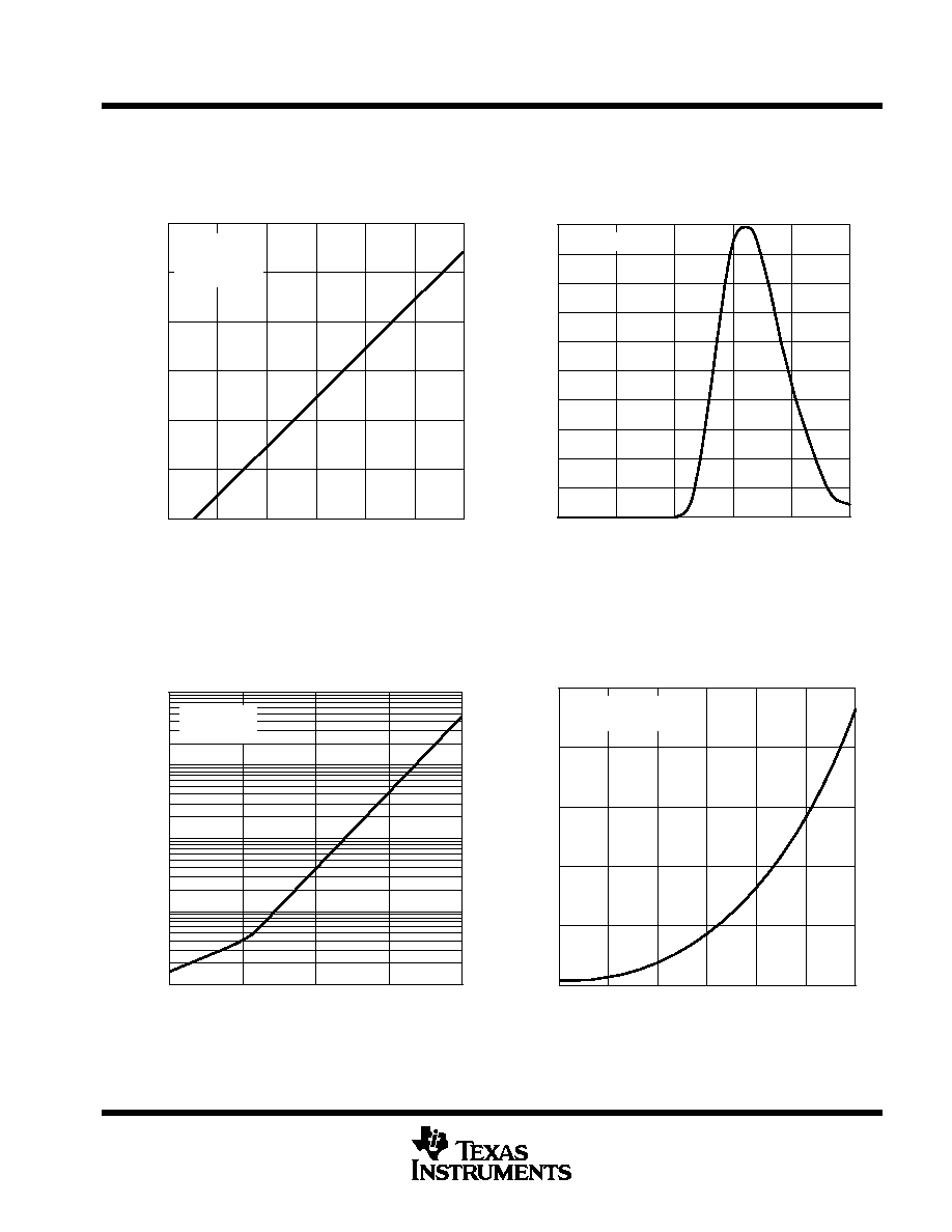
Figure 2
1
0.1
0.01
0.001
0.001
0.01
0.1
1
10
¡ Output Frequency ¡ kHz
10
100
OUTPUT FREQUENCY
vs
IRRADIANCE
10 0
1 k
Ee ¡ Irradiance ¡
Á
W/cm2
f O
VDD = 5 V
p = 940 nm
TA = 25
░
C
1000
Figure 3
PHOTODIODE SPECTRAL RESPONSIVITY
¡ Wavelength ¡ nm
Normalized Responsivity
0.5
0.4
0.2
0.1
0
0.9
0.3
600
700
800
900
0.7
0.6
0.8
1
1000
1100
TA = 25
░
C
0.1
0.01
¡ 25
0
25
50
1
DARK FREQUENCY
vs
TEMPERATURE
10
75
VDD = 5 V
Ee = 0
100
¡ Dark Frequency ¡ Hz
f O(dark)
TA ¡ Temperature ¡
░
C
Figure 4
¡ Wavelength of Incident Light ¡ nm
T
emperature Coefficient of Output Frequency ¡ ppm/
░
C
TEMPERATURE COEFFICIENT
OF OUTPUT FREQUENCY
vs
WAVELENGTH OF INCIDENT LIGHT
4000
0
700
800
900
1000
6000
8000
2000
VDD = 5 V
TA = 25
░
C to 70
░
C
10000
750
850
950
Figure 5
TSL245
INFRARED LIGHT-TO-FREQUENCY CONVERTER
SOES018 ¡ MAY 1995
4
POST OFFICE BOX 655303
À
DALLAS, TEXAS 75265
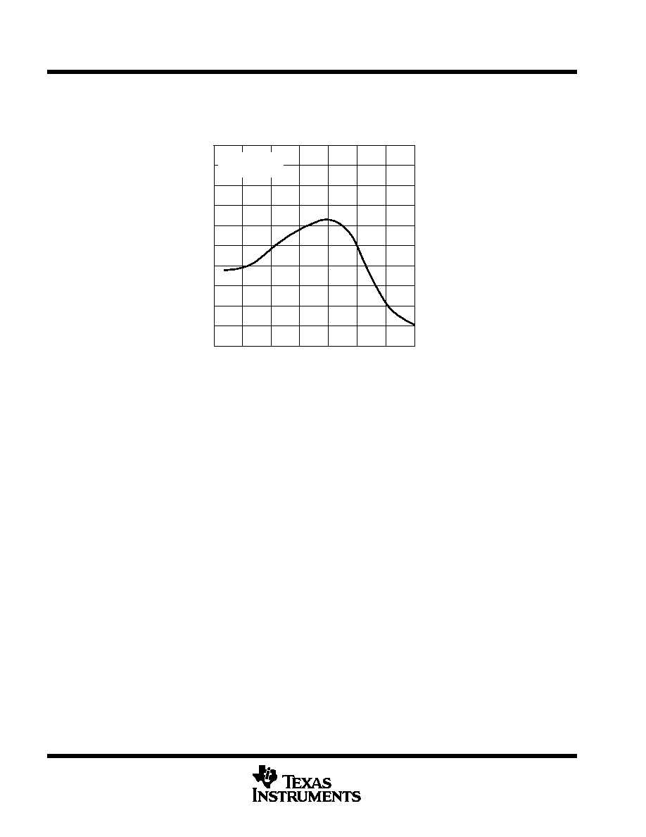
TYPICAL CHARACTERISTICS
0.998
0.997
0.996
0.995
2.5
3
3.5
4
4.5
Normalized Output Frequency
0.999
1
OUTPUT FREQUENCY
vs
SUPPLY VOLTAGE
5
5.5
VDD ¡ Supply Voltage ¡ V
TA = 25
░
C
fO = 500 kHz
1.001
6
1.002
1.003
1.004
1.005
Figure 6
TSL245
INFRARED LIGHT-TO-FREQUENCY CONVERTER
SOES018 ¡ MAY 1995
5
POST OFFICE BOX 655303
À
DALLAS, TEXAS 75265
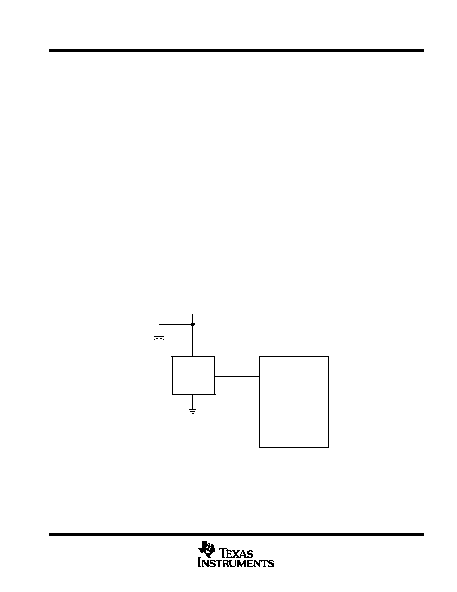
APPLICATION INFORMATION
power-supply considerations
For optimum device performance, power-supply lines should be decoupled by a 0.01-
Á
F to 0.1-
Á
F capacitor
with short leads (see Figure 7).
output interface
The output of the device is designed to drive a standard TTL or CMOS logic input over short distances. If lines
greater than 12 inches are used on the output, a buffer or line driver is recommended.
measuring the frequency
The choice of interface and measurement techniques depends on the desired resolution and data-acquisition
rate. For maximum data-acquisition rate, period-measurement techniques should be used.
Period measurement requires using a fast reference clock with available resolution directly related to reference
clock rate. The technique measures rapidly varying light levels or provides a fast measurement of a constant
light source.
Maximum resolution and accuracy can be obtained using frequency-measurement, pulse-accumulation, or
integration techniques. Frequency measurements provide the added benefit of averaging random- or
high-frequency variations (jitter) resulting from noise in the light signal. Resolution is limited primarily by
available counter registers and allowable measurement time. Frequency measurement is well suited for slowly
varying or constant light levels and for reading average light levels over short periods of time. Integration, the
accumulation of pulses over a very long period of time, can be used to measure exposure ¡ the amount of light
present in an area over a given time period.
TSL245
Timer / Port
MCU
0.1
Á
F
VDD
2
3
1
Figure 7. Typical TSL245 Interface to a Microcontroller