TSL235
LIGHT-TO-FREQUENCY CONVERTER
SOES012 SEPTEMBER 1994
Copyright
©
1994, Texas Instruments Incorporated
1
POST OFFICE BOX 655303
·
DALLAS, TEXAS 75265
·
High-Resolution Conversion of Light
Intensity to Frequency With No External
Components
·
Communicates Directly With a
Microcontroller
·
Compact Three-Leaded Clear-Plastic
Package
·
Single-Supply Operation Down to 2.7 V
·
Nonlinearity Error Typically 0.2% at 100 kHz
·
Stable 100 ppm/
°
C Temperature Coefficient
·
Advanced LinCMOS
TM
Technology
description
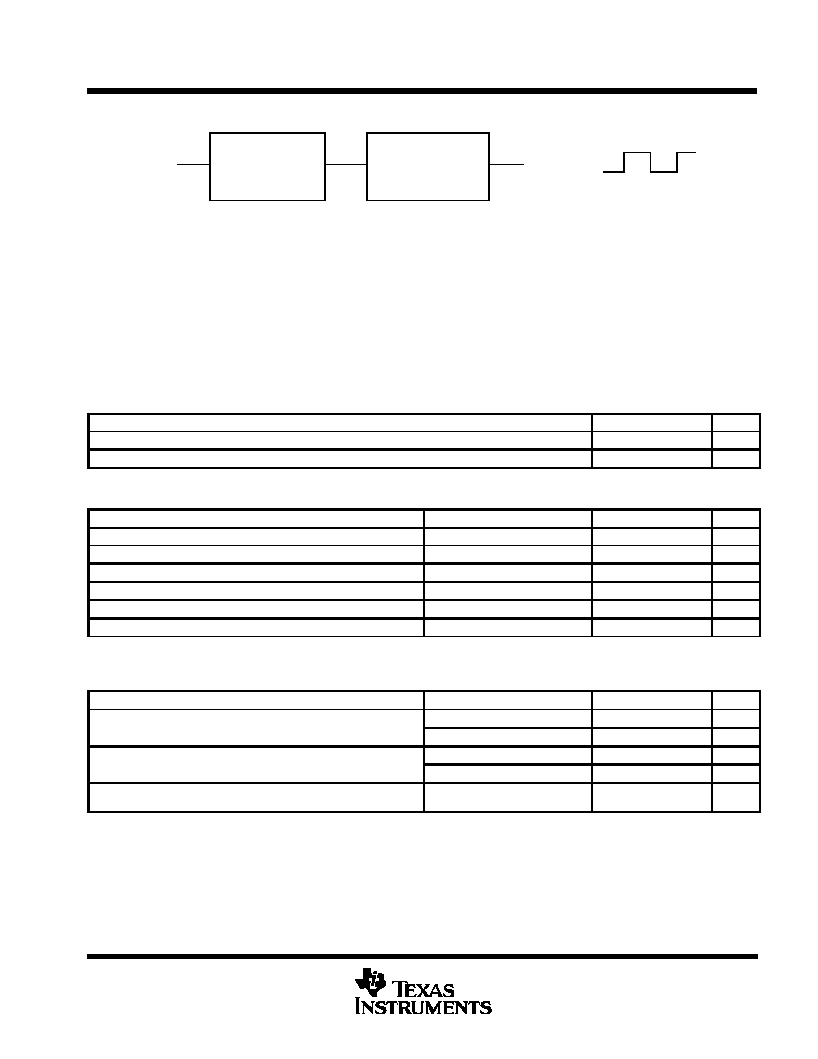
The TSL235 light-to-frequency converter combines a silicon photodiode and a current-to-frequency converter
on a single monolithic CMOS integrated circuit. The output is a square wave (50% duty cycle) with frequency
directly proportional to light intensity. Because it is TTL compatible, the output allows direct interface to a
microcontroller or other logic circuitry. The device has been temperature compensated for the ultraviolet-
to-visible light range of 300 nm to 700 nm and responds over the light range of 300 nm to 1100 nm. The TSL235
is characterized for operation over the temperature range of 25
°
C to 70
°
C.
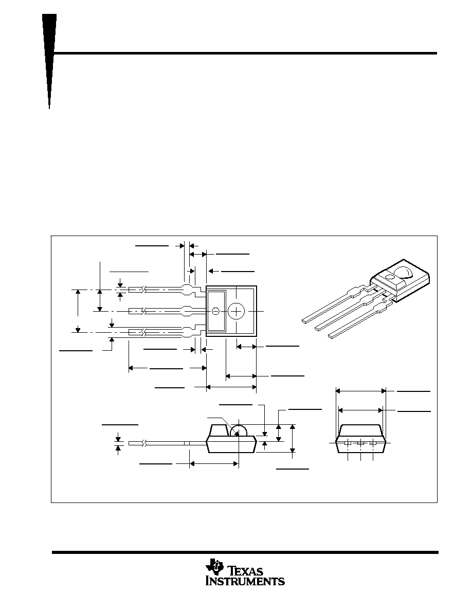
mechanical data
The TSL235 is offered in a clear-plastic three-leaded package. The photodiode area is 1.36 mm
2
(0.0029 in
2
).
2,25 (0.089)
1,75 (0.069)
0,75 (0.030)
0,65 (0.026)
0,635 (0.025)
0,4 (0.016)
2,0 (0.079) T.P.
4,0 (0.157) T.P.
1
2
3
15,7 (0.619)
13,2 (0.520)
0,86 (0.034)
0,46 (0.018)
2,05 (0.081)
1,55 (0.061)
3,05 (0.120)
2,55 (0.100)
4,8 (0.189)
4,4 (0.173)
0,75 (0.030) R
0,85 (0.033)
0,35 (0.014)
2,74 (0.108)
2,34 (0.092)
5,05 (0.199)
4,55 (0.179)
4,85 (0.191)
4,35 (0.171)
4,35 (0.171)
3,85 (0.152)
Pin 1
GND
Pin 2
VDD
Pin 3
OUT
ALL LINEAR DIMENSIONS ARE IN MILLIMETERS AND PARENTHETICALLY IN INCHES
1
2
3
0,51 (0.02)
0,385 (0.015)
1,25 (0.049)
0,75 (0.029)
1,75 (0.069)
1,25 (0.049)
0,65 (0.026)
0,55 (0.022)
True position when unit is installed.
Advanced LinCMOS is a trademark of Texas Instruments Incorporated.
PRODUCTION DATA information is current as of publication date.
Products conform to specifications per the terms of Texas Instruments
standard warranty. Production processing does not necessarily include
testing of all parameters.
TSL235
LIGHT-TO-FREQUENCY CONVERTER
SOES012 SEPTEMBER 1994
2
POST OFFICE BOX 655303
·
DALLAS, TEXAS 75265
functional block diagram
Light
Current-to-Frequency
Converter
Photodiode
Output
absolute maximum ratings over operating free-air temperature range (unless otherwise noted)
Supply voltage, V
DD
(see Note 1)
6.5 V
. . . . . . . . . . . . . . . . . . . . . . . . . . . . . . . . . . . . . . . . . . . . . . . . . . . . . . . . . . .
Operating free-air temperature range, T
A
25
°
C to 70
°
C
. . . . . . . . . . . . . . . . . . . . . . . . . . . . . . . . . . . . . . . . . . . .
Storage temperature range
25
°
C to 85
°
C
. . . . . . . . . . . . . . . . . . . . . . . . . . . . . . . . . . . . . . . . . . . . . . . . . . . . . . . . .
Lead temperature 1,6 mm (1/16 inch) from case for 10 seconds
260
°
C
. . . . . . . . . . . . . . . . . . . . . . . . . . . . . . .
Stresses beyond those listed under "absolute maximum ratings" may cause permanent damage to the device. These are stress ratings only, and
functional operation of the device at these or any other conditions beyond those indicated under "recommended operating conditions" is not
implied. Exposure to absolute-maximum-rated conditions for extended periods may affect device reliability.
NOTE 1: All voltage values are with respect to GND.
recommended operating conditions
MIN
NOM
MAX
UNIT
Supply voltage, VDD
2.7
5
6
V
Operating free-air temperature range, TA
25
70
°
C
electrical characteristics at V
DD
= 5 V, T
A
= 25
°
C (unless otherwise noted)
PARAMETER
TEST CONDITIONS
MIN
TYP
MAX
UNIT
VOH
High-level output voltage
IOH = 4 mA
4
4.3
V
VOL
Low-level output voltage
IOL = 4 mA
0.17
0.26
V
IDD
Supply current
2
3
mA
Full-scale frequency
500
kHz
Temperature coefficient of output frequency
700 nm, 25
°
C
TA
70
°
C
±
100
ppm/
°
C
kSVS
Supply-voltage sensitivity
VDD = 5 V
±
10%
0.5
%/ V
Full-scale frequency is the maximum operating frequency of the device without saturation.
operating characteristics at V
DD
= 5 V, T
A
= 25
°
C
PARAMETER
TEST CONDITIONS
MIN
TYP
MAX
UNIT
fO
Output frequency
Ee = 375
µ
W/cm2,
p = 670 nm
200
250
300
kHz
fO
Output frequency
Ee = 0
0.25
10
Hz
Nonlinearity §
fO = 0 kHz to 10 kHz
±
0.1%
%F.S.
Nonlinearity §
fO = 0 kHz to 100 kHz
±
0.2%
%F.S.
Step response to full-scale step input
1 pulse of new
frequency plus 1
µ
s
Full-scale frequency is the maximum operating frequency of the device without saturation.
§ Nonlinearity is defined as the deviation of fO from a straight line between zero and full scale, expressed as a percent of full scale.

TSL235
LIGHT-TO-FREQUENCY CONVERTER
SOES012 SEPTEMBER 1994
3
POST OFFICE BOX 655303
·
DALLAS, TEXAS 75265
TYPICAL CHARACTERISTICS
1
0.1
0.01
0.001
0.001
0.01
0.1
1
10
Output Frequency kHz
10
100
OUTPUT FREQUENCY
vs
IRRADIANCE
10 0
1 k
Ee Irradiance
µ
W/cm2
f O
VDD = 5 V
p = 670 nm
TA = 25
°
C
1000
0.4
0
300
500
700
900
0.6
0.8
PHOTODIODE SPECTRAL RESPONSIVITY
0.2
Wavelength nm
Normalized Responsivity
TA = 25
°
C
1
1100
400
600
800
1000
Figure 1
Figure 2
0.1
0.01
25
0
25
50
1
DARK FREQUENCY
vs
TEMPERATURE
10
75
VDD = 5 V
Ee = 0
100
Dark Frequency Hz
f O(dark)
TA Temperature
°
C
4000
0
300
500
700
900
6000
8000
2000
Wavelength of Incident Light nm
T
emperature Coefficient of Output Frequency ppm/
VDD = 5 V
TA = 25
°
C to 70
°
C
10000
400
600
800
1000
°
C
TEMPERATURE COEFFICIENT
OF OUTPUT FREQUENCY
vs
WAVELENGTH OF INCIDENT LIGHT
Figure 3
Figure 4

TSL235
LIGHT-TO-FREQUENCY CONVERTER
SOES012 SEPTEMBER 1994
4
POST OFFICE BOX 655303
·
DALLAS, TEXAS 75265
TYPICAL CHARACTERISTICS
0.998
0.997
0.996
0.995
2.5
3
3.5
4
4.5
Normalized Output Frequency
0.999
1
OUTPUT FREQUENCY
vs
SUPPLY VOLTAGE
5
5.5
VDD Supply Voltage V
TA = 25
°
C
fO = 500 kHz
1.001
6
1.002
1.003
1.004
1.005
Figure 5
TSL235
LIGHT-TO-FREQUENCY CONVERTER
SOES012 SEPTEMBER 1994
5
POST OFFICE BOX 655303
·
DALLAS, TEXAS 75265
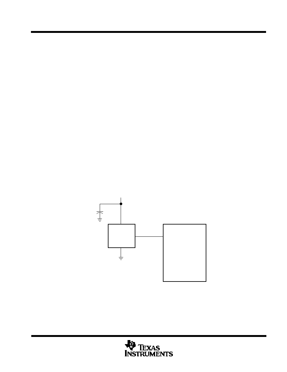
APPLICATION INFORMATION
power-supply considerations
For optimum device performance, power-supply lines should be decoupled by a 0.01-
µ
F to 0.1-
µ
F capacitor with
short leads (see Figure 6).
output interface
The output of the device is designed to drive a standard TTL or CMOS logic input over short distances. If lines
greater than 12 inches are used on the output, a buffer or line driver is recommended.
measuring the frequency
The choice of interface and measurement technique depends on the desired resolution and data-acquisition
rate. For maximum data-acquisition rate, period-measurement techniques are used.
Period measurement requires the use of a fast reference clock with available resolution directly related to
reference-clock rate. The technique is employed to measure rapidly varying light levels or to make a fast
measurement of a constant light source.
Maximum resolution and accuracy may be obtained using frequency-measurement, pulse-accumulation, or
integration techniques. Frequency measurements provide the added benefit of averaging out random- or
high-frequency variations (jitter) resulting from noise in the light signal. Resolution is limited mainly by available
counter registers and allowable measurement time. Frequency measurement is well suited for slowly varying
or constant light levels and for reading average light levels over short periods of time. Integration, the
accumulation of pulses over a very long period of time, can be used to measure exposure the amount of light
present in an area over a given time period.
TSL235
Timer / Port
MCU
0.1
µ
F
VDD
2
3
1
Figure 6. Typical TSL235 Interface to a Microcontroller

IMPORTANT NOTICE
Texas Instruments and its subsidiaries (TI) reserve the right to make changes to their products or to discontinue
any product or service without notice, and advise customers to obtain the latest version of relevant information
to verify, before placing orders, that information being relied on is current and complete. All products are sold
subject to the terms and conditions of sale supplied at the time of order acknowledgement, including those
pertaining to warranty, patent infringement, and limitation of liability.
TI warrants performance of its semiconductor products to the specifications applicable at the time of sale in
accordance with TI's standard warranty. Testing and other quality control techniques are utilized to the extent
TI deems necessary to support this warranty. Specific testing of all parameters of each device is not necessarily
performed, except those mandated by government requirements.
CERTAIN APPLICATIONS USING SEMICONDUCTOR PRODUCTS MAY INVOLVE POTENTIAL RISKS OF
DEATH, PERSONAL INJURY, OR SEVERE PROPERTY OR ENVIRONMENTAL DAMAGE ("CRITICAL
APPLICATIONS"). TI SEMICONDUCTOR PRODUCTS ARE NOT DESIGNED, AUTHORIZED, OR
WARRANTED TO BE SUITABLE FOR USE IN LIFE-SUPPORT DEVICES OR SYSTEMS OR OTHER
CRITICAL APPLICATIONS. INCLUSION OF TI PRODUCTS IN SUCH APPLICATIONS IS UNDERSTOOD TO
BE FULLY AT THE CUSTOMER'S RISK.
In order to minimize risks associated with the customer's applications, adequate design and operating
safeguards must be provided by the customer to minimize inherent or procedural hazards.
TI assumes no liability for applications assistance or customer product design. TI does not warrant or represent
that any license, either express or implied, is granted under any patent right, copyright, mask work right, or other
intellectual property right of TI covering or relating to any combination, machine, or process in which such
semiconductor products or services might be or are used. TI's publication of information regarding any third
party's products or services does not constitute TI's approval, warranty or endorsement thereof.
Copyright
©
1998, Texas Instruments Incorporated