
TRF8010
900-MHz RF TRANSMIT DRIVER
SLWS031B ş JULY 1996ş REVISED MAY 1997
1
POST OFFICE BOX 655303
Ě
DALLAS, TEXAS 75265
D
Operates from 3.6-V and 4.8-V Power
Supplies for AMPS/NADC and GSM
Applications Respectively
D
Unconditionally Stable
D
Wide UHF Frequency Range
800 MHz to 1000 MHz
D
21 dBm and 23 dBm Typical Output Power
in AMPS/NADC and GSM Applications
Respectively
D
Linear Ramp Control
D
Transmit Enable/Disable Control
D
Advanced BiCMOS Processing Technology
for Low-Power Consumption, High
Efficiency, and Highly Linear Operation
D
Minimum of External Components
Required for Operation
D
Surface-Mount Thermally Enhanced
Package for Extremely Small Circuit
Footprint
description
The TRF8010 is an RF transmit driver amplifier for 900-MHz digital, analog, and dual-mode communication
applications. It consists of a two-stage amplifier and a linear ramp controller for burst control in TDMA (time
division multiple access) applications. Very few external components are required for operation.
The TRF8010 amplifies the RF signal from the preceding modulator and upconverter stages in an RF section
of a transmitter to a level that is sufficient to drive a final RF power output device. The output impedance of
RFOUT is approximately 50
.
But, since RFOUT is connected to an open-collector output device, minimal
external matching is required.
The device is enabled when the TXEN input is held high. A power control signal applied to the VPC input can
ramp the RF output power up or down to meet ramp and spurious emission specifications in TDMA systems.
The power control signal causes a linear change in output power as the voltage applied to VPC varies between
0 V and 3 V. With the RF input power applied to RFIN at 0 dBm and TXEN high, adjusting VPC from 0 V to
3 V increases the output power from a typical value of ş54 dBm at VPC = 0 V to the output power appropriate
for the application:
D
21 dBm typical for AMPS/NADC (Advanced Mobile Phone Service/North American Digital Cellular)
operation
D
23 dBm typical for GSM (Global System for Mobile Communications) operation
Forward isolation with the RF input power applied to RFIN at 0 dBm, VPC = 0 V, and TXEN high is typically
greater than 50 dB.
These devices have limited built-in ESD protection. The leads should be shorted together or the device placed in conductive foam
during storage or handling to prevent electrostatic damage to the MOS gates.
Please be aware that an important notice concerning availability, standard warranty, and use in critical applications of
Texas Instruments semiconductor products and disclaimers thereto appears at the end of this data sheet.
1
2
3
4
5
6
7
8
9
10
20
19
18
17
16
15
14
13
12
11
GND
GND
RFIN
GND
NC
VPC
GND
NC
V
BB
GND
GND
GND
RFOUT
GND
GND
TXEN
GND
V
CC
V
CC
GND
PWP PACKAGE
(TOP VIEW)
NC ş No internal connection
PRODUCTION DATA information is current as of publication date.
Products conform to specifications per the terms of Texas Instruments
standard warranty. Production processing does not necessarily include
testing of all parameters.
Copyright
ę
1997, Texas Instruments Incorporated
TRF8010
900-MHz RF TRANSMIT DRIVER
SLWS031B ş JULY 1996ş REVISED MAY 1997
2
POST OFFICE BOX 655303
Ě
DALLAS, TEXAS 75265
description (continued)
The TRF8010 is available in a small, surface-mount, thermally enhanced TSSOP 20-pin PWP (PowerPAD
TM
)
package and is characterized for operation from ş 40
░
C to 85
░
C. The PWP package has a solderable pad that
can improve the package thermal performance by bonding the pad to an external thermal plane. The pad also
acts as a low-inductance electrical path to ground and, for the TRF8010, must be electrically connected to the
PCB ground plane as a continuation of the regular package terminals that are designated GND.
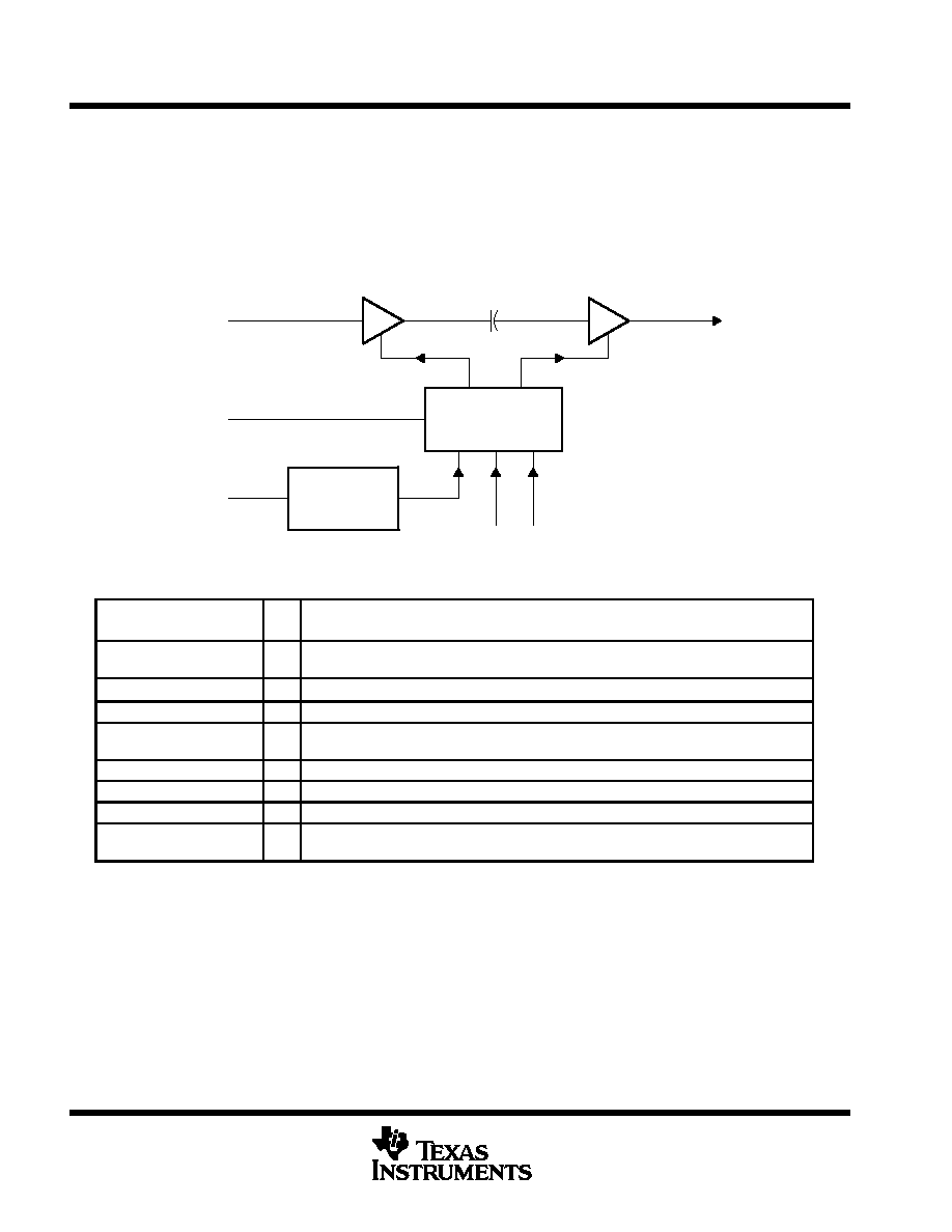
functional block diagram
Bias/Band Gap
Reference
Linear Ramp
Control
VCC VBB
RFIN
TXEN
VPC
3
15
6
RFOUT
18
12, 13
9
Terminal Functions
TERMINAL
I/O
DESCRIPTION
NAME
NO.
I/O
DESCRIPTION
GND
1, 2, 4, 7, 10, 11,
14, 16, 17, 19, 20
Analog ground for all internal analog circuits. All signals are referenced to the ground terminals.
NC
5, 8
No connection. It is recommended that all NC terminals be connected to ground.
RFIN
3
I
RF input. RFIN accepts signals between 800 MHz and 1000 MHz.
RFOUT
18
O
RF output. RFOUT is an open-collector output and requires a decoupled connection to VCC
for operation.
TXEN
15
I
Transmit enable input (digital). When TXEN is high, the output device is enabled.
VBB
9
Control section supply voltage.
VCC
12, 13
First stage bias.
VPC
6
I
Voltage power control. VPC is a signal between 0 V and 3 V that adjusts the output power from
a typical value of ş54 dBm to the maximum output power appropriate for the application.
PowerPAD is a trademark of Texas Instruments Incorporated.
TRF8010
900-MHz RF TRANSMIT DRIVER
SLWS031B ş JULY 1996ş REVISED MAY 1997
3
POST OFFICE BOX 655303
Ě
DALLAS, TEXAS 75265
absolute maximum ratings over operating free-air temperature range (unless otherwise noted)
Supply voltage range, V
CC
(see Note 1)
ş 0.6 V to 5.6 V
. . . . . . . . . . . . . . . . . . . . . . . . . . . . . . . . . . . . . . . . . . . . . .
Input voltage range at TXEN, VPC
ş 0.6 V to 5.6 V
. . . . . . . . . . . . . . . . . . . . . . . . . . . . . . . . . . . . . . . . . . . . . . . . . .
Input power at RFIN
10 dBm
. . . . . . . . . . . . . . . . . . . . . . . . . . . . . . . . . . . . . . . . . . . . . . . . . . . . . . . . . . . . . . . . . . . . .
Thermal resistance, junction to case, R
JC
(see Note 2)
3.5
░
C/W
. . . . . . . . . . . . . . . . . . . . . . . . . . . . . . . . . . . . . .
Thermal resistance, junction to ambient, R
JA
(see Note 3)
32
░
C/W
. . . . . . . . . . . . . . . . . . . . . . . . . . . . . . . . . . .
Continuous total power dissipation at T
A
= 25
_
C
3.9 W
. . . . . . . . . . . . . . . . . . . . . . . . . . . . . . . . . . . . . . . . . . . . . . .
Operating junction temperature, T
J
110
░
C
. . . . . . . . . . . . . . . . . . . . . . . . . . . . . . . . . . . . . . . . . . . . . . . . . . . . . . . . . .
Junction temperature, T
J
max
150
░
C
. . . . . . . . . . . . . . . . . . . . . . . . . . . . . . . . . . . . . . . . . . . . . . . . . . . . . . . . . . . . . .
Operating free-air temperature range, T
A
ş40
░
C to 85
░
C
. . . . . . . . . . . . . . . . . . . . . . . . . . . . . . . . . . . . . . . . . . . . .
Storage temperature range, T
stg
ş65
░
C to 100
░
C
. . . . . . . . . . . . . . . . . . . . . . . . . . . . . . . . . . . . . . . . . . . . . . . . . . . .
Stresses beyond those listed under "absolute maximum ratings" may cause permanent damage to the device. These are stress ratings only, and
functional operation of the device at these or any other conditions beyond those indicated under "recommended operating conditions" is not
implied. Exposure to absolute-maximum-rated conditions for extended periods may affect device reliability.
NOTES:
1. Voltage values are with respect to GND.
2. No air flow and with infinite heatsink
3. With the thermal pad of the device soldered to a 1-ounce copper (Cu) ground plane on an FR4 board with no air flow
recommended operating conditions
MIN
NOM
MAX
UNIT
Supply voltage, VCC (see Note 1)
3
5
V
High-level input voltage at TXEN, VIH
VCC ş 0.8
V
Low-level input voltage at TXEN, VIL
0.8
V
Operating free-air temperature, TA
ş 40
85
░
C
NOTE 1: Voltage values are with respect to GND.
electrical characteristics over full range of operating conditions
supply current, V
CC
= 3.6 V
PARAMETER
TEST CONDITIONS
MIN
TYP
MAX
UNIT
ICC
Supply current from VCC
Operating at maximum power out
TXEN high, VPC = 3 V
163
mA
ICC
Supply current from VCC
Operating at minimum power out
TXEN high, VPC = 0 V
7
mA
Typical values are at TA = 25
_
C.
supply current, V
CC
= 4.8 V
PARAMETER
TEST CONDITIONS
MIN
TYP
MAX
UNIT
Operating at maximum power out
TXEN high, VPC = 3 V
155
210
mA
ICC
Supply current from VCC
Operating at minimum power out
TXEN high, VPC = 0 V
7
mA
Power down
TXEN low, VPC = 0 V
0.05
mA
Typical values are at TA = 25
_
C.
TRF8010
900-MHz RF TRANSMIT DRIVER
SLWS031B ş JULY 1996ş REVISED MAY 1997
4
POST OFFICE BOX 655303
Ě
DALLAS, TEXAS 75265
AMPS/NADC operation, V
CC
= 3.6 V, TXEN high, VPC = 3 V, T
A
= 25
░
C (unless otherwise noted)
PARAMETER
TEST CONDITIONS
MIN
TYP
MAX
UNIT
Operating frequency range
824
849
MHz
PO
Output power
PI = 0 dBm
21
dBm
PO
Output power
PI = 0 dBm
VPC = 0 V
ş58
dBm
Gain (small signal)
PI = ş 20 dBm
27
dB
Power added efficiency (PAE)
PI = 0 dBm
28%
Input return loss (internally matched)
PI = ş 20 dBm
11
dB
Output return loss (externally matched, small signal)
PI = ş 20 dBm
11
dB
Noise power in 30 kHz bandwidth
45 MHz offset at PI = 0 dBm
ş 97
dBm
Harmonics
2f0
PI = 0 dBm
ş 20
dBc
Harmonics
3f0
PI = 0 dBm
ş 50
dBc
G S M o p e r a t i o n , V
CC
= 4.8 V, TXEN high, VPC = 3 V, T
A
= 25
░
C (unless otherwise noted)
PARAMETER
TEST CONDITIONS
MIN
TYP
MAX
UNIT
Extended GSM operating frequency range
870
925
MHz
PO
Output power
PI = 0 dBm
21.5
23
24.5
dBm
PO
Output power
PI = 0 dBm
VPC = 0 V
ş 54
dBm
G a i n ( s m a l l s i g n a l )
PI = ş 20 dBm
28
dB
Power added efficiency (PAE)
PI = 0 dBm
29%
Input return loss (internally matched)
PI = ş 20 dBm
11
dB
Output return loss (externally matched, small signal)
PI = ş20 dBm
11
dB
Harmonics
2f0
PI = 0 dBm
ş 28
ş 22
dBc
Harmonics
3f0
PI = 0 dBm
ş 40
ş 35
dBc
Noise power in 30 kHz bandwidth
20 MHz above f0
PI = 0 dBm
ş 95
dBm
Noise power in 30 kHz bandwidth
10 MHz above f0
PI = 0 dBm
ş 96
dBm
s t a b i l i t y, A M P S / N A D C a n d G S M o p e r a t i o n
PA R A M E T E R
T E S T C O N D I T I O N S
M I N
T Y P
M A X
U N I T
S t a b i l i t y
O u t p u t V S W R
< 6 : 1 a l l p h a s e s ,
VCC < 5.6 V,
PI = 0 dBm,
PO
22 dBm,
Output frequency band: 200 MHz ş 1200 MHz
VSWR = voltage standing wave ratio
No parasitic oscillations (all spurious < ş70 dBc)
switching characteristics
AMPS/NADC and GSM operation, V
CC
= 3.6 V or 4.8 V, T
A
= 25
░
C
PARAMETER
TEST CONDITIONS
MIN
TYP
MAX
UNIT
ton
Switching time, RF output OFF to ON
TXEN = high, VPC stepped from 0 V to 3 V
1
Á
s
toff
Switching time, RF output ON to OFF
TXEN = high, VPC stepped from 3 V to 0 V
1
Á
s

TRF8010
900-MHz RF TRANSMIT DRIVER
SLWS031B ş JULY 1996ş REVISED MAY 1997
5
POST OFFICE BOX 655303
Ě
DALLAS, TEXAS 75265
TYPICAL CHARACTERISTICS
Figure 1
25
PI ş Input Power ş dBm
ş20
ş15
ş10
ş5
0
5
20
15
10
5
P
O
ş Output power ş dBm
VCC = 4.8 V
VPC = 3 V
Freq = 900 MHz
OUTPUT POWER
vs
INPUT POWER
25
░
C
85
░
C
ş40
░
C/25
░
C
Figure 2
25
PI ş Input Power ş dBm
ş20
ş15
ş10
ş5
0
5
20
15
10
5
0
P
AE
ş
Power
Added Efficiency ş %
35
30
25
░
C
ş40
░
C
VCC = 4.8 V
VPC = 3 V
Freq = 900 MHz
POWER ADDED EFFICIENCY
vs
INPUT POWER
85
░
C
Figure 3
22
f ş Frequency ş MHz
860
870
880
890
900
940
21.5
21
20.5
20
P
AE
ş
Power
Added Efficiency ş %
23
22.5
VCC = 4.8 V
VPC = 3 V
PI = 0 dBm
OUTPUT POWER AND POWER
ADDED EFFICIENCY
vs
FREQUENCY
P
O
ş Output Power ş dBm
30
28
26
24
22
34
32
25
░
C
ş40
░
C
85
░
C
ş40
░
C
25
░
C
85
░
C
PAE
PO
910
920
930