Äîêóìåíòàöèÿ è îïèñàíèÿ www.docs.chipfind.ru
TRF7610
SILICON MOSFET POWER AMPLIFIER IC FOR GSM
SLWS059B MAY 1997 REVISED AUGUST 1998
1
POST OFFICE BOX 655303
·
DALLAS, TEXAS 75265
D
Single Positive Power Supply (No Negative
Voltage Required)
D
Advanced Silicon RFMOS
TM
Technology
D
4.8-V Operation for GSM Applications
D
35-dBm Typical Output Power
D
30-dB Typical Power Gain
D
40% Typical PAE with 5-dBm Input Power
D
45% Typical PAE with 8-dBm Input Power
D
Output Power Control
D
Few External Components Required for
Operation
D
Thermally Enhanced Surface-Mount
Package for Small Circuit Footprint
D
Rugged, Sustains 20:1 Load Mismatch
D
800-MHz to 1000-MHz Wide Operational
Frequency Range
D
Low Standby Current (< 10
µ
A)
description
The TRF7610 is a silicon MOSFET power amplifier IC for 900-MHz applications, tailored specifically for global
systems for mobile communications (GSM). It uses Texas Instruments RFMOS
TM
process and consists of a
three-stage amplifier with output power control. Few external components are required for operation.
The TRF7610 amplifies the RF signal from a preceding modulator and the upconverter stages in an RF section
of a transmitter to a level that is sufficient for connection to the antenna. The RF input port, RFIN, and the RF
output port, RFOUT, require simple external matching networks.
A control signal applied to the VPC input can ramp the RF output power up or down to meet ramp and spurious
emission specifications for time-division multiple-access (TDMA) systems. The power control signal causes a
change in output power as the voltage applied to VPC varies between 0 V and 3 V. With the RF input power
applied to RFIN at 5 dBm, adjusting VPC from 0 V to 3 V increases the output power from a typical value of
43 dBm at VPC = 0 V to a typical value of 35 dBm at VPC = 3 V. Forward isolation with the RF input power
applied to RFIN at 5 dBm, VPC = 0 V, is typically 48 dB.
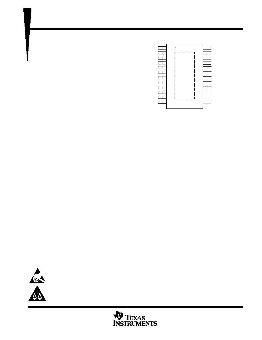
The TRF7610 is available in a thermally enhanced, surface-mount, 24-pin PowerPAD
TM
(PWP) thin-shrink
small-outline package (TSSOP). It is characterized for operation from 40
°
C to 85
°
C operating free-air
temperature. In order to maintain acceptable thermal operating conditions, the device should be operated in
pulse applications such as the GSM standard 1/8 duty cycle. The package has a solderable pad that improves
the package thermal performance by bonding the pad to an external thermal plane. The pad also acts as a
low-inductance electrical path to ground and must be electrically connected to the printed circuit-board (PCB)
ground plane as a continuation of the regular package terminals that are designated GND.
PRODUCTION DATA information is current as of publication date.
Products conform to specifications per the terms of Texas Instruments
standard warranty. Production processing does not necessarily include
testing of all parameters.
Copyright
©
1998, Texas Instruments Incorporated
These devices have limited built-in ESD protection. The leads should be shorted together or the device placed in conductive foam
during storage or handling to prevent electrostatic damage to the MOS gates.
Please be aware that an important notice concerning availability, standard warranty, and use in critical applications of
Texas Instruments semiconductor products and disclaimers thereto appears at the end of this data sheet.
1
2
3
4
5
6
7
8
9
10
11
12
24
23
22
21
20
19
18
17
16
15
14
13
VG2
VG3
VPC
VG1
NC
RFIN
RFIN
NC
VG1
VPC
VG3
VG2
VD1/VD2
GND
RFOUT/VD3
RFOUT/VD3
RFOUT/VD3
RFOUT/VD3
RFOUT/VD3
RFOUT/VD3
RFOUT/VD3
RFOUT/VD3
GND
VD1/VD2
PWP PACKAGE
(TOP VIEW)
NC No internal connection
RFMOS and PowerPAD are trademarks of Texas Instruments Incorporated.
TRF7610
SILICON MOSFET POWER AMPLIFIER IC FOR GSM
SLWS059B MAY 1997 REVISED AUGUST 1998
2
POST OFFICE BOX 655303
·
DALLAS, TEXAS 75265
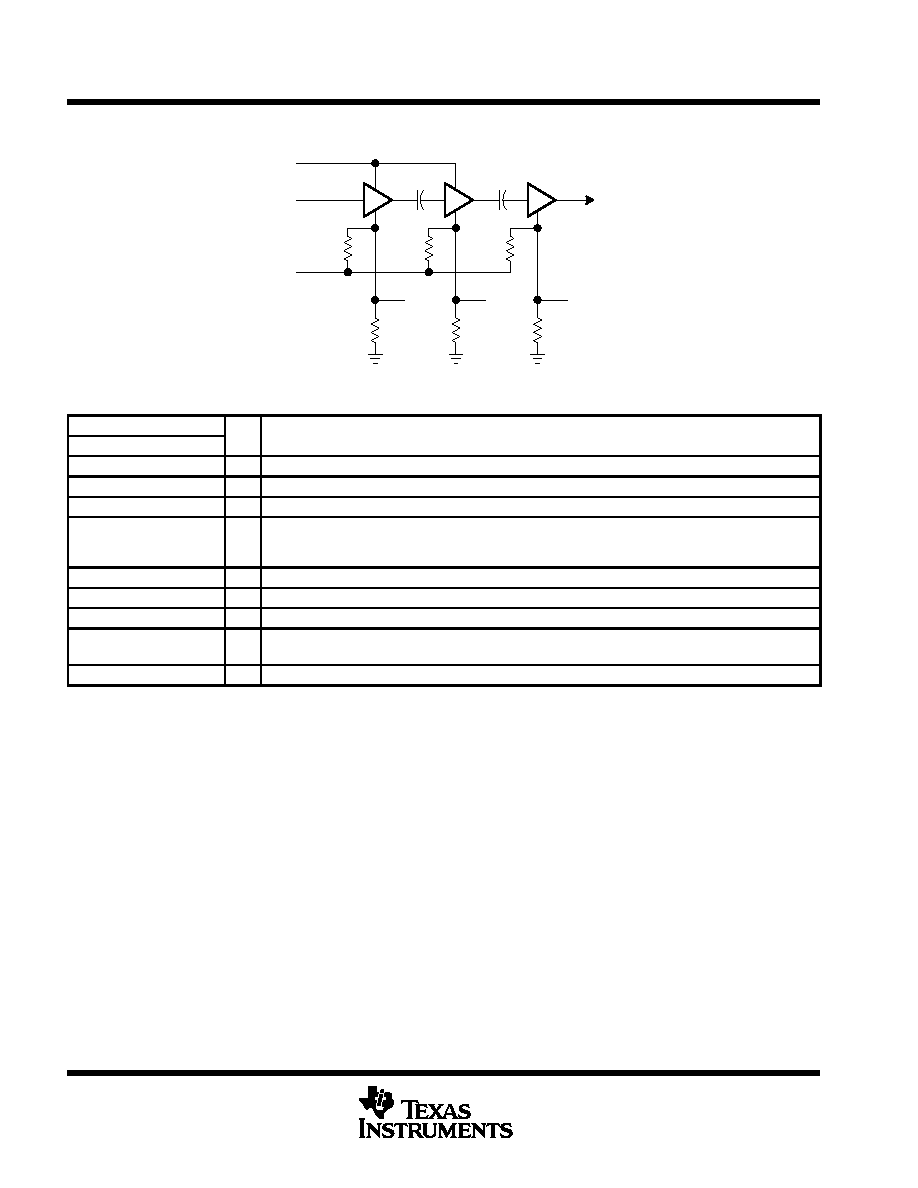
schematic
VD1/VD2
13, 24
RFIN
15 22
RFOUT/VD3
4 or 9
VG1
1, 12
VG2
2 or 11
VG3
3 or 10
VPC
6, 7
Terminal Functions
TERMINAL
I/O
DESCRIPTION
NAME
NO.
I/O
DESCRIPTION
GND
14, 23
Analog ground for all internal circuits. All signals are referenced to the ground terminals.
NC
5, 8
No internal connection. It is recommended that all NC terminals be connected to ground.
RFIN
6, 7
I
RF input. RFIN accepts signals between 800 MHz and 1000 MHz.
RFOUT/ VD3
15, 16, 17,
18, 19, 20,
21, 22
I/O
RF output and third
-
stage drain bias. RFOUT requires an external matching network.
VG1
4, 9
I
First
-
stage gate bias set by resistor. Either terminal may be used or both may be connected externally.
VG2
1, 12
I
Second
-
stage gate bias set by resistor. These terminals must be connected externally.
VG3
2, 11
I
Third
-
stage gate bias set by resistor. Either terminal may be used or both may be connected externally.
VPC
3, 10
I
Voltage power control. VPC is a signal between 0 V and 3 V that adjusts the output power from a typical
value of 43 dBm to 35 dBm. Either terminal may be used, or both may be connected externally.
VD1/ VD2
13, 24
I
First
-
and second
-
stage drain bias. These terminals must be connected externally.
absolute maximum ratings over operating free-air temperature range (unless otherwise noted)
Supply voltage range, V
DD
(see Note 1)
0.6 V to 8 V
. . . . . . . . . . . . . . . . . . . . . . . . . . . . . . . . . . . . . . . . . . . . . . .
Input voltage range, VPC
0.6 V to 4 V
. . . . . . . . . . . . . . . . . . . . . . . . . . . . . . . . . . . . . . . . . . . . . . . . . . . . . . . . . . . .
Input power at RFIN
13 dBm
. . . . . . . . . . . . . . . . . . . . . . . . . . . . . . . . . . . . . . . . . . . . . . . . . . . . . . . . . . . . . . . . . . . . .
Thermal resistance, junction to case, R
JC
(see Note 2)
3.5
°
C/W
. . . . . . . . . . . . . . . . . . . . . . . . . . . . . . . . . . . . . .
Junction temperature, T
J
max
150
°
C
. . . . . . . . . . . . . . . . . . . . . . . . . . . . . . . . . . . . . . . . . . . . . . . . . . . . . . . . . . . . . .
Operating free-air temperature range, T
A
40
°
C to 85
°
C
. . . . . . . . . . . . . . . . . . . . . . . . . . . . . . . . . . . . . . . . . . . . . . . . . .
Storage temperature range, T
stg
65
°
C to 150
°
C
. . . . . . . . . . . . . . . . . . . . . . . . . . . . . . . . . . . . . . . . . . . . . . . . . . . .
Stresses beyond those listed under "absolute maximum ratings" may cause permanent damage to the device. These are stress ratings only, and
functional operation of the device at these or any other conditions beyond those indicated under "recommended operating conditions" is not
implied. Exposure to absolute-maximum-rated conditions for extended periods may affect device reliability.
NOTES:
1. Voltage values are with respect to GND.
2. No air flow and with infinite heatsink
TRF7610
SILICON MOSFET POWER AMPLIFIER IC FOR GSM
SLWS059B MAY 1997 REVISED AUGUST 1998
3
POST OFFICE BOX 655303
·
DALLAS, TEXAS 75265
recommended operating conditions
PARAMETER
MIN
NOM
MAX
UNIT
Supply voltage VDD (see Note 1 and Note 3)
3.5
4.8
6
V
Operating free-air temperature, TA
40
85
°
C
Operating frequency range (see Note 4)
800
1000
MHz
NOTES:
1. Voltage values are with respect to GND.
3 .Performance varies with drain voltage, see Figure 8.
4. External matching network dependent.
electrical characteristics over full range of recommended operating conditions
supply current, V
DD
= 4.8 V
PARAMETER
TEST CONDITIONS
MIN
TYP
MAX
UNIT
IDD Supply current
Operating at maximum output power
VPC = 3 V
2
A
IDD Supply current
Operating with no RF input power
VPC = 0 V
< 10
µ
A
Typical values are at TA = 25
°
C
GSM operation, V
DD
= 4.8 V, VPC = 3 V, P
I
= 5 dBm, T
A
= 25
°
C (unless otherwise noted)
PARAMETER
TEST CONDITIONS
MIN
TYP
MAX
UNIT
Operating frequency range
870
925
MHz
Output power
VPC = 3 V
34
35
36
dBm
Output power
VPC = 0 V
43
dBm
Power added efficiency (PAE)
40%
Power added efficiency (PAE)
PI = 8 dBm
45%
Input return loss (externally matched, small signal)
PI = 20 dBm
10
dB
Harmonics
2f0
With external matching
28
dBc
Harmonics
3f0
With external matching
40
dBc
Noise power in 30
-
kHz bandwidth
20 MHz above f0
88
dBm
Noise power in 30
-
kHz bandwidth
10 MHz above f0
88
dBm
Ruggedness test
Frequency = 900 MHz,
Load VSWR = 20:1,
All phase angles
§
Specific applications circuit
§ No degradation in output power after test.
stability, GSM operation
PARAMETER
TEST CONDITIONS
MIN
TYP
MAX
UNIT
Stability
Output VSWR¶ < 6:1 all phases, VDD < 6 V, P
I
= 5 dBm,
PO
35 dBm, Output frequency band: 200 MHz 1200 MHz
No parasitic
oscillations (all
spurious < 70 dBc)
¶ VSWR = voltage standing wave ratio
switching characteristics
GSM operation
PARAMETER
TEST CONDITIONS
MIN
TYP
MAX
UNIT
ton
Switching time, RF output OFF to ON
VPC stepped from 0 V to 3 V
2
µ
s
toff
Switching time, RF output ON to OFF
VPC stepped from 3 V to 0 V
2
µ
s
TRF7610
SILICON MOSFET POWER AMPLIFIER IC FOR GSM
SLWS059B MAY 1997 REVISED AUGUST 1998
4
POST OFFICE BOX 655303
·
DALLAS, TEXAS 75265
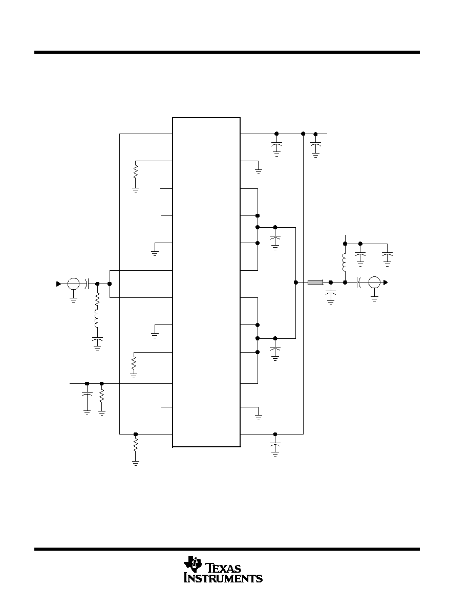
APPLICATION INFORMATION
In all cases, a capacitor must be connected from the positive power supply to ground as close to the terminals as
possible for power-supply bypassing. The dc-blocking capacitors are required on the RF input and RF output. A list
of components and their functions is shown in Table 1.
VG2
VG3
VPC
VG1
NC
RFIN
RFIN
NC
VG1
VPC
VG3
VG2
VD1/VD2
GND
RFOUT/VD3
RFOUT/VD3
RFOUT/VD3
RFOUT/VD3
RFOUT/VD3
RFOUT/VD3
RFOUT/VD3
RFOUT/VD3
GND
VD1/VD2
24
23
22
21
20
19
18
17
16
15
14
13
1
2
3
4
5
6
7
8
9
10
11
12
C5
C6
VD1/VD2
C4
C7
C8
C10
VD3
C9
RFOUT
R1
R3
R2
C2
C1
RFIN
C12
VPC
TRF7610
R4
L1
R5
C11
C3
245 mil
50
L2
+
+
Figure 1. Typical GSM Cellular Telephone Application
TRF7610
SILICON MOSFET POWER AMPLIFIER IC FOR GSM
SLWS059B MAY 1997 REVISED AUGUST 1998
5
POST OFFICE BOX 655303
·
DALLAS, TEXAS 75265
Table 1. External Component Selection
COMPONENT
DESIGNATION
TYPICAL VALUE
FUNCTION
C1
100 pF
DC blocking capacitor
C2
100 pF
Matching capacitor
C3
330
µ
F
Drain-bias decoupling capacitor
C4
0.033
µ
F
Drain-bias decoupling capacitor
C5, C6
22 pF
High-Q matching capacitor
C7
0.033
µ
F
Drain-bias decoupling capacitor
C8
11 pF
High-Q matching capacitor
C9
100 pF
DC blocking capacitor
C10
100 pF
Drain-bias decoupling capacitor
C11
100
µ
F
Drain-bias decoupling capacitor
C12
100 pF
Decoupling capacitor
R1
2200
Gate-bias setting resistor
R2, R3
5100
Gate-bias setting resistor
R4
3.9
Matching resistor
R5
51
Vpc termination resistor
L1
2.7 nH
Matching inductor
L 2
18.5 nH high-current inductor
or
/4 microstrip line
Drain bias inductor
On a FR4 substrate with
r of 4.3, a
/4 50
line is 40 mm.
design philosophy
The TRF7610 is a three-stage integrated power amplifier for use in cellular phone handsets. The device and
applications board are optimized to operate under 900-MHz, 4.8-V GSM conditions. External matching
networks provide design flexibility in centering the frequency response from 800 to 1000 MHz. Typical
performance at 900 MHz, driven by a 5-dBm GSM signal, is 30 dB of power gain, 35 dBm output power, and
40 percent PAE.
Discrete component selection was made to optimize output power, gain, pulse flatness in the GSM pulse
window, and PAE. Where possible, size and cost goals were considered: the smallest, least expensive
components available were included in the applications board design. Some of the components, however, were
chosen for their ability to increase performance. The following sections explain the design options and
compromises to consider when substituting parts of differents types and values.
output matching network
The output matching network provides the majority of the design flexibility. First, the shunt capacitors, C5, C6,
and C8 are American Technical Ceramics high-Q capacitors, which increase performance. The ATC capacitors
achieve a 0.4-dB increase in output power and a 3-percent increase in PAE compared to the performance
achieved using 0402-sized capacitors. However, if size and cost are more important, 0402-sized capacitors can
be used, while sacrificing the performance gains achieved using the high-Q capacitors.
Second, the dc bias network on the amplifier output stage, designed using a Coilcraft 18.5 nH high-current
inductor (L 2), minimizes the board layout area. An alternative to this high-current inductor is a quarter-wave stub
with a bias decoupling capacitor to ground (C10, C3). On the FR4 board with
r
= 4.3, a quarter-wave stub at
900 MHz is 40 mm in length. One advantage that the quarter-wave stub offers over the inductor is improved
second harmonic suppression. The inductor offers a much smaller footprint; however, it does sacrifice 10 dB
TRF7610
SILICON MOSFET POWER AMPLIFIER IC FOR GSM
SLWS059B MAY 1997 REVISED AUGUST 1998
6
POST OFFICE BOX 655303
·
DALLAS, TEXAS 75265
of second harmonic suppression. The PAE is only slightly affected: it is reduced by approximately 1 percent
compared to the quarter-wave stub. The system designer must decide if size or performance is of greatest
concern.
The 330
µ
F bias decoupling capacitors, C3 and C11, provide pulse flatness in the GSM application. These
surface mount capacitors provide a gain slope of 0.4 dB over the duration of the GSM duty cycle. If that is not
acceptable, the performance can be improved by adding a larger value capacitor in parallel with the two existing
capacitors. Measured results, using a standard 4700
µ
F electrolytic taken from a cellular phone, is 0.1 dB of
gain slope for the duration of the GSM duty cycle. Capacitor size considerations must be decided by the system
designer.
dc bias network
The dc bias network consists of resistors R1, R2, R3, and R5, which set the gate bias voltage of the device. R1,
R2, and R3 are used as voltage divider resistors which set the gate voltages at approximately 1.7 V. Resistor
R5 is a 51
termination resistor that is needed only for a 50
pulse generator. When a high-impedance pulse
generator is used, the 51
resistor can be omitted as it is not necessary for device function.
TRF7610
SILICON MOSFET POWER AMPLIFIER IC FOR GSM
SLWS059B MAY 1997 REVISED AUGUST 1998
7
POST OFFICE BOX 655303
·
DALLAS, TEXAS 75265
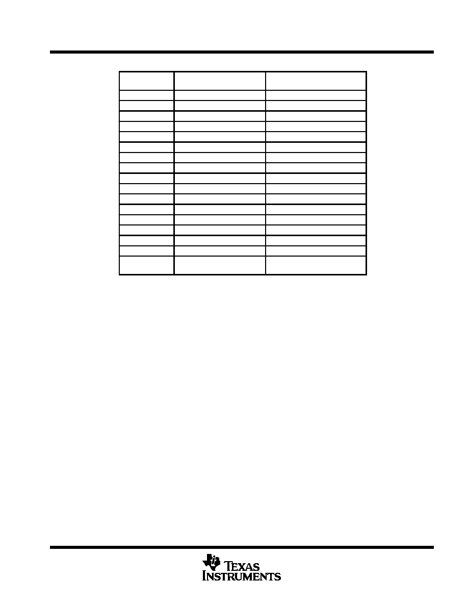
TYPICAL CHARACTERISTICS
Figure 2
25
15
10
0
20
15
10
5
P
AE
Power
Added Efficiency %
35
45
PI Input Power dBm
POWER ADDED EFFICIENCY
vs
INPUT POWER
50
0
5
10
40
30
20
5
Frequency = 900 MHz
VDD = 4.8 V
VPC = 3 V Pulsed
TA = 40
°
C
TA = 85
°
C
TA = 25
°
C
Figure 3
PI = 5 dBm
VDD = 4.8 V
VPC = 3 V Pulsed
TA = 40
°
C
TA = 85
°
C
TA = 25
°
C
30
25
15
5
850 860 870 880 890 900 910
P
AE
Power
Added Efficiency %
40
50
f Frequency MHz
55
920 930 940 950
45
35
20
10
POWER ADDED EFFICIENCY
vs
FREQUENCY
Figure 4
30
20
10
5
2.5
3
3.5
4
4.5
40
50
60
5
5.5
6
TA = 40
°
C
TA = 85
°
C
TA = 25
°
C
POWER ADDED EFFICIENCY
vs
DRAIN VOLTAGE
Frequency = 900 MHz
PI = 5 dBm
VPC = 3 V Pulsed
VDD Drain Voltage V
P
AE
Power
Added Efficiency %
Figure 5
TA = 85
°
C
TA = 25
°
C
POWER ADDED EFFICIENCY
vs
POWER CONTROL VOLTAGE
Frequency = 900 MHz
VDD = 4.8 V
PI = 5 dBm
TA = 40
°
C
25
15
5
5
0
0.5
1
1.5
2
30
45
VPC Power Control Voltage V
50
2.5
3
40
35
20
10
0
P
AE
Power
Added Efficiency %
TRF7610
SILICON MOSFET POWER AMPLIFIER IC FOR GSM
SLWS059B MAY 1997 REVISED AUGUST 1998
8
POST OFFICE BOX 655303
·
DALLAS, TEXAS 75265
TYPICAL CHARACTERISTICS
Figure 6
TA = 85
°
C
TA = 25
°
C
OUTPUT POWER
vs
INPUT POWER
Frequency = 900 MHz
VDD = 4.8 V
VPC = 3 V Pulsed
20
15
5
0
20
15
10
5
PO Output Power dBm
25
35
PI Input Power dBm
40
0
5
10
30
10
TA = 40
°
C
Figure 7
TA = 40
°
C
TA = 85
°
C
TA = 25
°
C
OUTPUT POWER
vs
FREQUENCY
PI = 5 dBm
VDD = 4.8 V
VPC = 3 V Pulsed
34
33
31
30
850 860 870 880 890 900 910
PO Output Power dBm
35
37
f Frequency MHz
38
920 930
940 950
36
32
Figure 8
20
15
10
0
2.5
3
3.5
4
4.5
PO Output Power dBm
25
35
40
5
5.5
6
TA = 40
°
C
TA = 85
°
C
TA = 25
°
C
OUTPUT POWER
vs
DRAIN VOLTAGE
Frequency = 900 MHz
PI = 5 dBm
VPC = 3 V Pulsed
30
5
VDD Drain Voltage V
Figure 9
10
10
20
30
0
0.5
1
1.5
2
20
30
VPC Power Control Voltage V
40
2.5
3
TA = 40
°
C
TA = 85
°
C
TA = 25
°
C
OUTPUT POWER
vs
POWER CONTROL VOLTAGE
Frequency = 900 MHz
VDD = 4.8 V
VPC = 3 V Pulsed
PO Output Power dBm
0
TRF7610
SILICON MOSFET POWER AMPLIFIER IC FOR GSM
SLWS059B MAY 1997 REVISED AUGUST 1998
9
POST OFFICE BOX 655303
·
DALLAS, TEXAS 75265
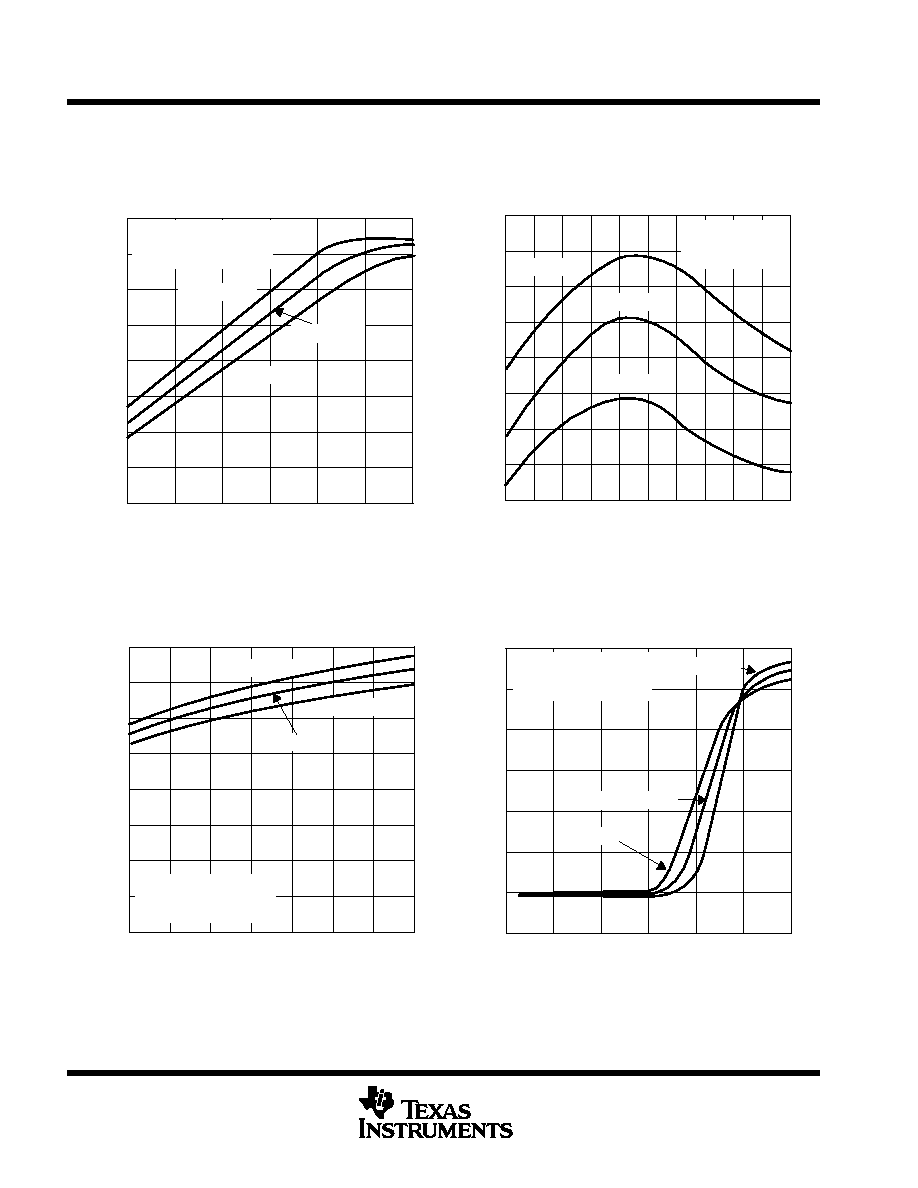
TYPICAL CHARACTERISTICS
Figure 10
6
8
10
12
700
800
900
S1
1 Input Return Loss dB
4
2
f Frequency MHz
INPUT RETURN LOSS
vs
FREQUENCY
0
1000
1100
VDD = 4.8 V
VPC = 3 V
PI = 5 dBm
TA = 25
°
C
Matched Application Board
Figure 11
25
15
10
0
850 860 870 880 890 900 910
30
45
f Frequency MHz
SMALL SIGNAL GAIN
vs
FREQUENCY
50
920 930 940 950
40
35
20
5
TA = 40
°
C
TA = 85
°
C
TA = 25
°
C
S21 Small Signal Gain dB
VDD = 4.8 V
VPC = 3 V
Matched Application Board
TRF7610
SILICON MOSFET POWER AMPLIFIER IC FOR GSM
SLWS059B MAY 1997 REVISED AUGUST 1998
10
POST OFFICE BOX 655303
·
DALLAS, TEXAS 75265
MECHANICAL DATA
PWP (R-PDSO-G**)
PowerPAD
TM
PLASTIC SMALL-OUTLINE PACKAGE
0,25
0,50
0,75
0,15 NOM
Gage Plane
4073225/E 03/97
6,60
6,20
0,30
0,19
11
4,30
4,50
10
20
A
1
1,20 MAX
Seating Plane
0
°
8
°
Thermal Pad (3,18
2,41 NOM)
(see Note C)
0,10
0,65
M
0,10
28
9,80
24
7,90
9,60
7,70
16
5,10
14
5,10
4,90
4,90
DIM
A MAX
A MIN
PINS **
6,40
6,60
20
0,15
0,05
NOTES: A. All linear dimensions are in millimeters.
B. This drawing is subject to change without notice.
C. The package thermal performance may be enhanced by bonding the thermal pad to an external thermal plane. This solderable pad
is electrically and thermally connected to the backside of the die.

IMPORTANT NOTICE
Texas Instruments and its subsidiaries (TI) reserve the right to make changes to their products or to discontinue
any product or service without notice, and advise customers to obtain the latest version of relevant information
to verify, before placing orders, that information being relied on is current and complete. All products are sold
subject to the terms and conditions of sale supplied at the time of order acknowledgement, including those
pertaining to warranty, patent infringement, and limitation of liability.
TI warrants performance of its semiconductor products to the specifications applicable at the time of sale in
accordance with TI's standard warranty. Testing and other quality control techniques are utilized to the extent
TI deems necessary to support this warranty. Specific testing of all parameters of each device is not necessarily
performed, except those mandated by government requirements.
CERTAIN APPLICATIONS USING SEMICONDUCTOR PRODUCTS MAY INVOLVE POTENTIAL RISKS OF
DEATH, PERSONAL INJURY, OR SEVERE PROPERTY OR ENVIRONMENTAL DAMAGE ("CRITICAL
APPLICATIONS"). TI SEMICONDUCTOR PRODUCTS ARE NOT DESIGNED, AUTHORIZED, OR
WARRANTED TO BE SUITABLE FOR USE IN LIFE-SUPPORT DEVICES OR SYSTEMS OR OTHER
CRITICAL APPLICATIONS. INCLUSION OF TI PRODUCTS IN SUCH APPLICATIONS IS UNDERSTOOD TO
BE FULLY AT THE CUSTOMER'S RISK.
In order to minimize risks associated with the customer's applications, adequate design and operating
safeguards must be provided by the customer to minimize inherent or procedural hazards.
TI assumes no liability for applications assistance or customer product design. TI does not warrant or represent
that any license, either express or implied, is granted under any patent right, copyright, mask work right, or other
intellectual property right of TI covering or relating to any combination, machine, or process in which such
semiconductor products or services might be or are used. TI's publication of information regarding any third
party's products or services does not constitute TI's approval, warranty or endorsement thereof.
Copyright
©
1998, Texas Instruments Incorporated