TRF3040
MODULATOR/SYNTHESIZER
SLWS057 AUGUST 1999
1
POST OFFICE BOX 655303
·
DALLAS, TEXAS 75265
D
2-GHz Main Synthesizer, Which
Incorporates a Dual-Mode 32/33 and 64/65
Prescaler for Fractional-N Operation
D
200-MHz Auxiliary Synthesizer, Which
Incorporates an 8/9 Prescaler
D
Separate Supply Terminals for Main and
Auxiliary Charge Pumps
D
Internal Compensation for Fractional Spurs
D
Low Phase Noise
D
Normal and Integral Charge Pump Outputs
D
Fully Programmable Main and Auxiliary
Dividers
D
Serial Data Interface
D
Direct I/Q Modulator
D
Control Logic for Power-Down Modes
D
Single-Sideband Suppressed Carrier
(SSBSC) Converter to Generate TX Carrier
D
200-MHz TXIF Synthesizer and Oscillator
D
Variable Gain Amplifier (VGA) With 50 dB of
Dynamic Range
D
900-MHz Power Amplifier (PA) Driver With
9 dBm Typical Output Power
D
Reference and Clock Buffers
D
158 mA Typical Total Operating Current at
3.75 V Supply
D
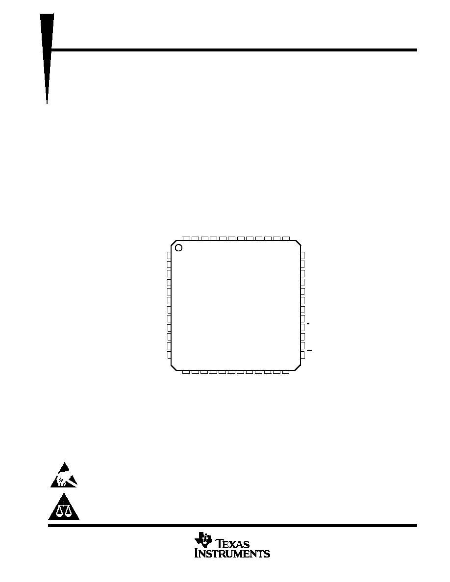
48-Pin Quad Flatpack (LQFP)
14 15
XTAL
TXEN
DATA
CLOCK
LOCK
STROBE
V
SSA
V
DD
I
I
Q
Q
36
35
34
33
32
31
30
29
28
27
26
25
16
1
2
3
4
5
6
7
8
9
10
11
12
PHP
V
DDA
RXLO+
RXLO
V
SSA
V
CCP
TXLO+
TXLO
V
SSP
PHSOUT
IPEAK
TANK+
17 18 19 20
PHA
RCLK
MCLK
47 46 45 44 43
48
42
PHI
RF
RN
V
GND
40 39 38
41
21 22 23 24
37
13
INA
RA
T
ANK
V
DDA
DUAL
TX+
DUAL
TX
V
DDA
V
DDA
V
DDA
XT
AL+
PT PACKAGE
(TOP VIEW)
SS
V
SSA
V
SSA
V
SSA
V
SSA
V
SSA
V
SSA
These devices have limited built-in ESD protection. The leads should be shorted together or the device placed in conductive foam
during storage or handling to prevent electrostatic damage to the MOS gates.
Please be aware that an important notice concerning availability, standard warranty, and use in critical applications of
Texas Instruments semiconductor products and disclaimers thereto appears at the end of this data sheet.
PRODUCTION DATA information is current as of publication date.
Products conform to specifications per the terms of Texas Instruments
standard warranty. Production processing does not necessarily include
testing of all parameters.
Copyright
©
1999, Texas Instruments Incorporated
TRF3040
MODULATOR/SYNTHESIZER
SLWS057 AUGUST 1999
2
POST OFFICE BOX 655303
·
DALLAS, TEXAS 75265
description
The TRF3040 is an integrated transmit modulator/synthesizer circuit suitable for 900-MHz analog and digital
cellular telephones. It consists of a transmit intermediate frequency (TXIF) synthesizer and oscillator, a
single-sideband suppressed carrier (SSBSC) converter, a direct conversion I/Q modulator, a variable gain
amplifier (VGA) with a power amplifier (PA) driver, a main channel fractional-N synthesizer, an auxiliary
channel synthesizer, a crystal oscillator reference buffer, and clock buffers in a small surface-mount
package. Very few external components are required.
The TXIF synthesizer produces the offset signal, TXIF, needed to translate the external local oscillator
(TXLO) signal to the correct transmission frequency. The TXIF_VCO (voltage controlled oscillator) can
operate from 90 MHz to 200 MHz, depending on the component values chosen for the external tank circuit.
The TXLO signal may be differential or single-ended input.
The direct conversion I/Q modulator places the modulation signal (
/4-DQPSK, FM) directly on top of the
transmit carrier frequency.
The VGA has an output range of 41 dBm to 9 dBm into a 200-
differential load. The balanced output signal
simplifies the board layout making it easier to meet isolation requirements.

TRF3040
MODULATOR/SYNTHESIZER
SLWS057 AUGUST 1999
3
POST OFFICE BOX 655303
·
DALLAS, TEXAS 75265
functional block diagram
TXIF_
VCO
N
(N = 6, 7, 8, 9)
TXIF
TXIF_LD
+ 90
+ 90
+
+
+ 90
Control Logic
Main
Prescaler
÷
32/33
Main Phase
Detector
Reference
Divider
Auxiliary
Phase Detector
Auxiliary
Divider
Lock
Detect
TXLO +
DUALTX+
I
TXEN
DATA
CLOCK
STROBE
PHP
PHI
LOCK
PHA
+
RXLO
MCLK
RCLK
INA
TXIF_LD
DUALTX
TANK+
TANK
PHSOUT
+
+
12
13
IPEAK
10
11
3
4
38
39
37
43
26
8
7
25
20
22
28
27
35
34
33
31
1
48
32
41
36
INR
Q
Q
XTAL
XTAL
XTAL
OSC
I
+
RCLK Buffer
Main Divider
Main
Prescaler
÷
8/9
Auxiliary Synthesizer
Input Buffer
Reference
Divider Buffer
MCLK Buffer
RXLO Buffer
TXIF
Phase
Detector
and
Charge
Pump
TXIF_VCO
Buffer
TXIF_Buffer
TXLO
BPF
DUALTX
VGA
I/Q Modulator
Transmit Intermediate
Frequency Synthesizer
SSBSC Converter and TXIF Buffer
TXLO_Buffer
TXRF
PA Driver

TRF3040
MODULATOR/SYNTHESIZER
SLWS057 AUGUST 1999
4
POST OFFICE BOX 655303
·
DALLAS, TEXAS 75265
Terminal Functions
TERMINAL
I/O
DESCRIPTION
NAME
NO.
I/O
DESCRIPTION
ÁÁÁÁ
ÁÁÁÁ
CLOCK
ÁÁÁ
ÁÁÁ
33
ÁÁÁ
ÁÁÁ
I
Serial clock input
ÁÁÁÁ
ÁÁÁÁ
DATA
ÁÁÁ
ÁÁÁ
34
ÁÁÁ
ÁÁÁ
I
Serial data input
ÁÁÁÁ
DUALTX +
ÁÁÁ
20
ÁÁÁ
O
Differential RF power amplifier driver
ÁÁÁÁ
ÁÁÁÁ
DUALTX
ÁÁÁ
ÁÁÁ
22
ÁÁÁ
ÁÁÁ
O
Differential RF power amplifier driver
ÁÁÁÁ
ÁÁÁÁ
GND
ÁÁÁ
ÁÁÁ
19
ÁÁÁ
ÁÁÁ
Substrate (GND)
ÁÁÁÁ
ÁÁÁÁ
I
ÁÁÁ
ÁÁÁ
28
ÁÁÁ
ÁÁÁ
I
Baseband inverting in-phase modulation input
ÁÁÁÁ
I
ÁÁÁ
27
ÁÁÁ
I
Baseband noninverting in-phase modulation input
ÁÁÁÁ
ÁÁÁÁ
INA
ÁÁÁ
ÁÁÁ
43
ÁÁÁ
ÁÁÁ
I
Auxiliary synthesizer input
ÁÁÁÁ
ÁÁÁÁ
IPEAK
ÁÁÁ
ÁÁÁ
11
ÁÁÁ
ÁÁÁ
TX offset loop charge pump current setting resistor
ÁÁÁÁ
ÁÁÁÁ
LOCK
ÁÁÁ
ÁÁÁ
32
ÁÁÁ
ÁÁÁ
O
Lock detect output
ÁÁÁÁ
MCLK
ÁÁÁ
38
ÁÁÁ
O
Buffered master clock output
ÁÁÁÁ
ÁÁÁÁ
PHA
ÁÁÁ
ÁÁÁ
41
ÁÁÁ
ÁÁÁ
O
Auxiliary charge pump output
ÁÁÁÁ
ÁÁÁÁ
PHI
ÁÁÁ
ÁÁÁ
48
ÁÁÁ
ÁÁÁ
O
Main charge pump integral output
ÁÁÁÁ
ÁÁÁÁ
PHP
ÁÁÁ
ÁÁÁ
1
ÁÁÁ
ÁÁÁ
O
Main charge pump proportional output
ÁÁÁÁ
ÁÁÁÁ
PHSOUT
ÁÁÁ
ÁÁÁ
10
ÁÁÁ
ÁÁÁ
O
TX offset charge pump output
ÁÁÁÁ
Q
ÁÁÁ
25
ÁÁÁ
I
Baseband inverting quadrature modulation input
ÁÁÁÁ
ÁÁÁÁ
Q
ÁÁÁ
ÁÁÁ
26
ÁÁÁ
ÁÁÁ
I
Baseband noninverting quadrature modulation input
ÁÁÁÁ
ÁÁÁÁ
RA
ÁÁÁ
ÁÁÁ
42
ÁÁÁ
ÁÁÁ
Auxiliary charge pump current setting resistor
ÁÁÁÁ
ÁÁÁÁ
RCLK
ÁÁÁ
ÁÁÁ
39
ÁÁÁ
ÁÁÁ
O
Buffered reference clock output
ÁÁÁÁ
RF
ÁÁÁ
47
Fractional compensation charge pump current setting resistor
ÁÁÁÁ
ÁÁÁÁ
RN
ÁÁÁ
ÁÁÁ
46
Main charge pump current setting resistor
ÁÁÁÁ
ÁÁÁÁ
RXLO +
ÁÁÁ
ÁÁÁ
3
I
Differential main synthesizer positive input
ÁÁÁÁ
ÁÁÁÁ
RXLO
ÁÁÁ
ÁÁÁ
4
I
Differential main synthesizer negative input
ÁÁÁÁ
ÁÁÁÁ
STROBE
31
I
Data strobe input
ÁÁÁÁ
TANK +
12
I
Differential TXIF_VCO tank positive input
ÁÁÁÁ
ÁÁÁÁ
TANK
13
I
Differential TXIF_VCO tank negative input
ÁÁÁÁ
ÁÁÁÁ
TXEN
35
I
Transmit enable
ÁÁÁÁ
ÁÁÁÁ
TXLO +
7
I
Differential transmit LO positive input
ÁÁÁÁ
TXLO
8
I
Differential transmit LO negative input
ÁÁÁÁ
ÁÁÁÁ
VCCP
6
ÁÁÁÁÁÁÁÁÁÁÁÁÁÁÁÁÁÁ
ÁÁÁÁÁÁÁÁÁÁÁÁÁÁÁÁÁÁ
Main charge pump and bandgap supply voltage
VDD
29
Digital supply voltage
2
Main prescaler and bandgap supply voltage
14
TX offset loop supply voltage
VDDA
24
RF modulator supply voltage
40
Oscillator and buffers supply voltage
44
Auxiliary charge pump supply voltage
17, 18
RF modulator ground
5
Main prescaler and bandgap ground
VSSA
15
TX offset loop ground
VSSA
16
TX offset loop and charge pump ground
21, 23
PA driver ground
30
Oscillator, MCLK, and RCLK ground
VSS
45
Digital ground
VSSP
9
Main charge pump ground
XTAL +
37
I
Crystal oscillator base input
XTAL
36
O
Crystal oscillator emitter input
Pins have limited ESD protection
TRF3040
MODULATOR/SYNTHESIZER
SLWS057 AUGUST 1999
5
POST OFFICE BOX 655303
·
DALLAS, TEXAS 75265
absolute maximum ratings over operating free-air temperature range (unless otherwise noted)
Power supply voltage range , V
CCP
, V
DD,
V
DDA
(see Note 1)
0.3 V to 4.5 V
. . . . . . . . . . . . . . . . . . . . . . . . . . .
Voltage applied to any other terminal, V
IN
0.3 V to
V
CC
/V
DD
+ 0.3 V
. . . . . . . . . . . . . . . . . . . . . . . . . . . . . . . . .
Operation junction temperature, T
Jmax
150
°
C
. . . . . . . . . . . . . . . . . . . . . . . . . . . . . . . . . . . . . . . . . . . . . . . . . . . . .
Operating temperature, T
A
40
°
C to 85
°
C
. . . . . . . . . . . . . . . . . . . . . . . . . . . . . . . . . . . . . . . . . . . . . . . . . . . . . . . . .
Storage temperature, T
stg
65
°
C to 150
°
C
. . . . . . . . . . . . . . . . . . . . . . . . . . . . . . . . . . . . . . . . . . . . . . . . . . . . . . . . .
Stresses beyond those listed under "absolute maximum ratings" may cause permanent damage to the device. These are stress ratings only, and
functional operation of the device, at these or any other conditions beyond those indicated under "recommended operating conditions", is not
implied. Exposure to absolute-maximum-rated conditions for extended periods may affect device reliability.
NOTE 1: Voltage values are in respect to VSSA (VSSA = VSSP = VSS = GND)
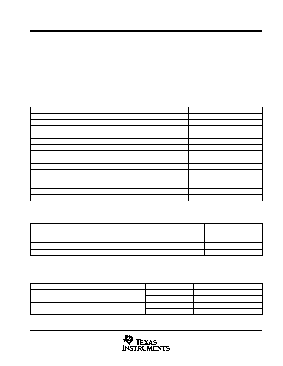
recommended operating conditions
PARAMETER
MIN
NOM
MAX
UNIT
Supply voltage, VCCP, VDD, VDDA
3.6
3.75
3.9
V
High-level input voltage, VIH (CLOCK, DATA, STROBE, TXEN)
0.7
×
VDD
VDD + 0.3
V
Low-level input voltage, VIL (CLOCK, DATA, STROBE, TXEN)
0.3
0.3
×
VDD
V
Main synthesizer input frequency, fIN(RXLO
±
)
2000
MHz
Main synthesizer input power, PIN(RXLO
±
), (AC coupled, 50-
single ended, 100-
differential)
17
dBm
Transmit LO input frequency, fIN(TXLO
±
)
1050
MHz
Transmit LO input power, PIN(TXLO
±
), (AC coupled, 50-
single ended, 100-
differential)
10
dBm
TXIF_VCO tank differential input frequency, fIN(TANK
±
)
200
MHz
Crystal oscillator input frequency, fIN(XTAL+)
25
MHz
Auxiliary synthesizer input frequency, fIN(INA)
200
MHz
Auxiliary synthesizer input voltage, VIN(INA), (AC coupled)
0.2
VPP
In-phase differential input, I/I (quiescent)
VDDA/2
V
Quadraphase differential input, Q/Q (quiescent)
VDDA/2
V
Operating free-air temperature, TA
40
25
85
°
C
dc electrical characteristics V
CCP
= V
DD
= V
DDA
= 3.75 V, T
A
= 25
°
C (unless otherwise noted)
supply current I = I
CCP
+ I
DD
+ I
DDA
PARAMETER
TEST CONDITIONS
MIN
TYP
MAX
UNIT
ISLEEP
Sleep mode supply current
2
3
mA
ISTANDBY
Standby mode supply current
22
mA
IOPER_ANA Operating supply current full power analog mode (MODE=0)
142
mA
IOPER_DIG
Operating supply current full power digital mode (MODE=1)
158
mA
dc electrical characteristics V
CCP
= V
DD
= V
DDA
= 3.75 V, T
A
= 25
°
C (unless otherwise noted)
(continued)
digital interface
PARAMETER
TEST CONDITIONS
MIN
TYP
MAX
UNIT
VOL
Output voltage low
IO = 1
µ
A
0.050
V
VOL
Output voltage, low
IO = 2 mA
0.4
V
VOH
Output voltage high
IO = 1
µ
A
VDD 0.050
V
VOH
Output voltage, high
IO = 2 mA
VDD 0.4
V