
TRF2020
SYNTHESIZER FOR GLOBAL SYSTEM
FOR MOBILE (GSM) CELLULAR TELEPHONES
SLWS020B FEBRUARY 1995 REVISED JANUARY 1998
1
POST OFFICE BOX 655303
·
DALLAS, TEXAS 75265
D
Three Separate Loops: 1 UHF and 2 VHF
D
Operation to 1.2-GHz for Main Synthesizer
D
Operation to 250 MHz for Auxiliary
Synthesizers
D
Fast Lock-up Time
D
High-Speed Serial Data Bus
D
Low Power Consumption
D
Ideal for Global Systems for Mobile
Communications (GSM) Applications
description
The Texas Instruments (TI
TM
) TRF2020 is an
integrated high performance frequency synthe-
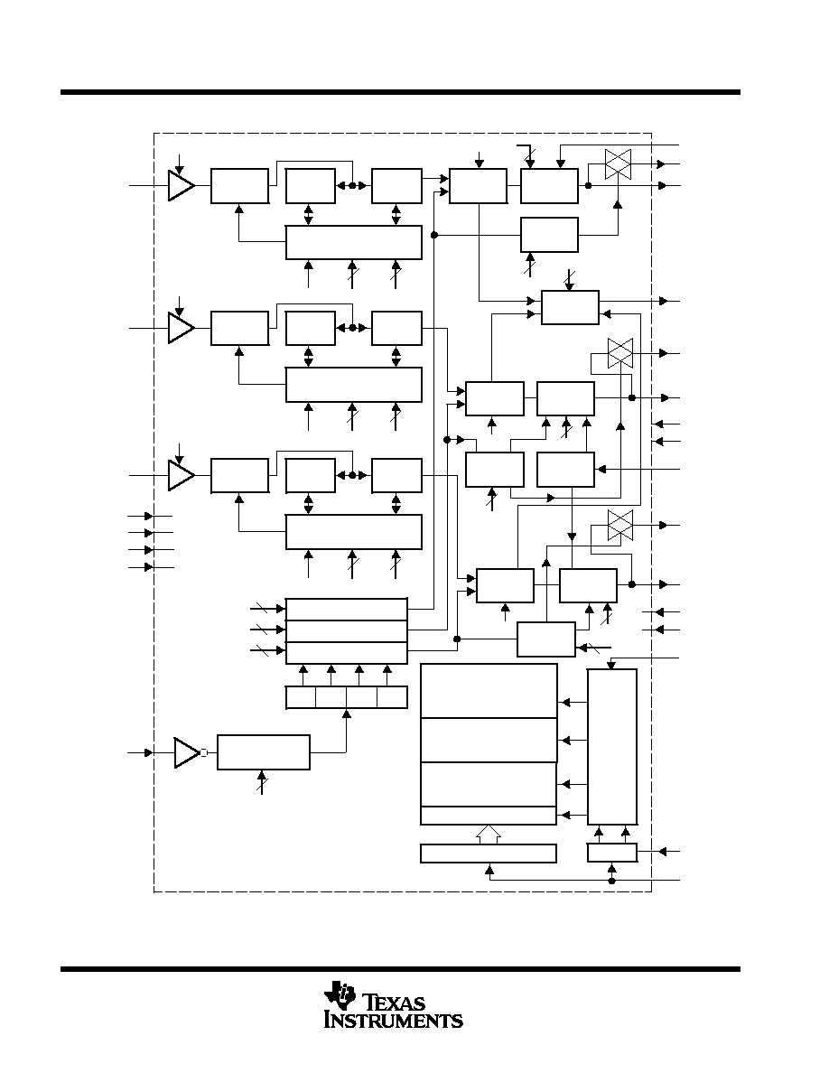
sizer device. The TRF2020 consists of one main
1.2-GHz synthesizer and two auxiliary 250-MHz
synthesizers. Each synthesizer has an independent dual-modulus prescaler and separate powerdown modes.
These features provide maximum flexibility for the design of 900-MHz wireless systems.
The main synthesizer consists of a 32/33-modulus prescaler with an 11-bit counter, a phase-frequency detector,
and a charge pump. The phase-frequency detector is referenced to an internal reference frequency that is
derived from an external TCXO signal. The phase-frequency detector is also provided with a dead-zone
compensation circuit that reduces synthesizer phase noise during locked conditions.
Each auxiliary synthesizer consists of an independent 8/9-modulus prescaler with an 11-bit counter, a
phase-frequency detector, and a charge pump. Similar to the main synthesizer, each auxiliary synthesizer's
phase-frequency detector is referenced to an internal reference frequency that is derived from an external
TCXO signal.
The external TCXO signal is prescaled by an 11-bit counter and then distributed to three independent
postscalers. Each postscaler provides a selectable, divide-by-1, -2, -4, or -8 function before the reference signal
is distributed to the associated synthesizer phase detector. The reference frequency prescaler and independent
postscalers are software programmable.
To achieve minimum lock-up time, each synthesizer contains a speed-up mode charge pump capable of
providing 2 mA output current and an analog switch that can change the loop-filter time constant. The duration
of the speed-up mode operations can be independently controlled with software.
The states of the three internal lock detectors are provided on a programmable, combinational logic output; each
synthesizer can be selected independently or ANDed together.
The device is programmed over a three- wire, synchronous, serial data bus (clock, data, strobe) with achievable
bit rates as high as 20 Mbits/sec. The data is partitioned into words in such a manner that static parameters may
be sent once during initialization, and dynamic parameters, such as frequency, may be sent as often as needed.
The TRF2020 is offered in a 24-pin plastic thin-shrink small-outline package (TSSOP) and is characterized for
free-air operation from 40
°
C to 85
°
C.
These devices have limited built-in ESD protection. The leads should be shorted together or the device placed in conductive foam
during storage or handling to prevent electrostatic damage to the MOS gates.
Copyright
©
1998, Texas Instruments Incorporated
PRODUCTION DATA information is current as of publication date.
Products conform to specifications per the terms of Texas Instruments
standard warranty. Production processing does not necessarily include
testing of all parameters.
Please be aware that an important notice concerning availability, standard warranty, and use in critical applications of
Texas Instruments semiconductor products and disclaimers thereto appears at the end of this data sheet.
TI is a trademark of Texas Instruments Incorporated.
1
2
3
4
5
6
7
8
9
10
11
12
24
23
22
21
20
19
18
17
16
15
14
13
V
DD
CLOCK
DATA
STROBE
LD
V
SS
REF_IN
V
SSP
PDA2
SW2
V
DDP2
AUX2_IN
AUX1_IN
V
DDP1
PDA1
SW1
RPA
V
DDA
SWM
PDM
V
SSA
RPM
V
DDPM
RF_IN
PW PACKAGE
(TOP VIEW)
TRF2020
SYNTHESIZER FOR GLOBAL SYSTEM
FOR MOBILE (GSM) CELLULAR TELEPHONES
SLWS020B FEBRUARY 1995 REVISED JANUARY 1998
2
POST OFFICE BOX 655303
·
DALLAS, TEXAS 75265
functional block diagram
1/32, 33
Prescaler
5-Bit
Counter
11-Bit
Counter
Phase
Detector
Charge
Pump
F
R
Control Logic
2
5
11
Speed-Up
Counter
6
C
R
R
A
B
1/8, 9
Prescaler
3-Bit
Counter
11-Bit
Counter
Control Logic
3
11
S
S
D
E
Phase
Detector
Charge
Pump
Lock
Detect
2
U
S
2
Speed-Up
Counter
Current
Reference
1/8, 9
Prescaler
3-Bit
Counter
11-Bit
Counter
Control Logic
3
11
T
T
H
J
Phase
Detector
Charge
Pump
6
G
Speed-Up
Counter
T
6
G
Main Reference Select
AUX-1 Reference Select
AUX-2 Reference Select
2
2
2
L
M
N
÷
1
÷
2
÷
4
÷
8
11-Bit Reference
Counter
K
11
P
Reference Counter
Power Enable
Lock Detect Select
Test Mode
AUX-2 Synthesizer
Reference Postscaler Select
Auxiliary Current Ratio
AUX-1 Synthesizer
Auxiliary Speed-Up
Main Current Ratio
Main Synthesizer
22-Bit Shift Register
Address
Decoder
Word-3
Word-2
Word-1
Word-0
2 Bit
RPM
SWM
PDM
LD
SW1
PDA1
VSSA
VDDA
RPA
SW2
PDA2
VDD
VSS
STROBE
DATA
CLOCK
RF_IN
AUX1_IN
AUX2_IN
VDDPM
VDDP1
VDDP2
VSSP
REF_IN
13
24
12
14
23
11
8
7
15
18
17
5
21
22
19
16
20
10
9
1
6
4
3
2
2
K
TRF2020
SYNTHESIZER FOR GLOBAL SYSTEM
FOR MOBILE (GSM) CELLULAR TELEPHONES
SLWS020B FEBRUARY 1995 REVISED JANUARY 1998
3
POST OFFICE BOX 655303
·
DALLAS, TEXAS 75265
Terminal Functions
TERMINAL
I/O
DESCRIPTION
NAME
NO.
I/O
DESCRIPTION
AUX1_IN
24
I
RF input auxiliary-1 synthesizer
AUX2_IN
12
I
RF input auxiliary-2 synthesizer
CLOCK
2
I
Clock input
DATA
3
I
Data input
LD
5
O
Lock detect output
PDA1
22
O
Auxiliary-1 synthesizer phase detector output
PDA2
9
O
Auxiliary-2 synthesizer phase detector output
PDM
17
O
Main synthesizer phase detector output
REF_IN
7
I
Reference input
RF_IN
13
I
Main synthesizer RF input
RPA
20
I
Reference current input for AUX-1 and AUX-2 charge pumps
RPM
15
I
Reference current input for main charge pump
STROBE
4
I
Strobe input
SWM
18
O
Main analog switch output
SW1
21
O
Auxiliary-1 analog switch output
SW2
10
O
Auxiliary-2 analog switch output
VDD
1
Digital supply voltage
VDDA
19
Analog supply voltage
VDDPM
14
Main prescaler supply voltage
VDDP1
23
Auxiliary-1 prescaler supply voltage
VDDP2
11
Auxiliary-2 prescaler supply voltage
VSS
6
Digital ground
VSSA
16
Analog ground
VSSP
8
Prescaler ground
absolute maximum ratings over operating free-air temperature (unless otherwise noted)
Supply voltage V
DDP
0.3 V to 4.6 V
. . . . . . . . . . . . . . . . . . . . . . . . . . . . . . . . . . . . . . . . . . . . . . . . . . . . . . . . . . . . . .
Supply voltage V
DD,
V
DDA
0.3 V to 6 V
. . . . . . . . . . . . . . . . . . . . . . . . . . . . . . . . . . . . . . . . . . . . . . . . . . . . . . . . . .
Voltage applied to any other pin, V
IN
0.3 V to V
DD
+ 0.3 V
. . . . . . . . . . . . . . . . . . . . . . . . . . . . . . . . . . . . . . . . .
Power dissipation at or below T
A
= 25
°
C 300
mW
. . . . . . . . . . . . . . . . . . . . . . . . . . . . . . . . . . . . . . . . . . . . . . . . . . .
Junction temperature, T
J
150
°
C
. . . . . . . . . . . . . . . . . . . . . . . . . . . . . . . . . . . . . . . . . . . . . . . . . . . . . . . . . . . . . . . . . .
Ambient operating temperature, T
A
40
°
C to 85
°
C
. . . . . . . . . . . . . . . . . . . . . . . . . . . . . . . . . . . . . . . . . . . . . . . . . .
Storage temperature, T
STG
65
°
C to 150
°
C
. . . . . . . . . . . . . . . . . . . . . . . . . . . . . . . . . . . . . . . . . . . . . . . . . . . . . . .
Stresses beyond those listed under "absolute maximum ratings" may cause permanent damage to the device. These are stress ratings only, and
functional operation of the device at these or any other conditions beyond those indicated under "recommended operating conditions" is not
implied. Exposure to absolute-maximum-rated conditions for extended periods may affect device reliability.
recommended operating conditions
MIN
NOM
MAX
UNIT
VDDA
Analog supply voltage
2.75
3
4.5
V
VDD, VDDP
Digital supply voltage
2.75
3
3.6
V
TA
Operating free-air temperature
40
25
85
°
C
TJ
Junction temperature
30
105
°
C
TRF2020
SYNTHESIZER FOR GLOBAL SYSTEM
FOR MOBILE (GSM) CELLULAR TELEPHONES
SLWS020B FEBRUARY 1995 REVISED JANUARY 1998
4
POST OFFICE BOX 655303
·
DALLAS, TEXAS 75265
electrical characteristics with V
DDA
= 4.5 V, V
DDP
= V
DD
= 3 V, T
A
= 25
°
C (unless otherwise noted)
PARAMETER
TEST CONDITIONS
MIN
TYP
MAX
UNIT
IOPER
Operational supply current
R = S = T = 1
(see Note 1)
11
13
mA
ISTDBY
Maximum standby current
R = S = T = 0
10
µ
A
IDDPM
Main synthesizer operational supply current
R = 1, S = T = 0
(see Note 1)
6
8
mA
IDDP1
Auxiliary-1 synthesizer operational supply current
R = 0, S = 1, T = 0 (see Note 1)
3.3
4.5
mA
IDDP2
Auxiliary-2 synthesizer operational supply current
R = 0, S = 0, T = 1 (see Note 1)
3.3
4.5
mA
NOTES:
1. Operational supply currents measured with RF_IN = 1200 MHz, AUX1_IN = 250 MHz, AUX2_IN = 250 MHz, fREF_IN = 39.6 MHz.
All loops are in lock condition and normal mode. Operational supply current = IOPER = IDDA + IDDP1 + IDDP2 + IDDPM + IDD
digital interface characteristics
PARAMETER
TEST CONDITIONS
MIN
TYP
MAX
UNIT
Clock
VIH
High-level input voltage
Data
0.7 VDD
VDD
V
Strobe
Clock
VIL
Low-level input voltage
Data
0
0.3 VDD
V
Strobe
Clock
IIH
High-level input current
Data
0
1
µ
A
Strobe
Clock
IIL
Low-level input current
Data
0
1
µ
A
Strobe
VOH
High-level output voltage
LD
IOH = 1 mA
VDD 0.4
V
VOL
Low-level output voltage
LD
IOH = 2 mA
0.4
V
ac electrical characteristics with V
DDA
= 4.5 V, V
DDP
= V
DD
= 3 V, T
A
= 25
°
C (unless otherwise noted)
main loop, RF_IN
PARAMETER
TEST CONDITIONS
MIN
TYP
MAX
UNIT
fRF_IN
Input signal frequency
2.75
VDDP
3.5 V
1200
MHz
PRF_IN
Input sensitivity
2.75
VDDP
3.5 V,
Rsource = 50
20
0
dBm
fCOMP
Phase detector comparison
2.75
VDD
3.5 V
0
2
MHz
auxiliary loops, AUX1_IN and AUX2_IN
PARAMETER
TEST CONDITIONS
MIN
TYP
MAX
UNIT
fAUX_IN Input signal frequency
2.75
VDDP
3.5 V
250
MHz
PAUX_IN Input sensitivity
2.75
VDDP
3.5 V,
Rsource = 50
20
0
dBm
fAUX_
COMP
Phase detector comparison
2.75
VDD
3.5 V
0
2
MHz
TRF2020
SYNTHESIZER FOR GLOBAL SYSTEM
FOR MOBILE (GSM) CELLULAR TELEPHONES
SLWS020B FEBRUARY 1995 REVISED JANUARY 1998
5
POST OFFICE BOX 655303
·
DALLAS, TEXAS 75265
reference divider, REF_IN
PARAMETER
TEST CONDITIONS
MIN
TYP
MAX
UNIT
fREF_IN
Input signal frequency
2.75
VDDP
3.5 V
40
MHz
VREF_IN
Input sensitivity
0.3
VDDP 0.8
Vpp
ZREF IN
Input impedance
Resistive
100
k
ZREF_IN
Input impedance
Capacitive
3
pF
charge pump characteristics
main charge pump output
ÁÁÁÁÁÁÁÁÁÁÁÁÁÁÁÁ
ÁÁÁÁÁÁÁÁÁÁÁÁÁÁÁÁ
PARAMETER
TEST CONDITIONS
MIN
ÁÁÁ
ÁÁÁ
TYP
ÁÁÁ
ÁÁÁ
MAX
ÁÁÁ
ÁÁÁ
UNIT
ÁÁÁÁ
ÁÁÁÁ
|IPDM|
ÁÁÁÁÁÁÁÁÁ
ÁÁÁÁÁÁÁÁÁ
Output current PDM
normal mode
VPDM = 0 5 VDDA
400
ÁÁÁ
ÁÁÁ
500
ÁÁÁ
ÁÁÁ
600
ÁÁÁ
ÁÁÁ
µ
A
ÁÁÁÁ
ÁÁÁÁ
|IPDM|
ÁÁÁÁÁÁÁÁÁ
ÁÁÁÁÁÁÁÁÁ
Output current PDM
speed-up mode
VPDM = 0.5 VDDA
1.5
ÁÁÁ
ÁÁÁ
2
ÁÁÁ
ÁÁÁ
2.5
ÁÁÁ
ÁÁÁ
mA
ÁÁÁÁ
ÁÁÁÁ
D
I
PDM
|I
PDM
|
ÁÁÁÁÁÁÁÁÁÁÁÁÁ
ÁÁÁÁÁÁÁÁÁÁÁÁÁ
Relative output current variation PDM (see Figure 1)
RPM 5% tolerance,
VSSA + 0.5
VPDM
VDDA 0.5
ÁÁÁ
ÁÁÁ
ÁÁÁ
ÁÁÁ
15
ÁÁÁ
ÁÁÁ
%
ÁÁÁÁ
ÁÁÁÁ
IPDM
ÁÁÁÁÁÁÁÁÁÁÁÁÁ
ÁÁÁÁÁÁÁÁÁÁÁÁÁ
Output current matching (see Figure 1)
VPDM = 0.5 VDDA
ÁÁÁ
ÁÁÁ
ÁÁÁ
ÁÁÁ
ÁÁÁ
ÁÁÁ
8
ÁÁÁ
ÁÁÁ
%
ÁÁÁÁ
ÁÁÁÁ
|ISWM|
ÁÁÁÁÁÁÁÁÁÁÁÁÁ
ÁÁÁÁÁÁÁÁÁÁÁÁÁ
Analog switch output current SWM, speed-up mode
VSWM = 0.5 VDDA
1.5
ÁÁÁ
ÁÁÁ
2
ÁÁÁ
ÁÁÁ
2.5
ÁÁÁ
ÁÁÁ
mA
RPM = RPA = 27 k
to VSSA, F = K = 10.
auxiliary-1 charge pump output
ÁÁÁÁÁÁÁÁÁÁÁÁÁÁÁÁ
ÁÁÁÁÁÁÁÁÁÁÁÁÁÁÁÁ
PARAMETER
TEST CONDITIONS
MIN
ÁÁÁ
ÁÁÁ
TYP
ÁÁÁ
ÁÁÁ
MAX
ÁÁÁ
ÁÁÁ
UNIT
ÁÁÁÁ
ÁÁÁÁ
|IPDA1|
ÁÁÁÁÁÁÁÁÁ
ÁÁÁÁÁÁÁÁÁ
Output current PDA1
normal mode
VPDA1 = 0 5 VDDA
400
ÁÁÁ
ÁÁÁ
500
ÁÁÁ
ÁÁÁ
600
ÁÁÁ
ÁÁÁ
µ
A
ÁÁÁÁ
ÁÁÁÁ
|IPDA1|
ÁÁÁÁÁÁÁÁÁ
ÁÁÁÁÁÁÁÁÁ
Output current PDA1
speed-up mode
VPDA1 = 0.5 VDDA
1.5
ÁÁÁ
ÁÁÁ
2
ÁÁÁ
ÁÁÁ
2.5
ÁÁÁ
ÁÁÁ
mA
ÁÁÁÁ
Á
ÁÁ
Á
ÁÁÁÁ
D
I
PDA1
|I
PDA1
|
ÁÁÁÁÁÁÁÁÁÁÁÁÁ
Á
ÁÁÁÁÁÁÁÁÁÁÁ
Á
ÁÁÁÁÁÁÁÁÁÁÁÁÁ
Relative output current variation PDA1
(see Figure 1)
RPA 5% tolerance
VSSA + 0.5
VPDA1
VDDA 0.5
ÁÁÁ
Á
Á
Á
ÁÁÁ
ÁÁÁ
Á
Á
Á
ÁÁÁ
15
ÁÁÁ
Á
Á
Á
ÁÁÁ
%
ÁÁÁÁ
ÁÁÁÁ
IPDA1
ÁÁÁÁÁÁÁÁÁÁÁÁÁ
ÁÁÁÁÁÁÁÁÁÁÁÁÁ
Output current matching (see Figure 1)
VPDA1 = 0.5 VDDA
ÁÁÁ
ÁÁÁ
ÁÁÁ
ÁÁÁ
ÁÁÁ
ÁÁÁ
8
ÁÁÁ
ÁÁÁ
%
ÁÁÁÁ
ÁÁÁÁ
|ISW1|
ÁÁÁÁÁÁÁÁÁÁÁÁÁ
ÁÁÁÁÁÁÁÁÁÁÁÁÁ
Analog switch output current SW1, speed-up mode
VSW1 = 0.5 VDDA
1.5
ÁÁÁ
ÁÁÁ
2
ÁÁÁ
ÁÁÁ
2.5
ÁÁÁ
ÁÁÁ
mA
RPM = RPA = 27 k
to VSSA, F = K = 10.
auxiliary-2 charge pump output
ÁÁÁÁÁÁÁÁÁÁÁÁÁÁÁÁ
ÁÁÁÁÁÁÁÁÁÁÁÁÁÁÁÁ
PARAMETER
TEST CONDITIONS
MIN
ÁÁÁ
ÁÁÁ
TYP
ÁÁÁ
ÁÁÁ
MAX
ÁÁÁ
ÁÁÁ
UNIT
ÁÁÁÁ
ÁÁÁÁ
|IPDA2|
ÁÁÁÁÁÁÁÁÁ
ÁÁÁÁÁÁÁÁÁ
Output current PDA2
normal mode
VPDA2 = 0 5 VDDA
400
ÁÁÁ
ÁÁÁ
500
ÁÁÁ
ÁÁÁ
600
ÁÁÁ
ÁÁÁ
µ
A
ÁÁÁÁ
|IPDA2|
ÁÁÁÁÁÁÁÁÁ
Output current PDA2
speed-up mode
VPDA2 = 0.5 VDDA
1.5
ÁÁÁ
2
ÁÁÁ
2.5
ÁÁÁ
mA
ÁÁÁÁ
Á
ÁÁ
Á
ÁÁÁÁ
D
I
PDA2
|I
PDA2
|
ÁÁÁÁÁÁÁÁÁÁÁÁÁ
Á
ÁÁÁÁÁÁÁÁÁÁÁ
Á
ÁÁÁÁÁÁÁÁÁÁÁÁÁ
Relative output current variation PDA2
(see Figure 1)
RPA 5% tolerance
VSSA + 0.5
VPDA2
VDDA 0.5
ÁÁÁ
Á
Á
Á
ÁÁÁ
ÁÁÁ
Á
Á
Á
ÁÁÁ
15
ÁÁÁ
Á
Á
Á
ÁÁÁ
%
ÁÁÁÁ
ÁÁÁÁ
IPDA2
ÁÁÁÁÁÁÁÁÁÁÁÁÁ
ÁÁÁÁÁÁÁÁÁÁÁÁÁ
Output current matching (see Figure 1)
VPDA2 = 0.5 VDDA
ÁÁÁ
ÁÁÁ
ÁÁÁ
ÁÁÁ
ÁÁÁ
ÁÁÁ
8
ÁÁÁ
ÁÁÁ
%
ÁÁÁÁ
ÁÁÁÁ
|ISW2|
ÁÁÁÁÁÁÁÁÁÁÁÁÁ
ÁÁÁÁÁÁÁÁÁÁÁÁÁ
Analog switch output current SW2, speed-up mode
VSW2 = 0.5 VDDA
1.5
ÁÁÁ
ÁÁÁ
2
ÁÁÁ
ÁÁÁ
2.5
ÁÁÁ
ÁÁÁ
mA
RPM = RPA = 27 k
to VSSA, F = K = 10.
TRF2020
SYNTHESIZER FOR GLOBAL SYSTEM
FOR MOBILE (GSM) CELLULAR TELEPHONES
SLWS020B FEBRUARY 1995 REVISED JANUARY 1998
6
POST OFFICE BOX 655303
·
DALLAS, TEXAS 75265
I2
I1
I2
I1
Current
Voltage
IOUT REL
IOUT MATCH
ISINK
ISOURCE
IOUT REL
V1
V2
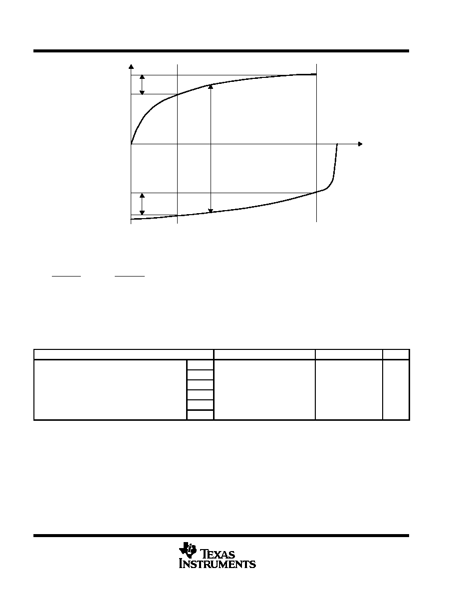
Figure 1. Charge-Pump Output Current Definitions
The relative output current variation is defined as the percent difference between charge-pump current output
at two charge-pump output voltages and the mean charge-pump current output:
D
I
OUT REL
I
OUT MEAN
+
2
(I
2
I
1
)
|(I
2
)
I
1
)|
x 100%; with V
1
= 0.5 V, V
2
= V
DDA
0.5 V.
Output current matching is defined as the difference in charge-pump sinking current output and charge-pump
sourcing current output at a given charge-pump output (see Figure 1).
I
OUT MATCH
= I
SINK
I
SOURCE
; with V
1
Voltage
V
2
.
charge-pump leakage currents, charge pumps not active
PARAMETER
TEST CONDITIONS
MIN
TYP
MAX
UNIT
PDM
PDA1
IOZ
Disabled output current
PDA2
VO = 0.5VDDA,
RPM = RPA = VDDA
10
nA
IOZ
Disabled output current
SWM
RPM = RPA = VDDA,
Normal and speed-up modes
10
nA
SW1
Normal and s eed u modes
SW2
TRF2020
SYNTHESIZER FOR GLOBAL SYSTEM
FOR MOBILE (GSM) CELLULAR TELEPHONES
SLWS020B FEBRUARY 1995 REVISED JANUARY 1998
7
POST OFFICE BOX 655303
·
DALLAS, TEXAS 75265
serial interface timing requirements with
V
DDA
= 4.5 V, V
DDP
= V
DD
= 3.0 V, T
A
= 25
°
C
PARAMETER
TEST CONDITIONS
MIN
TYP
MAX
UNIT
CI
Input capacitance
10
pF
RI
Input resistance
10 k
fclock
CLOCK frequency
13
20
MHz
tr, tf
CLOCK input rise and fall time
8
ns
tw(High)
Pulse duration, CLOCK high
20
ns
tw(Low)
Pulse duration, CLOCK low
20
ns
Data before CLOCK high
15
ns
tsu
Under continuous operation
15
ns
tsu
Strobe before CLOCK high
First power on or programmed
from standby mode
10
Cext_coupling
60 k
µ
s
th
Data after CLOCK high
15
ns
th
Strobe after CLOCK high
15
ns
tw(pulse)
Strobe pulse width
2
REF_IN
s
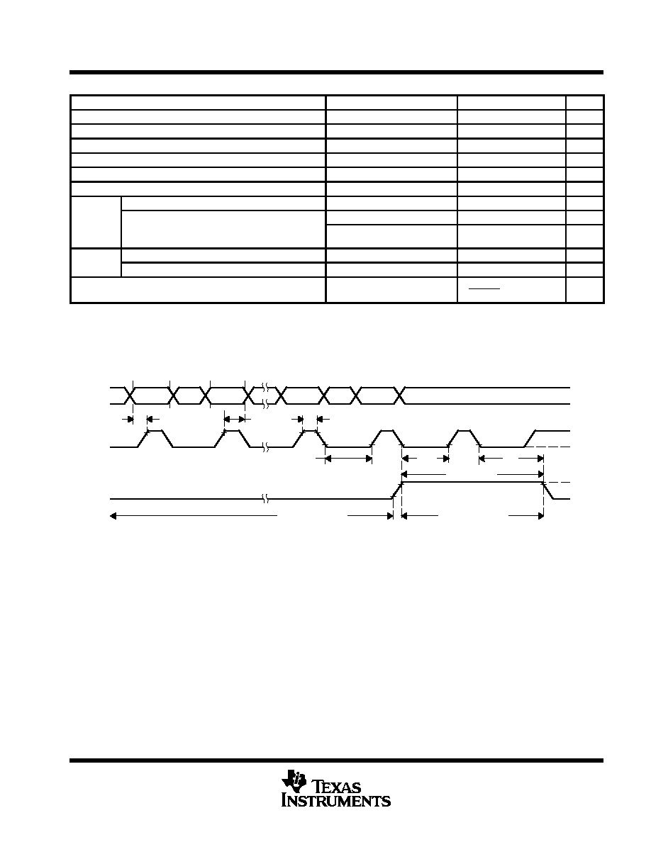
PARAMETER MEASUREMENT INFORMATION
The timing relationship between the TRF2020 Data, Clock, and Strobe registers is shown in Figure 2.
D0
D1
D22
D23
tsu
th
tw(HIGH)
tw(LOW)
tsu
th
tw(PULSE)
Clock Disabled
Store Data
Clock Enabled
Shift in Data
Data
Valid
Data
Change
DATA
CLOCK
STROBE
VIH
VIL
VIH
VIL
VIH
VIL
Figure 2. Serial Data Interface Timing

TRF2020
SYNTHESIZER FOR GLOBAL SYSTEM
FOR MOBILE (GSM) CELLULAR TELEPHONES
SLWS020B FEBRUARY 1995 REVISED JANUARY 1998
8
POST OFFICE BOX 655303
·
DALLAS, TEXAS 75265
TYPICAL CHARACTERISTICS
Figure 3
f Frequency MHz
50
40
30
20
10
0
MAIN DIVIDER INPUT POWER
vs.
FREQUENCY AND SUPPLY VOLTAGE
IP
Input Power dBm
3.5 V
2.75 V
TA = 25
°
C
500
600
700
800
900
1000
1
100
1200
1300
1400
1500
1600
1700
1800
1900
2000
Figure 4
50
40
30
20
10
MAIN DIVIDER MINIMUM INPUT POWER
vs.
FREQUENCY AND TEMPERATURE
MIP
Minimum Input Power dBm
VDDA = VDDP = VDD = 2.75 V
TA = 40
°
C
TA = 25
°
C
TA = 85
°
C
f Frequency MHz
500
600
700
800
900
1000
1
100
1200
1300
1400
1500
1600
1700
1800
1900
2000
0
Figure 5
40
38
36
0.02
f Frequency MHz
0
0.04
0.06
0.08
0.1
0.12
34
32
30
28
26
24
22
20
18
16
14
12
10
8
6
4
REFERENCE DIVIDER MINIMUM INPUT VOLTAGE
vs.
FREQUENCY AND SUPPLY VOLTAGE
MIV Minimum Input V
oltage V
PP
3.5 V
2.75 V
TA = 25
°
C
Figure 6
40
38
36
0.02
f Frequency MHz
0
0.04
0.06
0.08
0.1
0.12
34
32
30
28
26
24
22
20
18
16
14
12
10
8
6
4
REFERENCE DIVIDER MINIMUM INPUT VOLTAGE
vs.
FREQUENCY AND TEMPERATURE
MIV Minimum Input V
oltage V
PP
VDDA = VDDP = VDD = 2.75 V
TA = 40
°
C
TA = 25
°
C
TA = 85
°
C
TRF2020
SYNTHESIZER FOR GLOBAL SYSTEM
FOR MOBILE (GSM) CELLULAR TELEPHONES
SLWS020B FEBRUARY 1995 REVISED JANUARY 1998
9
POST OFFICE BOX 655303
·
DALLAS, TEXAS 75265
TYPICAL CHARACTERISTICS
Figure 7
35
500
450
25
f Frequency MHz
30
20
15
10
5
0
400
350
300
250
200
150
100
50
AUXILIARY-1 DIVIDER MINIMUM INPUT POWER
vs.
FREQUENCY AND SUPPLY VOLTAGE
MIP
Minimum Input Power dBm
TA = 25
°
C
3.5 V
2.75 V
Figure 8
35
500
450
25
f Frequency MHz
30
20
15
10
5
0
400
350
300
250
200
150
100
50
AUXILIARY-1 DIVIDER MINIMUM INPUT POWER
vs.
FREQUENCY AND TEMPERATURE
MIP
Minimum Input Power dBm
TA = 40
°
C
TA = 25
°
C
TA = 85
°
C
VDDA = VDDP = VDD = 2.75 V
Figure 9
40
35
500
450
25
f Frequency MHz
30
20
15
10
5
0
400
350
300
250
200
150
100
50
AUXILIARY-2 DIVIDER MINIMUM INPUT POWER
vs.
FREQUENCY AND SUPPLY VOLTAGE
MIP
Minimum Input Power dBm
3.5 V
2.75 V
TA = 25
°
C
Figure 10
40
35
500
450
25
f Frequency MHz
30
20
15
10
5
0
400
350
300
250
200
150
100
50
AUXILIARY-2 DIVIDER MINIMUM INPUT POWER
vs.
FREQUENCY AND SUPPLY VOLTAGE
MIP
Minimum Input Power dBm
VDDA = VDDP = VDD = 2.75 V
TA = 40
°
C
TA = 25
°
C
TA = 85
°
C
TRF2020
SYNTHESIZER FOR GLOBAL SYSTEM
FOR MOBILE (GSM) CELLULAR TELEPHONES
SLWS020B FEBRUARY 1995 REVISED JANUARY 1998
10
POST OFFICE BOX 655303
·
DALLAS, TEXAS 75265
TYPICAL CHARACTERISTICS
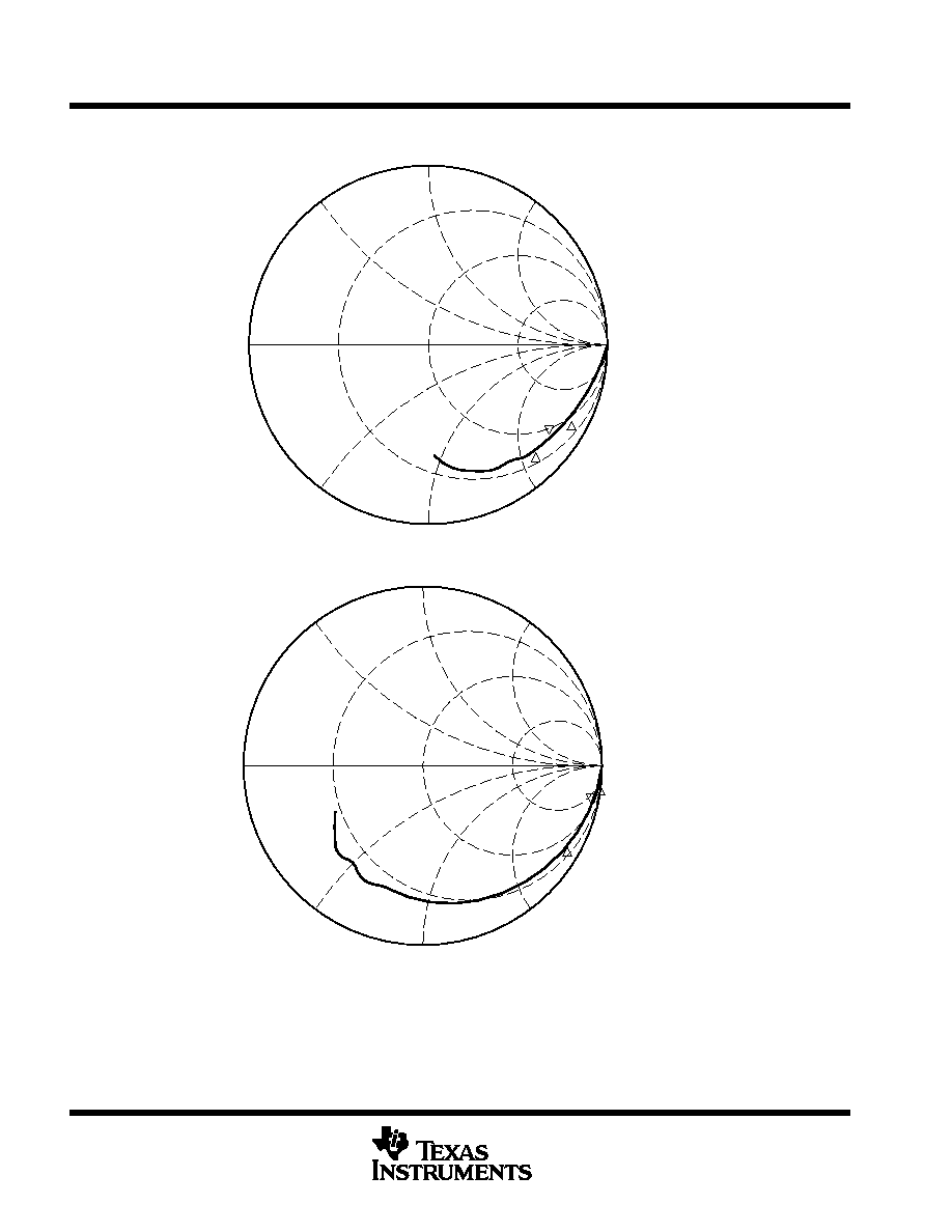
CH1
S11 1 U FS
START
.030 000 MHz
STOP 2 000.000 000 MHz
1: 34.688
133.84
1.1 GHz
2: 29.848
116.08
1.2 GHz
3: 45.211
182.11
900 MHz
1
2
3
Figure 11. Typical RF_IN Input Impedance (S
11
)
CH1
S11 1 U FS
START
.030 000 MHz
STOP 2 000.000 000 MHz
1: 58.672
403.83
250 MHz
2: 33.328
189.11
500 MHz
3: 109.47
1,0037 k
100 MHz
1
2
3
Figure 12. Typical AUX1_IN Input Impedance (S
11
)

TRF2020
SYNTHESIZER FOR GLOBAL SYSTEM
FOR MOBILE (GSM) CELLULAR TELEPHONES
SLWS020B FEBRUARY 1995 REVISED JANUARY 1998
11
POST OFFICE BOX 655303
·
DALLAS, TEXAS 75265
CH1
S11 1 U FS
START
.030 000 MHz
STOP 2 000.000 000 MHz
1: 57.031
398.92
250 MHz
2: 32.273
188.6
500 MHz
3: 107.63
982.31
100 MHz
1
2
3
Figure 13. Typical AUX2_IN Input Impedance (S
11
)
CH1
S11 1 U FS
START
.030 000 MHz
STOP 2 000.000 000 MHz
1: 803.75
4.9245
16.8 MHz
2: 218.88
2.148 k
40 MHz
3: 601
4.1308
20.0 MHz
1
2
3
Figure 14. Typical REF_IN Input Impedance (S
11
)
TRF2020
SYNTHESIZER FOR GLOBAL SYSTEM
FOR MOBILE (GSM) CELLULAR TELEPHONES
SLWS020B FEBRUARY 1995 REVISED JANUARY 1998
12
POST OFFICE BOX 655303
·
DALLAS, TEXAS 75265
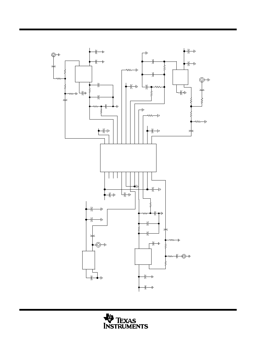
APPLICATION INFORMATION
Figure 15. Evaluation Board Schematic (Part 1 of 2)
VCONT
GND
VCC
OUT
3
2
14
J4
VOSC2
NDKOSC
REFIN
C60
22 pF
C62
1000 pF
C22
R49
18
R46
50
C48
220 pF
VOSC1
AUX2_VCO
VCO190S V
ARIL
VT
MOD
VCC
RF_OUT
14
10
2
6
C52
0.1
µ
F
C55
33 pF
C57
330 pF
R56
51 k
C58
12 nF
R59
15 k
R54
12 k
R50
18
R47
18
J3
C45
220pF
C64
22 pF
C51
0.1
µ
F
C14
47 pF
R17
33 k
C13
820 pF
C19
4700 pF
R21
20 k
R24
18
R26
18
J2
R23
18
R25
50
C20
R18
C43
220pF
C12
VOSC1
AUX1_VCO
VCO190S V
ARIL
12 k
VT
MOD
VCC
RF_OUT
14
10
2
6
0.1
µ
F
C24
220 pF
C59
22 pF
0.1
µ
F
C41
0.1
µ
F
R43
24 k
V
DDA
C42
0.1
µ
F
V
DD
C44
0.1
µ
F
R9
24 k
OUT
R12
18
VOSC2
VT
MOD
5
1
3
7
VCC
RF_OUT
MVCO
VCO191U V
ARIL
C16
68 pF
C18
680pF
R22
18 k
C6
4700 pF
R20
12 k
C7
0.1
µ
C61
F
0.1
µ
F
C63
22 pF
R15
18
C46
100 pF
J1
R1
1
18
R10
50
C8
100 pF
24
23
22
21
20
19
18
17
16
15
14
13
AUX_IN
VDDP1
PDA1
SW1
RP
A
VDDA
SWM
PDM
VSSA
RPM
VDDPM
RF_IN
TRF2020
U1
VDD
CLOCK
DA
T
A
STROBE
LD
VSS
REF_IN
VSSP
PDA2
SW2
VDDP2
AUX2_IN
1
2
3
4
5
6
7
8
9
10
11
12
C40
0.1
µ
F
C15
DNP
C39
0.1
µ
F
VDD
C23
22 nF
TCXO
VDD
R19
36 k
0.1
µ
F

TRF2020
SYNTHESIZER FOR GLOBAL SYSTEM
FOR MOBILE (GSM) CELLULAR TELEPHONES
SLWS020B FEBRUARY 1995 REVISED JANUARY 1998
13
POST OFFICE BOX 655303
·
DALLAS, TEXAS 75265
APPLICATION INFORMATION
VT
VO
NC
VO
5
2
1
7
3
6
VO
VO
LM317LBD
VR5
A
NC
4
8
VOPTO
R37
270
+
C25
µ
1
F
R38
820
VT
VO
NC
VO
5
2
1
7
3
6
VO
VO
LM317LBD
VR4
A
NC
4
8
VOSC2
R13
270
+
C5
µ
1
F
R8
390
VT
VO
NC
VO
5
2
1
7
3
6
VO
VO
LM317LBD
VR3
A
NC
4
8
VOSC1
R3
270
+
R7
820
C4
µ
1
F
VT
VO
NC
VO
5
2
1
7
3
6
VO
VO
LM317LBD
VR2
A
NC
4
8
VDD
R2
220
+
R6
C3
µ
1
F
1 k
CW
CCW
W
VDD
VT
VO
NC
VO
5
2
1
7
3
6
VO
VO
LM317LBD
VR1
A
NC
4
8
VDDA
R1
220
+
R5
C2
µ
1
F
1 k
CW
CCW
W
VDDA
+
C1
µ
4.7
F
AGND
HUB
DGND
GND
POWER
POWER
NOTE: Evaluation board dc supply circuitry
To U1/2
1
9
4
5
6
LOCK
U4
U3
U2
U5
4N28S
4N28S
4N28S
VOPTO
CLOCK1
DATA
STROBE
R27
1.8 k
R31
3.6 k
R28
1.8 k
R32
3.6 k
R29
1.8 k
R33
3.6 k
R30
2.7 k
R34
1.8 k
VDD
FOR PC INTERFACE ONLY
1
14
2
15
3
16
4
17
5
18
6
19
7
20
8
21
9
22
10
23
11
24
12
25
13
CLOCK
DATA1
STROBE1
CLOCK
STROBE
DATA
CLOCK
To U1/5
To U1/4
To U1/3
MOC8030
Figure 15. Evaluation Board Schematic (Part 2 of 2)
TRF2020
SYNTHESIZER FOR GLOBAL SYSTEM
FOR MOBILE (GSM) CELLULAR TELEPHONES
SLWS020B FEBRUARY 1995 REVISED JANUARY 1998
14
POST OFFICE BOX 655303
·
DALLAS, TEXAS 75265
APPLICATION INFORMATION
Table 1. TRF2020 Evaluation Board Parts List
DESIGNATORS
DESCRIPTION
VALUE
QTY
SIZE
(mm)
MANUFACTURER
MANUFACTURER
P/N
C1
Capacitor
4.7 uF
1
"A" 3.2x1.6
Venkel
TA025TCM series
C2, 3, 4, 5, 25
Capacitor
1 uF
5
"A" 3.2x1.6
Venkel
TA025TCM series
C6, 19
Capacitor
4700 pF
2
0603 1.6x.08
Murata
GRM39X7R series
C7, 12, 20, 22,
39, 40, 41, 42,
44, 51, 52, 61
Capacitor
0.1 uF
12
0603 1.6x.08
Murata
GRM39X7R series
C8, 46
Capacitor
100 pF
2
0603 1.6x.08
Murata
GRM39X7R series
C13
Capacitor
820 pF
1
0603 1.6x.08
Murata
GRM39X7R series
C14
Capacitor
47 pF
1
0603 1.6x.08
Murata
GRM39X7R series
C15
Capacitor
DNP
1
0603 1.6x.08
C16
Capacitor
68 pF
1
0603 1.6x.08
Murata
GRM39X7R series
C18
Capacitor
680 pF
1
0603 1.6x.08
Murata
GRM39X7R series
C23
Capacitor
22 nF
1
0603 1.6x.08
Murata
GRM39X7R series
C24, 43, 45, 48
Capacitor
220 pF
4
0603 1.6x.08
Murata
GRM39X7R series
C55
Capacitor
33 pF
1
0603 1.6x.08
Murata
GRM39X7R series
C57
Capacitor
330 pF
1
0603 1.6x.08
Murata
GRM39X7R series
C58
Capacitor
12 nF
1
0603 1.6x.08
Murata
GRM39X7R series
C59, 60, 63, 64
Capacitor
22 pF
4
0603 1.6x.08
Murata
GRM39X7R series
C62
Capacitor
1000 pF
1
0603 1.6x.08
Murata
GRM39X7R series
R1, 2
Resistor
220
2
0603 1.6x.08
Panasonic
ERJ3GSYJ series
R3, 13, 37
Resistor
270
3
0603 1.6x.08
Panasonic
ERJ3GSYJ series
R5, 6
Resistor
1K
2
.25" square
Bourns
3269W001 series
R7, 38
Resistor
820
2
0603 1.6x.08
Panasonic
ERJ3GSYJ series
R8
Resistor
390
1
0603 1.6x.08
Panasonic
ERJ3GSYJ series
R9, 43
Resistor
24K
2
0603 1.6x.08
Panasonic
ERJ3GSYJ series
R10, 25, 46
Resistor
50
3
0603 1.6x.08
Panasonic
ERJ3GSYJ series
R11, 12, 15, 23,
24, 26, 47, 49, 50
Resistor
18
9
0603 1.6x.08
Panasonic
ERJ3GSYJ series
R17
Resistor
33K
1
0603 1.6x.08
Panasonic
ERJ3GSYJ series
R18, 20, 54
Resistor
12K
3
0603 1.6x.08
Panasonic
ERJ3GSYJ series
R19
Resistor
36K
1
0603 1.6x.08
Panasonic
ERJ3GSYJ series
R21
Resistor
20K
1
0603 1.6x.08
Panasonic
ERJ3GSYJ series
R22
Resistor
18K
1
0603 1.6x.08
Panasonic
ERJ3GSYJ series
R27, 28, 29, 34
Resistor
1.8K
4
0603 1.6x.08
Panasonic
ERJ3GSYJ series
R30
Resistor
2.7K
1
0603 1.6x.08
Panasonic
ERJ3GSYJ series
R31, 32, 33
Resistor
3.6K
3
0603 1.6x.08
Panasonic
ERJ3GSYJ series
R56
Resistor
51K
1
0603 1.6x.08
Panasonic
ERJ3GSYJ series
R59
Resistor
15K
1
0603 1.6x.08
Panasonic
ERJ3GSYJ series
U1
Integrated Circuit
1
TI
TRF2020
U2, 3, 4
Optoelectronics
3
730C04
Motorola
4N28S
TRF2020
SYNTHESIZER FOR GLOBAL SYSTEM
FOR MOBILE (GSM) CELLULAR TELEPHONES
SLWS020B FEBRUARY 1995 REVISED JANUARY 1998
15
POST OFFICE BOX 655303
·
DALLAS, TEXAS 75265
APPLICATION INFORMATION
Table 1. TRF2020 Evaluation Board Parts List (Continued)
DESIGNATORS
DESCRIPTION
VALUE
QTY
SIZE
(mm)
MANUFACTURER
MANUFACTURER
P/N
U5
Optoelectronics
1
730C 04
Motorola
MOC8030S
VR1, 2, 3, 4, 5
Voltage regulator
5
SO 8
National
Semiconductor
LM317LBD
P1
Para. connector
1
AMP
747238 4
J1, 2, 3, 4
SMA connector
4
EF Johnson
142 0701 831
MVCO
Voltage
-
controlled
oscillator
1
Vari
-
L Comp.
VCO190U
TCXO
Temp.
-
compensated
crystal oscillator
1
Toyocom
TCO 980 series
AUX 1_VCO
Voltage
-
controlled
oscillator
1
Vari
-
L Comp.
VCO190S
AUX 2_VCO
Voltage
-
controlled
oscillator
1
Vari
-
L Comp.
VCO190S
DATA, VDDA,
VDD, LOCK,
POWER,
CLOCK, GND,
STROBE
Test point
8
Components Corp.
TP 105 01 series
ATTEN 10 dB
RL 0 dBm
VAVG 50
10 dB/
CENTER 1.1089992 GHz
RBW 3 kHz VBW 3 kHz
SPAN 500 kHz
SWP 140 ms
MKR 85.33 dB
200 kHz
MKR
200 kHz
85.33 dB
D
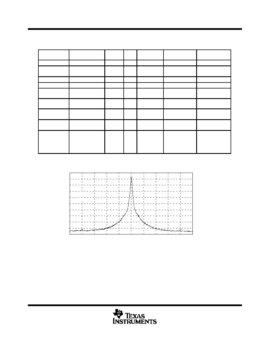
Figure 16. Typical Main Synthesizer Reference Spurs

TRF2020
SYNTHESIZER FOR GLOBAL SYSTEM
FOR MOBILE (GSM) CELLULAR TELEPHONES
SLWS020B FEBRUARY 1995 REVISED JANUARY 1998
16
POST OFFICE BOX 655303
·
DALLAS, TEXAS 75265
APPLICATION INFORMATION
ATTEN 10 dB
RL 0 dBm
VAVG 50
10 dB/
CENTER 1.10899908 GHz
RBW 300 Hz VBW 300 Hz
SPAN 30 kHz
SWP 840 ms
MKR 45.83 dB
4 kHz
MKR
4 kHz
45.83 dB
D
Figure 17. Typical Main Synthesizer Close-in Noise at 4 kHz Offset
ATTEN 10 dB
RL 0 dBm
VAVG 50
10 dB/
CENTER 1.10899918 GHz
RBW 100 Hz VBW 100 Hz
SPAN 10 kHz
SWP 802 ms
MKR 51.50 dB
1 kHz
MKR
1 kHz
51.50 dB
D
Figure 18. Typical Main Synthesizer Close-in Noise at 1 kHz Offset
TRF2020
SYNTHESIZER FOR GLOBAL SYSTEM
FOR MOBILE (GSM) CELLULAR TELEPHONES
SLWS020B FEBRUARY 1995 REVISED JANUARY 1998
17
POST OFFICE BOX 655303
·
DALLAS, TEXAS 75265
APPLICATION INFORMATION
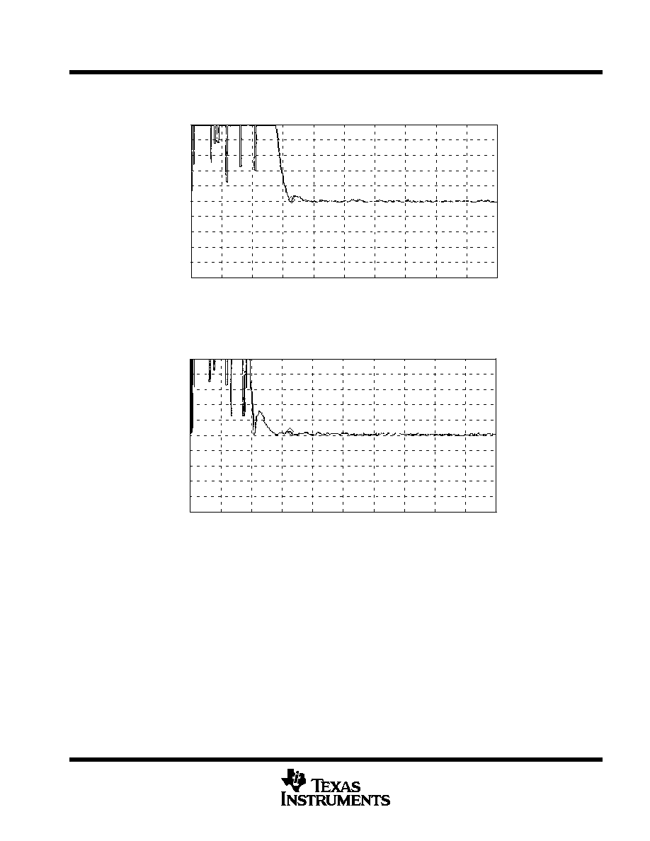
TRACE A: Ch1 FM Main Time
A Marker
652.3438 us
643.05 Hzpk
25
kHzpk
LinMag
5
kHz
/div
25
kHzpk
Start: 0 s
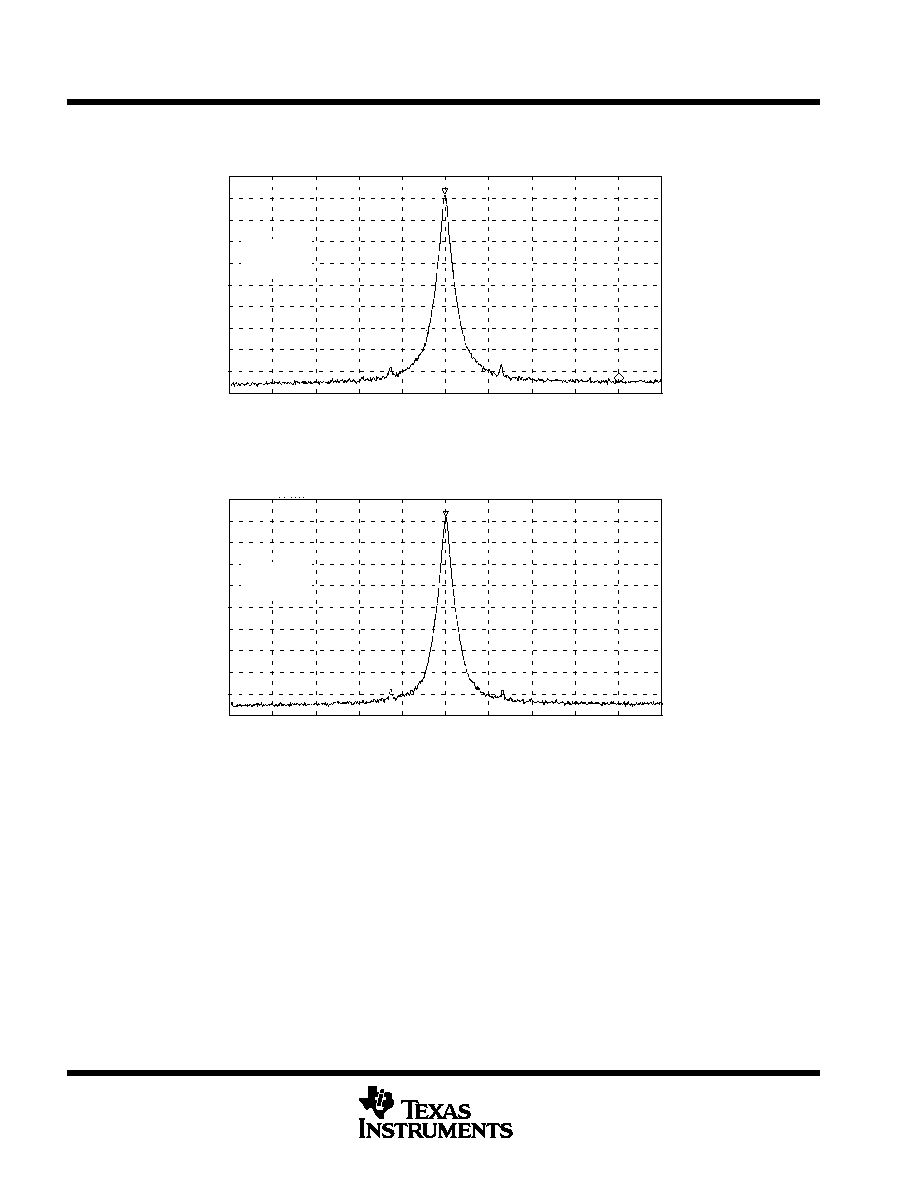
Stop: 1.99609375 ms
Figure 19. Typical Main Synthesizer Transient Response For 35
-
MHz Jump From 1074 MHz to 1109 MHz
TRACE A: Ch1 FM Main Time
A Marker
652.4375 us
893.77 Hzpk
25
kHzpk
LinMag
5
kHz
/div
25
kHzpk
Start: 0 s
Stop: 1.99609375 ms
Figure 20. Typical Main Synthesizer Transient Response For 35
-
MHz Jump From 1109 MHz to 1074 MHz
TRF2020
SYNTHESIZER FOR GLOBAL SYSTEM
FOR MOBILE (GSM) CELLULAR TELEPHONES
SLWS020B FEBRUARY 1995 REVISED JANUARY 1998
18
POST OFFICE BOX 655303
·
DALLAS, TEXAS 75265
APPLICATION INFORMATION
ATTEN 10 dB
RL 0 dBm
VAVG 50
10 dB/
CENTER 248 MHz
RBW 3 kHz VBW 3 kHz
SPAN 500 kHz
SWP 140 ms
MKR 88.17 dB
200 kHz
MKR
200 kHz
88.17 dB
D
Figure 21. Typical Auxiliary-1 Synthesizer Reference Spurs
ATTEN 10 dB
RL 0 dBm
VAVG 50
10 dB/
CENTER 45.2000 MHz
RBW 3 kHz VBW 3 Hz
SPAN 500 kHz
SWP 140 ms
MKR 87.33 dB
200 kHz
MKR
200 kHz
87.33 dB
D
Figure 22. Typical Auxiliary-2 Synthesizer Reference Spurs
TRF2020
SYNTHESIZER FOR GLOBAL SYSTEM
FOR MOBILE (GSM) CELLULAR TELEPHONES
SLWS020B FEBRUARY 1995 REVISED JANUARY 1998
19
POST OFFICE BOX 655303
·
DALLAS, TEXAS 75265
PRINCIPLES OF OPERATION
serial port operation
The TRF2020 device registers are manipulated via a synchronous serial data port. The timing relationships are
defined in Figure 2, in the parameter measurement information section. Four 24-bit words are clocked into
temporary holding registers with the least significant bit clocked first. The operation registers are loaded with
the new data residing in the temporary registers with the rising edge of the strobe input.
Each word can be written to the device independently. In this manner, only the words containing the information
required to change the current state of the device need to be written. To fully program the device, the words are
written in the following order:
Word-1 Auxiliary-1
synthesizer
Word-2 Auxiliary-2
synthesizer
Word-3 Device
Word-0 Main
synthesizer
Word-3 follows Word-1 and Word-2 because the frequency information for the auxiliary synthesizers is stored
in the operational registers with Word-1 and Word-2. It is necessary to load this frequency information before
the speed-up mode is activated by the auxiliary synthesizers' power enable bits in Word-3.
Word-0 is written last because the speed-up mode for the main synthesizers is activated by the writing of
Word-0. If the main synthesizer is to be enabled, the power enable bit is written to the device in the preceding
Word-3.
The two most significant bits of each word contain the unique address of the word; the balance of the 22 bits
contains the data fields.
serial word format
23
22
21
20
19
18
17
16
15
14
13
12
11
10
9
8
7
6
5
4
3
2
1
0
ADDR
DATA
0
0
C
B
A
0
1
G
F
E
D
1
0
N
M
L
K
J
H
1
1
V
U
T
S
R
P
serial word format function
A:
5-bit NM2 data for main divider coefficient
B:
11-bit NM1 data for main divider coefficient
C:
6-bit data to control speed-up mode time of main synthesizer analog switch
D:
3-bit NM2 data for auxiliary-1 divider coefficient
E:
11-bit NM1 data for auxiliary-1 divider coefficient
F:
2-bit data to select main synthesizer speed-up/normal mode current ratio
G:
6-bit data to control speed-up mode time of auxiliary synthesizers
H:
3-bit NM2 data for auxiliary-2 divider coefficient

TRF2020
SYNTHESIZER FOR GLOBAL SYSTEM
FOR MOBILE (GSM) CELLULAR TELEPHONES
SLWS020B FEBRUARY 1995 REVISED JANUARY 1998
20
POST OFFICE BOX 655303
·
DALLAS, TEXAS 75265
PRINCIPLES OF OPERATION
serial word format function (continued)
J:
11-bit NM1 data for auxiliary-2 divider coefficient
K:
2-bit data to select auxiliary synthesizers speed-up/normal mode current ratio
L:
2-bit data to select reference postscaler for main synthesizer
M:
2-bit data to select reference postscaler for auxiliary-1
N:
2-bit data to select reference postscaler for auxiliary-2
P:
11-bit data for reference divider coefficient
R:
1-bit data to enable main synthesizer power. When 1, power is enabled
S:
1-bit data to enable auxiliary-1 synthesizer power. When 1, power is enabled
T:
1-bit data to enable auxiliary-2 synthesizer power. When 1, power is enabled
U:
2-bit data to select lock detect for main, auxiliary-1, and auxiliary-2 synthesizers
V:
6-bit data reserved for test purposes
main prescaler
Main prescaler and speed-up mode coefficients are defined by Word-0 at address 00.
The total division of the main synthesizer prescaler is defined as follows:
TOTAL
MAIN
= 32
×
B + A,
where 31
B < 2
11
, and 0
A < 2
5
.
The above equation defines a synthesizer operation where contiguous channels exist for all combinations of A and B. If B < 31, the synthesizer
no longer provides contiguous channels. In either case, it is important that the value assigned to A is never greater than the value assigned to
B.
The speed-up mode total-time duration of the main synthesizer analog switch is defined by field C in Word-0
as follows:
TIME
MAINSP
+
2
C
1
f
ref
,
where 1
C < 2
6
, and f
ref
is the corresponding phase detector reference frequency.
auxiliary-1 prescaler
Auxiliary-1 prescaler coefficients are defined by Word-1 at address 01. The total division of the auxiliary-1
synthesizer prescaler is defined as follows:
TOTAL
AUX1
= 8
×
E + D,
where 7
E < 2
11
, and 0
D < 2
3
.
The above equation defines a synthesizer operation where contiguous channels exist for all combinations of D and E. If E < 7, the synthesizer
no longer provides contiguous channels. In either case, it is important that the value assigned to D is never greater than the value assigned to
E.
TRF2020
SYNTHESIZER FOR GLOBAL SYSTEM
FOR MOBILE (GSM) CELLULAR TELEPHONES
SLWS020B FEBRUARY 1995 REVISED JANUARY 1998
21
POST OFFICE BOX 655303
·
DALLAS, TEXAS 75265
PRINCIPLES OF OPERATION
auxiliary-1 prescaler (continued)
The speed-up total-time duration of the auxiliary synthesizer boost charge pumps is defined as follows:
TIME
AUXSP
+
2
G
1
f
ref
,
where 1
G < 2
6
, and f
ref
is the corresponding phase detector reference frequency.
The speed-up mode of both auxiliary synthesizers is controlled by field G in Word-1, although each auxiliary
synthesizer has its own independent speed-up mode counter.
auxiliary-2 prescaler
Auxiliary-2 prescaler coefficients are defined by Word-2 at address 10.
The total division of the auxiliary-2 synthesizer prescaler is defined as follows:
TOTAL
AUX2
= 8
×
J + H,
where 7
J < 2
11
, and 0
H < 2
3
.
The above equation defines a synthesizer operation where contiguous channels exist for all combinations of H and J. If J < 7, the synthesizer
no longer provides contiguous channels. In either case, it is important that the value assigned to H is never greater than the value assigned to
J.
reference divider postscalers
Each synthesizer section is referenced to the main reference divider through a selectable divide-by-1, -2, -4,
or -8 postscaler (see the reference divider section below). Selection of the additional 1, 2, 4, or 8 division is
determined by the state of bits L, M, and N, as depicted in Word-2 as follows:
Additional Postscaler Division
N1, M1, OR L1
N0, M0, OR L0
ADDITIONAL DIVISION
0
0
1
0
1
2
1
0
4
1
1
8
reference divider
The reference divider coefficients are defined by Word-3 at address 11. The total division of the 11-bit reference
counter is defined as follows:
TOTAL
REF
+
1
P
,
where 1
P < 2
11
.
power enable
Each synthesizer section can be enabled/disabled by manipulation of fields R, S, and T of Word-3. The
appropriate synthesizer section is enabled if a logic one (1) is written to the appropriate field.

TRF2020
SYNTHESIZER FOR GLOBAL SYSTEM
FOR MOBILE (GSM) CELLULAR TELEPHONES
SLWS020B FEBRUARY 1995 REVISED JANUARY 1998
22
POST OFFICE BOX 655303
·
DALLAS, TEXAS 75265
PRINCIPLES OF OPERATION
lock detect (LD) selection
The phase-locked state of each synthesizer section is indicated by the logic state of the LD terminal. Each
synthesizer section can be selected individually or as an ANDed function by the manipulation of field U in Word-3
as follows:
Additional Postscaler Division
U1
U0
LOCK DETECT
0
0
MAIN
0
1
AUX-1
1
0
AUX-2
1
1
ANDed
The terms in the ANDed function are dependent on the power enable bit state of each synthesizer section. Only
if the synthesizer section is enabled is its term significant in the ANDed term of the lock detect output. This is
depicted in the following logic equation:
LD
U1 = U0 = 1
= (MAIN
)
R)
(AUX1
)
S)
(AUX2
)
T)
S
(R + S+ T)
where R, S, and T are the power enable bits of Word-3.
test mode selection
Internal signals can be routed to the LD terminal by manipulating the test mode field V in Word-3 as shown in
Table 2.
Table 2. Test Mode Selection
V4
V3
V2
V1
V0
ROUTING TO LD TERMINAL
0
0
1
0
1
Main prescaler output
0
0
1
1
0
Main 11-bit counter output
0
0
1
1
1
Main 5-bit counter output
1
1
0
0
1
Main phase comparator down pulse output
1
1
0
1
0
Main phase comparator up pulse output
1
1
0
1
1
Main timer output
1
0
1
0
1
Auxiliary-1 prescaler output
1
0
1
1
0
Auxiliary-1 11-bit counter output
1
0
1
1
1
Auxiliary-1 3-bit counter output
0
1
1
0
1
Auxiliary-1 phase comparator down pulse output
0
1
1
1
0
Auxiliary-1 phase comparator up pulse output
0
1
1
1
1
Auxiliary-1 timer output
1
1
1
0
1
Auxiliary-2 prescaler output
1
1
1
1
0
Auxiliary-2 11-bit counter output
1
1
1
1
1
Auxiliary-2 3-bit counter output
1
0
0
0
1
Auxiliary-2 phase comparator down pulse output
1
0
0
1
0
Auxiliary-2 phase comparator up pulse output
1
0
0
1
1
Auxiliary-2 timer output
0
1
0
0
1
Main reference clock

TRF2020
SYNTHESIZER FOR GLOBAL SYSTEM
FOR MOBILE (GSM) CELLULAR TELEPHONES
SLWS020B FEBRUARY 1995 REVISED JANUARY 1998
23
POST OFFICE BOX 655303
·
DALLAS, TEXAS 75265
PRINCIPLES OF OPERATION
test mode selection (continued)
Table 2. Test Mode Selection (continued)
V4
V3
V2
V1
V0
ROUTING TO LD TERMINAL
0
1
0
1
0
Auxiliary-1 reference clock
0
1
0
1
1
Auxiliary-2 clock reference clock
NOTE: All other binary combinations of the test mode field V not shown above are reserved for future use.
Bit 5 in the V-word is used to select an external pulse mode. In the external pulse mode, the CMOS main and
subcounters are fed externally sourced clock pulses through pin 18 instead of from the prescaler inputs as
normally operated. This mode makes testing of the internal CMOS counters easy.
speed-up switching time
main synthesizer
When the main frequency synthesizer is changed in frequency, it may be desirable to increase the loop
bandwidth for a short time in order to achieve a faster lock time. An analog switch is provided that can vary the
topography of the loop filter in order to achieve a faster loop gain. When the frequency is changed (and speed-up
operation is desired), the following actions occur:
1.
The new frequency coefficients for the main synthesizer are sent to the device over the serial bus.
2.
After the data is clocked in, the strobe is toggled to high.
3.
The positive edge of the strobe loads the new frequency into the main synthesizer prescaler (using the next
reference frequency pulse to synchronize).
4.
With loading of the main synthesizer prescaler, the speed-up mode analog switch is activated to a
low-impedance state and the speed-up mode charge-pump boost circuit is activated.
5.
The speed-up mode is maintained until the main synthesizer speed-up counter, previously loaded with field
C of Word-0, counts down to zero (0). The speed-up counter is clocked with the main synthesizer phase
detector reference frequency.
6.
With the speed-up counter reaching a terminal count of zero (0), the speed-up analog switch reverts to the
normal mode high-impedance state, and the speed-up mode charge pump boost circuit is deactivated.
auxiliary synthesizer
Because the frequency of the auxiliary synthesizers is rarely changed during normal operation, speed-up mode
occurs during the independent power enable of the auxiliary synthesizer sections as controlled by fields S and
T in Word-3. Upon the transition of these 1-bit fields from a logic zero (0) to a logic one (1), the following actions
occur:
1.
It is assumed that the proper frequency coefficients were written to the corresponding auxiliary synthesizer
prescaler field.
2.
The power enable bit for the corresponding auxiliary synthesizer is changed from a zero (0) to a one (1).
3.
The positive edge of the strobe loads Word-3, which contains the power enable bit fields (using the next
reference frequency pulse to synchronize).
4.
With the loading of Word-3, the speed-up mode charge-pump boost circuit is activated and the analog
switch is activated to a low-impedance state.

TRF2020
SYNTHESIZER FOR GLOBAL SYSTEM
FOR MOBILE (GSM) CELLULAR TELEPHONES
SLWS020B FEBRUARY 1995 REVISED JANUARY 1998
24
POST OFFICE BOX 655303
·
DALLAS, TEXAS 75265
PRINCIPLES OF OPERATION
auxiliary synthesizer (continued)
1234
5.
The speed-up mode is maintained until the corresponding speed-up mode counter counts down to a
terminal count of zero. The speed-up counter is clocked with the corresponding auxiliary synthesizer phase
detector reference frequency.
6.
With the corresponding speed-up counter reaching terminal count, the speed-up mode charge-pump boost
circuit and the analog switch for the corresponding auxiliary synthesizer revert to the normal mode,
high-impedance, off state.
using the speed-up mode
By changing the loop filter frequency response or the charge-pump output current, the overall closed-loop
response of the synthesizer system is altered. Without careful consideration, synthesizer lock-up times may
degrade rather than improve using the speed-up mode.
selecting current ratios
The normal mode and speed-up mode charge-pump current ratios for the main synthesizer and the auxiliary
synthesizers are selected using field F of Word-1 and field K of Word-2, respectively, as shown in Table 3.
Table 3. Charge-Pump Current Ratio Selection
F AND K FIELDS
SPEED-UP/NORMAL MODE RATIO
11
8 (2 mA/0.25 mA)
10
4 (2 mA/0.5 mA)
01
2 (2 mA/ 1 mA)
00
1 (2 mA/2 mA)
external charge
-
pump scaling resistors
Two external scaling resistors are connected between RPM, RPA, and V
SSA
(analog ground) in order to scale
the speed-up mode charge-pump output current for the main synthesizer and the two auxiliary synthesizers as
defined in the following equations. The external scaling resistors in conjunction with the programmable
charge-pump current ratios determine speed-up and normal mode currents.
Main charge-pump speed-up mode current = 1
RPM
2 mA
27 k
W
(5 k
W v
RPM
v R
),
Auxiliary charge-pump speed-up mode current = 1
RPA
2 mA
27 k
W
(5 k
W v
RPM
v R
),
TRF2020
SYNTHESIZER FOR GLOBAL SYSTEM
FOR MOBILE (GSM) CELLULAR TELEPHONES
SLWS020B FEBRUARY 1995 REVISED JANUARY 1998
25
POST OFFICE BOX 655303
·
DALLAS, TEXAS 75265
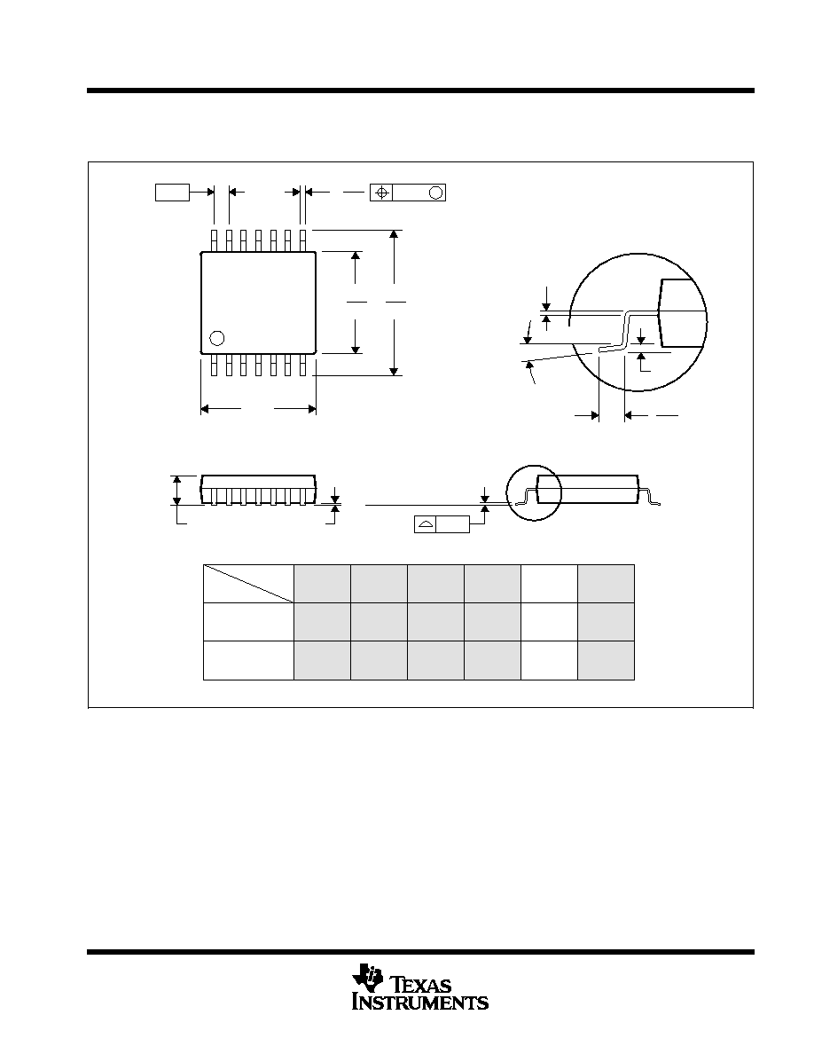
MECHANICAL DATA
PW (R-PDSO-G**)
PLASTIC SMALL-OUTLINE PACKAGE
4040064 / E 08/96
14 PIN SHOWN
Seating Plane
0,05 MIN
1,20 MAX
1
A
7
14
0,19
4,50
4,30
8
6,20
6,60
0,30
0,75
0,50
0,25
Gage Plane
0,15 NOM
0,65
M
0,10
0
°
8
°
0,10
PINS **
A MIN
A MAX
DIM
2,90
3,10
8
4,90
5,10
14
6,60
6,40
4,90
5,10
16
7,70
20
7,90
24
9,60
9,80
28
NOTES: A. All linear dimensions are in millimeters.
B. This drawing is subject to change without notice.
C. Body dimensions do not include mold flash or protrusion not to exceed 0,15.
D. Falls within JEDEC MO-153

IMPORTANT NOTICE
Texas Instruments (TI) reserves the right to make changes to its products or to discontinue any semiconductor
product or service without notice, and advises its customers to obtain the latest version of relevant information
to verify, before placing orders, that the information being relied on is current.
TI warrants performance of its semiconductor products and related software to the specifications applicable at
the time of sale in accordance with TI's standard warranty. Testing and other quality control techniques are
utilized to the extent TI deems necessary to support this warranty. Specific testing of all parameters of each
device is not necessarily performed, except those mandated by government requirements.
Certain applications using semiconductor products may involve potential risks of death, personal injury, or
severe property or environmental damage ("Critical Applications").
TI SEMICONDUCTOR PRODUCTS ARE NOT DESIGNED, INTENDED, AUTHORIZED, OR WARRANTED
TO BE SUITABLE FOR USE IN LIFE-SUPPORT APPLICATIONS, DEVICES OR SYSTEMS OR OTHER
CRITICAL APPLICATIONS.
Inclusion of TI products in such applications is understood to be fully at the risk of the customer. Use of TI
products in such applications requires the written approval of an appropriate TI officer. Questions concerning
potential risk applications should be directed to TI through a local SC sales office.
In order to minimize risks associated with the customer's applications, adequate design and operating
safeguards should be provided by the customer to minimize inherent or procedural hazards.
TI assumes no liability for applications assistance, customer product design, software performance, or
infringement of patents or services described herein. Nor does TI warrant or represent that any license, either
express or implied, is granted under any patent right, copyright, mask work right, or other intellectual property
right of TI covering or relating to any combination, machine, or process in which such semiconductor products
or services might be or are used.
Copyright
©
1998, Texas Instruments Incorporated