TRF1400
RF TELEMETRY RECEIVERS
VHF/UHF RZ ASK REMOTE CONTROL RECEIVER
SLWS014E JUNE 1996 REVISED APRIL 1998
1
POST OFFICE BOX 655303
·
DALLAS, TEXAS 75265
D
Wide VHF/UHF Frequency Range
200 MHz to 450 MHz for World-Wide
Remote Control Frequency Compatibility
D
High Receiver Sensitivity . . . 103 dBm at
315 MHz
D
Accepts Baseband Data Rates From 500 Hz
to 10 kHz
D
Manchester-Decoded and Raw Baseband
Outputs for Easy Interface to Serial Data
Decoders and Microcontrollers
D
TRF (Tuned Radio Frequency) Design
Eliminates Local Oscillator (No Emissions)
and Reduces Many Government Type
Approvals (Including FCC)
D
Adjustable Internal Sampling Clock Set By
External Components
D
Internal Amplifier and Comparator for
Amplification and Shaping of Low-Level
Input Signals With Average-Detecting
Autobias Adaptive Threshold Circuitry for
Improved Sensitivity
D
Minimum External Component Count and
Surface-Mount Packaging for Extremely
Small Circuit Footprint Typically Replaces
More Than 40 Components in an Equivalent
Discrete Solution
D
No Manual Alignment When Using SAW
Filters
D
Advanced Submicron BiCMOS Process
Technology for Minimum Power
Consumption
description
The TRF1400 VHF/UHF RZ ASK remote control
receiver is specifically designed for RZ ASK
(return-to-zero amplitude-shift keyed) commu-
nications systems operating in the 200-MHz to
450-MHz band. This device is targeted for use in
automotive and home security systems, garage
door openers, remote utility metering, and other
low-power remote control and telemetry systems.
A complete RZ ASK receiver solution on a chip,
the TRF1400 requires only a minimum of external
components for operation. This significantly
reduces the complexity and footprint of new
designs compared with current discrete receiver
designs. The TRF1400 requires no manual
alignment when using external SAW (surface
acoustic wave) filters. For a lower-cost solution,
the device is also compatible with external LC
components.
The TRF1400 also includes several on-chip features that normally require additional circuitry in a receiver
system design. These include two low-noise front-end amplifiers, an RF amplifier/comparator for detection and
shaping of input signals, and a demodulated RZ ASK baseband TTL-level output that readily interfaces to
self-synchronizing devices. Also included is on-chip Manchester decoding logic that provides a specially
formatted TTL data output, synchronized with a trigger output, for easy interface to any microcontroller using
Manchester-encoded data.
These devices have limited built-in ESD protection. The leads should be shorted together or the device placed in conductive foam
during storage or handling to prevent electrostatic damage to the MOS gates.
Please be aware that an important notice concerning availability, standard warranty, and use in critical applications of
Texas Instruments semiconductor products and disclaimers thereto appears at the end of this data sheet.
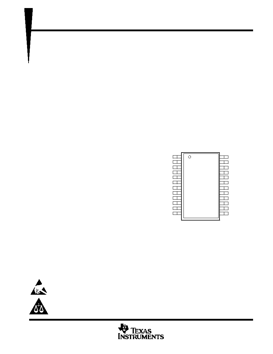
1
2
3
4
5
6
7
8
9
10
11
12
24
23
22
21
20
19
18
17
16
15
14
13
LPF
AGND
RFIN3
AVCC
AGND
AVCC
AGND
OFFSET
AGND
OSCR
OSCC
DVCC
RFOUT2
LNA2T
RFIN2
AGND
RFOUT1
LNA1T
RFIN1
AGND
DOUT
TRIG
BBOUT
DGND
DW PACKAGE
(TOP VIEW)
Copyright
©
1998, Texas Instruments Incorporated
PRODUCTION DATA information is current as of publication date.
Products conform to specifications per the terms of Texas Instruments
standard warranty. Production processing does not necessarily include
testing of all parameters.

TRF1400
RF TELEMETRY RECEIVERS
VHF/UHF RZ ASK REMOTE CONTROL RECEIVER
SLWS014E JUNE 1996 REVISED APRIL 1998
2
POST OFFICE BOX 655303
·
DALLAS, TEXAS 75265
description (continued)
The TRF1400 VHF/UHF RZ ASK remote control receiver is available in a 24-pin SOIC (DW) package, and is
characterized for operation over the temperature range of 40
°
C to 85
°
C. The DW package is available taped
and reeled; add R suffix to device type when ordering (e.g., TRF1400DWR).
functional block diagram
Summing
Amp
13
8
9
10
Manchester
Decoding
Logic
6
5
4
3
2
1
Clock
Comparator
+
11
12
14
15
16
17
18
19
20
21
22
23
24
LPF
AGND
RFIN3
AVCC
AGND
AVCC
AGND
7
OFFSET
AGND
OSCR
OSCC
DVCC
RFOUT2
LNA2T
RFIN2
AGND
RFOUT1
LNA1T
RFIN1
AGND
DOUT
TRIG
BBOUT
DGND
Six Log-Detecting
RF Amp Stages
Auto Level
SCLK
LNA2
LNA1

TRF1400
RF TELEMETRY RECEIVERS
VHF/UHF RZ ASK REMOTE CONTROL RECEIVER
SLWS014E JUNE 1996 REVISED APRIL 1998
3
POST OFFICE BOX 655303
·
DALLAS, TEXAS 75265
Terminal Functions
TERMINAL
I/O
DESCRIPTION
NAME
NO.
I/O
DESCRIPTION
AGND
2, 5,
7, 9,
17, 21
Analog ground for all internal analog circuits. AGND is not internally connected to digital ground (DGND). All
analog signals are referenced to AGND.
AVCC
4, 6
Positive power supply voltage for all analog circuits -- 4.5 V to 5.5 V
BBOUT
14
O
Baseband data output. BBOUT is the demodulated envelope of the recovered RF signal and is active with any
received ASK signal coding format.
DGND
13
Digital ground for all internal logic circuits. DGND is not internally connected to analog ground (AGND).
DOUT
16
O
Data output. Data appearing at DOUT is a binary, TTL representation of the baseband data, and is only meaningful
when Manchester-encoded ASK data is received. DOUT is active high and is internally pulled down.
DVCC
12
Positive power supply voltage for all digital circuits. DVCC is 4.5 V to 5.5 V. For best noise performance, DVCC
should connect to AVCC at the power supply, not at the TRF1400 device.
LNA1T
19
Low-noise amplifier (LNA) 1 ground termination. LNA1T should be connected to AGND through a parallel
resistor-capacitor bias network. If left unconnected, LNA1 is disabled.
LNA2T
23
Low-noise amplifier (LNA) 2 ground termination. LNA2T should be connected to AGND through a parallel
resistor-capacitor bias network. If left unconnected, LNA2 is disabled.
LPF
1
Connection for external low-pass capacitor used in the average-detecting adaptive threshold circuitry.
OFFSET
8
Connection for external offset resistor. A resistor (1 M
suggested) sets the internal threshold detector offset
voltage. Lowering the value of this resistor decreases device sensitivity.
OSCC
11
Internal oscillator frequency-setting capacitor. A capacitor, connected between OSCC and ground, in conjunction
with a resistor connected between OSCR and OSCC, determines the speed of the internal clock oscillator (SCLK).
The SCLK signal is used for processing the demodulated incoming data stream and controls the Manchester
decoding and timing recovery logic sections of the device. The internal oscillator must be set to 10 times the
received Manchester data rate for valid TRIG and DOUT, or to 5 times the received baseband data rate.
OSCR
10
Internal oscillator frequency-setting resistor. A resistor, connected between OSCR and OSCC, in conjunction with
a capacitor connected between OSCC and ground determines the speed of the internal oscillator (SCLK). The
SCLK signal is used for processing the demodulated incoming data stream and controls the Manchester decoding
and timing recovery logic sections of the device. The internal oscillator must be set to 10 times the received
Manchester data rate for valid TRIG and DOUT, or to 5 times the received baseband data rate.
RFIN1
18
I
RF input to first low-noise, high-gain amplifier stage
RFIN2
22
I
RF input to second low-noise, high-gain amplifier stage
RFIN3
3
I
RF input to the detecting RF amplifier stages. Filtered RF in the form of AM RZ ASK data at frequencies between
200 MHz and 450 MHz, at a baud rate between 500 Hz and 10 kHz can be applied to RFIN3 for detection and
decoding.
RFOUT1
20
O
RF output of the first low-noise, high-gain amplifier
RFOUT2
24
O
RF output of the second low-noise, high-gain amplifier. Typically, the input of an external SAW or LC filter is
connected to RFOUT2.
TRIG
15
O
Trigger output. TRIG pulses to indicate each new received data cell and is only meaningful when
Manchester-encoded ASK data is received. TRIG is active high and is internally pulled down.
TRF1400
RF TELEMETRY RECEIVERS
VHF/UHF RZ ASK REMOTE CONTROL RECEIVER
SLWS014E JUNE 1996 REVISED APRIL 1998
4
POST OFFICE BOX 655303
·
DALLAS, TEXAS 75265
absolute maximum ratings over operating free-air temperature range (unless otherwise noted)
Supply voltage range, AVCC, DVCC (see Note 1)
0.6 to 6 V
. . . . . . . . . . . . . . . . . . . . . . . . . . . . . . . . . . . . . . . .
Input voltage range, V
I
0.6 to 6 V
. . . . . . . . . . . . . . . . . . . . . . . . . . . . . . . . . . . . . . . . . . . . . . . . . . . . . . . . . . . . . . .
Continuous total power dissipation
180 mW
. . . . . . . . . . . . . . . . . . . . . . . . . . . . . . . . . . . . . . . . . . . . . . . . . . . . . . . .
Operating free-air temperature range, T
A
55
°
C to 85
°
C
. . . . . . . . . . . . . . . . . . . . . . . . . . . . . . . . . . . . . . . . . . . .
Storage temperature range, T
stg
65
°
C to 150
°
C
. . . . . . . . . . . . . . . . . . . . . . . . . . . . . . . . . . . . . . . . . . . . . . . . . . .
ESD protection, all terminals: human body model
2 kV
. . . . . . . . . . . . . . . . . . . . . . . . . . . . . . . . . . . . . . . . . . . . .
machine model
200 V
. . . . . . . . . . . . . . . . . . . . . . . . . . . . . . . . . . . . . . . . . . . . . . .
JEDEC latchup
150 mA or 11 V
. . . . . . . . . . . . . . . . . . . . . . . . . . . . . . . . . . . . . . . . . . . . . . . . . . . . . . . . . . . . . . . . . .
Stresses beyond those listed under "absolute maximum ratings" may cause permanent damage to the device. These are stress ratings only, and
functional operation of the device at these or any other conditions beyond those indicated under "recommended operating conditions" is not
implied. Exposure to absolute-maximum-rated conditions for extended periods may affect device reliability.
NOTE 1: Voltage values are with respect to GND.
recommended operating conditions
MIN
NOM
MAX
UNIT
Supply voltage, VCC
4.5
5.5
V
Input frequency, fin
200
450
MHz
Operating free-air temperature, TA
40
85
°
C
Minimum permissible AM modulation of RF envelope applied to RF Input, measured at 101 dBm
25%
electrical characteristics as measured in the test circuit detailed in Figures 1 through 6 with
f
in
= 315 MHz over recommended ranges of supply voltage and operating free-air temperature,
typical values are at V
CC
= 5 V and T
A
= 25
°
C (unless otherwise noted)
current consumption
PARAMETER
TEST CONDITIONS
MIN
TYP
MAX
UNIT
I/O pins terminated with typical loads,
Signal applied with a 5-kHz baseband data rate
2.7
3.5
ICC
Average supply current from VCC
I/O pins terminated with typical loads,
Signal applied with a 2.5-kHz Manchester data rate
2.7
3.5
mA
I/O pins terminated with typical loads, no data input
2.5
digital interface
PARAMETER
TEST CONDITIONS
MIN
MAX
UNIT
VOH
High-level output voltage
DOUT TRIG BBOUT
IOH = 3.2 mA
VCC 0.5
V
VOL
Low-level output voltage
DOUT, TRIG, BBOUT
IOL = 3.2 mA
0.5
V
VSWR (voltage standing-wave ratio), ripple rejection
PARAMETER
TEST CONDITIONS
MIN
TYP
MAX
UNIT
VSWR into 50
at RFIN1, RFOUT1, RFIN2, RFOUT2,
RFIN3
With external LC matching network
2:1
V/V
Ripple rejection at BBOUT while maintaining
BER = 1/100 (see Note 2)
1 MHz injected at AVCC and DVCC,
Carrier level = 50 dBm
6% VCC
NOTE 2: BER (bit error rate = errors/number of bits) is qualified by integration of logic-level pulses (> 50% high = 1, < 50% low = 0). (See the
System Design Considerations Using the TRF1400 RF Telemetry Receivers Application Report, TI literature number SLWA005, for
more BER information.)

TRF1400
RF TELEMETRY RECEIVERS
VHF/UHF RZ ASK REMOTE CONTROL RECEIVER
SLWS014E JUNE 1996 REVISED APRIL 1998
5
POST OFFICE BOX 655303
·
DALLAS, TEXAS 75265
RF sensitivity/overload
PARAMETER
TEST CONDITIONS
MIN
TYP
MAX
UNIT
RF input level (average) at test board RF input required for BER
1/100 at 5 kHz baseband data rate
VCC = 5 V,
TA = 25
°
C,
fin = 315 MHz,
103
101
dBm
1/100 at 5 kHz baseband data rate,
2.5 kHz Manchester data rate (see Note 2)
in
,
external SAW preselector bandpass
filter (see Note 3)
103
101
dBm
Overload signal level at fc with BER 1/100 at 5 kHz baseband
data rate, 2.5 kHz Manchester data rate (see Note 2)
VCC = 5 V,
fin = 315 MHz
TA = 25
°
C,
20
dBm
NOTES:
2. BER (bit error rate = errors/number of bits) is qualified by integration of logic-level pulses (> 50% high = 1, < 50% low = 0).
3. The SAW bandpass filter must have a rejection level greater than or equal to 50 dB at
±
0.5 fc, an insertion loss of less than or equal
to 3 dB, and a 3 dB passband width of 0.2% fc, where fc is the passband center frequency of the SAW filter.
oscillator (internal clock)
PARAMETER
MIN
MAX
UNIT
Sample clock frequency, SCLK (5
×
baseband data rate, 10
×
Manchester data rate)
2.5
50
kHz
Frequency spread (process variation, temperature, VCC), not including external component tolerance
±
5%
timing requirements over recommended ranges of supply voltage and operating free-air
temperature
RF input data (see Figure 7)
MIN
MAX
UNIT
tr
Rise time at RFIN1
0.1 tw3
µ
s
tf
Fall time at RFIN1
0.1 tw3
µ
s
received data
MIN
MAX
UNIT
Baseband data frequency, AM RZ ASK
0.5
10
kHz
Manchester data frequency, AM RZ ASK
0.25
5
kHz
Pulse period tolerance for synchronization, valid TRIG and DOUT data
±
8%
Pulse duty cycle for synchronization, valid TRIG and DOUT data
49%
51%
tx
Dead time between wakeup time and frame start time (for synchronization valid, TRIG and
DOUT data) (see Figure 8)
38
÷
SCLK
317
÷
SCLK
ms
tw3
Duration, modulated RF carrier (see Figure 9)
100
2000
µ
s
switching characteristics over recommended ranges of supply voltage and operating free-air
temperature
device latency for BBOUT, TRIG, DOUT (see Figure 9)
PARAMETER
MIN
TYP
MAX
UNIT
Delay time between power applied and output signal at BBOUT
10
ms
Demodulation delay time across device (RF Input to BBOUT)
10
µ
s
td1
Delay time between BBOUT
and TRIG
2.5
÷
SCLK
µ
s
td2
Delay time between DOUT
and TRIG
0.5
÷
SCLK
µ
s
RF carrier (see Figure 9)
PARAMETER
MIN
TYP
MAX
UNIT
tw0
Duration, logic 0 data cell
2 tw3
µ
s
tw1
Duration, logic 1 data cell
2 tw3
µ
s
tw2
Duration, trigger pulse
0.5
÷
SCLK
µ
s