Actual Size
(2,15 mm x 2,3 mm)
www.ti.com
FEATURES
APPLICATIONS
DESCRIPTION
3
2
4
5
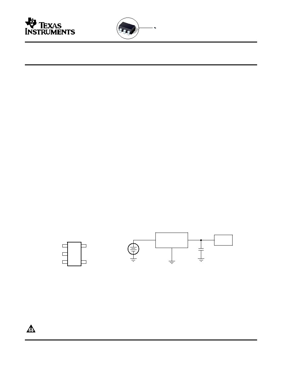
DCK PACKAGE
(TOP VIEW)
1
FB/NC
GND
NC
OUT
IN
GND
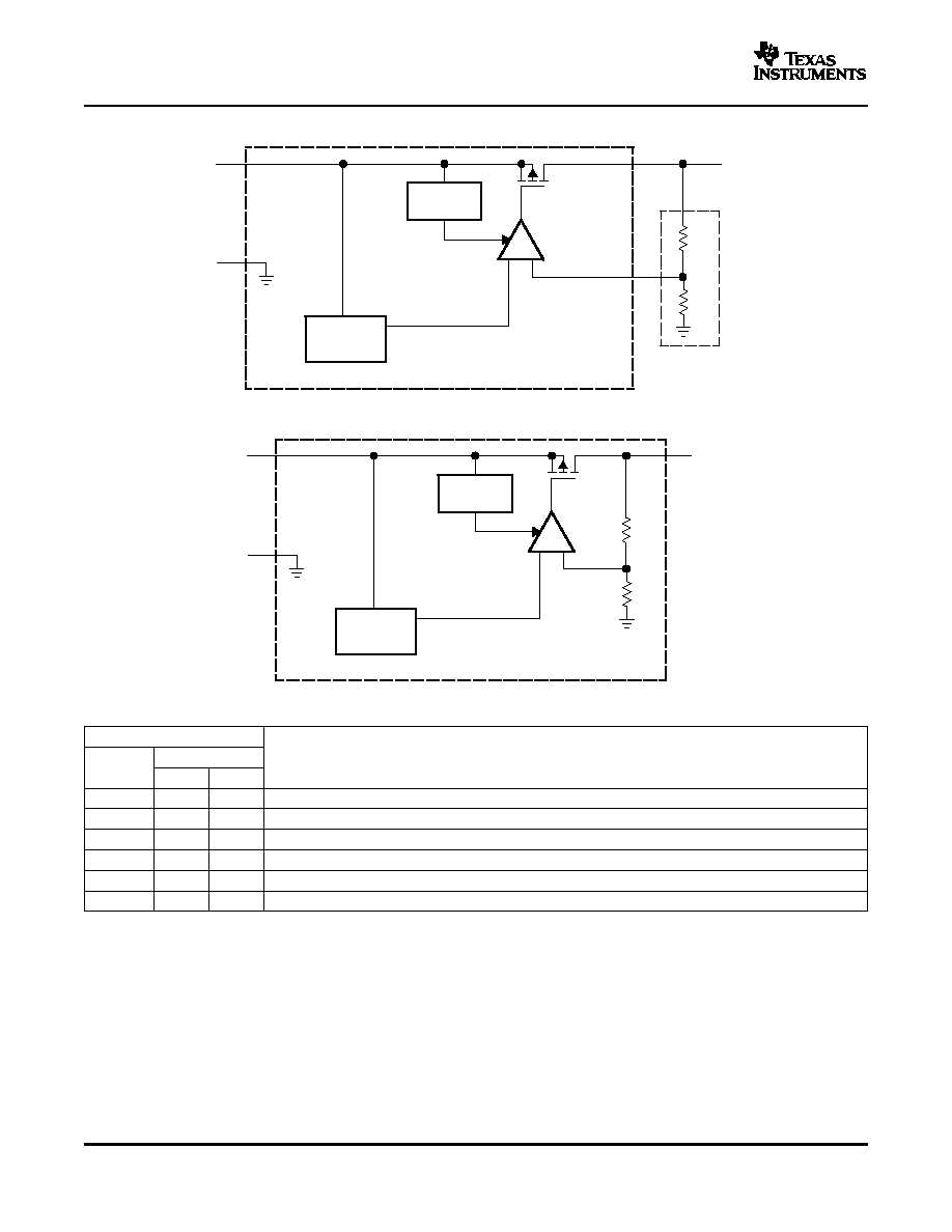
TPS715xx
OUT
IN
MSP430
Solar
Cell
TPS715xx
SLVS338L MAY 2001 REVISED SEPTEMBER 2005
50 mA, 24 V, 3.2 µA Supply Current
Low-Dropout Linear Regulator in SC70 Package
·
Ultra Low Power Microcontrollers
·
24-V Maximum Input Voltage
·
Cellular/Cordless Handsets
·
Low 3.2-µA Quiescent Current at 50 mA
·
Portable/Battery-Powered Equipment
·
Stable With Any Capacitor (
0.47 µF)
·
50-mA Low-Dropout Regulator
·
Available in 1.8 V, 1.9 V, 2.3 V, 2.5 V, 3.0 V, 3.3
The TPS715xx low-dropout (LDO) voltage regulators
V, 3.45 V, 5.0 V, and Adjustable (1.2 V to 15 V)
offer the benefits of high input voltage, low-dropout
·
Designed to Support MSP430 Families:
voltage,
low-power
operation,
and
miniaturized
1.9 V version ensured to be higher than
packaging. The devices, which operate over an input
minimum V
IN
of 1.8 V
range of 2.5 V to 24 V, are stable with any capacitor
(
0.47 µF). The low dropout voltage and low
2.3 V version ensured to meet 2.2 V
quiescent current allow operations at extremely low
minimum V
IN
for FLASH on MSP430F2xx
power levels. Therefore, the devices are ideal for
3.45 V version ensured to be lower than
powering battery management ICs. Specifically, since
maximum V
IN
of 3.6 V
the devices are enabled as soon as the applied
voltage reaches the minimum input voltage, the
Wide variety of fixed output voltage options
output is quickly available to power continuously
to match V
IN
to the minimum required for
operating battery charging ICs.
desired MSP430 speed
The usual PNP pass transistor has been replaced by
·
Minimum/Maximum Specified Current Limit
a PMOS pass element. Because the PMOS pass
·
5-Pin SC70/SOT-323 (DCK) Package
element behaves as a low-value resistor, the low
·
-40°C to +125°C Specified Junction
dropout voltage, typically 415 mV at 50 mA of load
Temperature Range
current, is directly proportional to the load current.
The low quiescent current (3.2 µA typically) is stable
·
For 80mA Rated Current and Higher Power
over the entire range of output load current (0 mA to
Package, see
TPS715Axx
50 mA).
Please be aware that an important notice concerning availability, standard warranty, and use in critical applications of Texas
Instruments semiconductor products and disclaimers thereto appears at the end of this data sheet.
All trademarks are the property of their respective owners.
PRODUCTION DATA information is current as of publication date.
Copyright © 20012005, Texas Instruments Incorporated
Products conform to specifications per the terms of the Texas
Instruments standard warranty. Production processing does not
necessarily include testing of all parameters.
www.ti.com
ABSOLUTE MAXIMUM RATINGS
DISSIPATION RATING TABLE
TPS715xx
SLVS338L MAY 2001 REVISED SEPTEMBER 2005
This integrated circuit can be damaged by ESD. Texas Instruments recommends that all integrated
circuits be handled with appropriate precautions. Failure to observe proper handling and installation
procedures can cause damage.
ESD damage can range from subtle performance degradation to complete device failure. Precision
integrated circuits may be more susceptible to damage because very small parametric changes could
cause the device not to meet its published specifications.
ORDERING INFORMATION
(1)
PRODUCT
V
OUT
(2)
TPS715xxyyyz
XX is nominal output voltage (for example, 28 = 2.8V, 285 = 2.85V, 01 = Adjustable).
YYY is package designator.
Z is package quantity.
(1)
For the most current package and ordering information, see the Package Option Addendum at the end of this document, or see the TI
website at
www.ti.com
.
(2)
Output voltages from 1.25V to 5.4V in 50mV increments are available through the use of innovative factory EEPROM programming;
minimum order quantities may apply. Contact factory for details and availability.
over operating temperature range (unless otherwise noted)
(1) (2)
UNIT
V
IN
range
-0.3 V to 24 V
Peak output current
Internally limited
ESD rating, HBM
2 kV
ESD rating, CDM
500 V
Continuous total power dissipation
See Dissipation Rating Table
Junction temperature range, T
J
-40°C to +150°C
Storage temperature range, T
stg
-65°C to +150°C
(1)
Stresses beyond those listed under absolute maximum ratings may cause permanent damage to the device. These are stress ratings
only, and functional operation of the device at these or any other conditions beyond those indicated under recommended operating
conditions is not implied. Exposure to absolute-maximum-rated conditions for extended periods may affect device reliability.
(2)
All voltage values are with respect to network ground terminal.
DERATING FACTOR
T
A
25°C
T
A
= 70°C
T
A
= 85°C
BOARD
PACKAGE
R
JC
°C/W
R
JA
°C/W
ABOVE T
A
= 25°C
POWER RATING
POWER RATING
POWER RATING
Low-K
(1)
DCK
165
395
2.52 mW/°C
250 mW
140 mW
100 mW
High-K
(2)
DCK
165
315
3.18 mW/°C
320 mW
175 mW
130 mW
(1)
The JEDEC Low-K (1s) board design used to derive this data was a 3 inch x 3 inch, two-layer board with 2 ounce copper traces on top
of the board.
(2)
The JEDEC High-K (2s2p) board design used to derive this data was a 3 inch x 3 inch, multilayer board with 1 ounce internal power and
ground planes and 2 ounce copper traces on top and bottom of the board.
2