
(6,6 mm x 6,4 mm)
(4,15 mm x 4,15 mm)
www.ti.com
FEATURES
APPLICATIONS
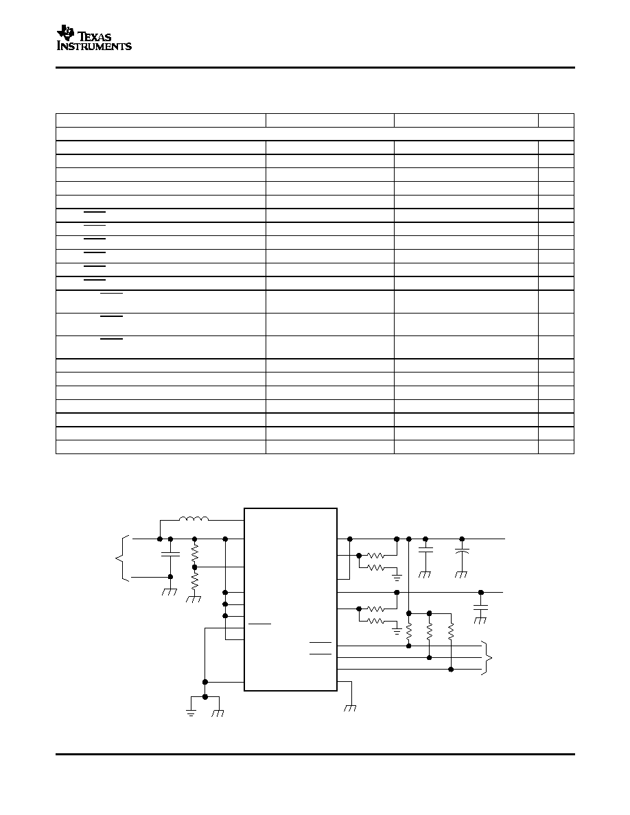
TYPICAL APPLICATION
OFF
ON
OFF
ON
OFF
ON
OFF
ON
OFF
ON
VBAT
LBI
SKIPEN
ADEN
EN
ENPB
LDOEN
SWN
VOUT
FB
PGOOD
LBO1
LBO2
LDOIN
LDOOUT
LDOSENSE
GND
PGND
Control
Inputs
Control
Outputs
V
CC1
V
CC2
TPS61100
Battery
TPS61100, TPS61103
TPS61106, TPS61107
SLVS411B JUNE 2002 REVISED APRIL 2004
DUAL-OUTPUT, SINGLE-CELL BOOST CONVERTER
·
Low EMI-Converter (Integrated Antiringing
Switch)
·
Synchronous 95% Efficient Boost Converter
·
Load Disconnect During Shutdown
·
Integrated 120 mA LDO for Second Output
·
Auto Discharge Allows the Device to
Voltage
Discharge Output Capacitor During Shutdown
·
TSSOP-20 and QFN-24 Package
·
Overtemperature Protection
·
65 µA (Typ) Total Device Quiescent Current
·
EVM Available (TPS6110XEVM-216)
·
0.8 V to 3.3 V Input Voltage Range
·
Adjustable Output Voltage up to 5.5 V and
Fixed Output Voltage Options
·
All Single or Dual Cell Battery Operated
Products Which Use Two System Voltages
·
Power-Save Mode for Improved Efficiency at
Like DSP C5X Applications
Low Output Power
·
Internet Audio Player, PDAs, Digital Still
·
Battery Supervision
Cameras and Other Portable Equipment
·
Power Good Output
·
Pushbutton Function for Start-Up
Please be aware that an important notice concerning availability, standard warranty, and use in critical applications of Texas
Instruments semiconductor products and disclaimers thereto appears at the end of this data sheet.
PRODUCTION DATA information is current as of publication date.
Copyright © 20022004, Texas Instruments Incorporated
Products conform to specifications per the terms of the Texas
Instruments standard warranty. Production processing does not
necessarily include testing of all parameters.

www.ti.com
DESCRIPTION
TPS61100, TPS61103
TPS61106, TPS61107
SLVS411B JUNE 2002 REVISED APRIL 2004
These devices have limited built-in ESD protection. The leads should be shorted together or the device
placed in conductive foam during storage or handling to prevent electrostatic damage to the MOS gates.
The TPS6110x devices provide a complete power supply solution for products powered by either one or two
Alkaline, NiCd, or NiMH battery cells. The converter generates two stable output voltages that are either adjusted
by an external resistor divider or fixed internally on the chip. It stays in operation with supply voltages down to
0.8 V. The implemented boost converter is based on a fixed frequency, pulse-width-modulation (PWM) controller
using a synchronous rectifier to obtain maximum efficiency.
The maximum peak current in the boost switch is limited to a value of 1800 mA.
The converter can be disabled to minimize battery drain. During shutdown, the load is completely disconnected
from the battery. An auto discharge function allows discharging the output capacitors during shutdown mode.
This is especially useful in microcontroller applications where the microcontroller or microprocessor should not
remain active due to the stored voltage on the output capacitors. Programming the ADEN-pin disables this
feature. A low-EMI mode is implemented to reduce ringing and in effect lower radiated electromagnetic energy
when the converter enters the discontinuous conduction mode. A power good output at the boost stage provides
additional control of cascaded power supply components.
The built-in LDO can be used for a second output voltage derived either from the boost output or directly from
the battery. The output voltage of this LDO can be programmed by an external resistor divider or is fixed
internally on the chip. The LDO can be enabled separately i.e., using the power good of the boost stage.
The device is packaged in a 20-pin TSSOP (20 PW) package or in a 24-pin QFN (24 RGE) package.
AVAILABLE PACKAGE OPTIONS
PACKAGE
CODE
20-Pin TSSOP
PW
24-Pin QFN
RGE
AVAILABLE OUTPUT VOLTAGE OPTIONS
OUTPUT
OUTPUT
T
A
VOLTAGE
VOLTAGE
PART NUMBER
(1)
PART NUMBER
(1)
DC/DC
LDO
Adjustable
Adjustable
TPS61100PW
TPS61100RGE
3.3 V
Adjustable
TPS61103PW
TPS61103RGE
40
°
C to 85
°
C
3.3 V
1.5 V
TPS61106PW
TPS61106RGE
3.3 V
1.8 V
TPS61107PW
TPS61107RGE
(1)
The PW package is available taped and reeled. Add R suffix to device type (e.g., TPS61100PWR) to
order quantities of 2000 devices per reel. The RGE package is only available in reels. Add R suffix to
device type (e.g. TPS61100RGER) to order quantities of 3000 devices per reel.
2

www.ti.com
Anti-
Ringing
Gate
CONTROL
PGND
Regulator
Error
Amplifier
Auto
Discharge
PGND
Control Logic
V
ref
Oscillator
Temperature
Control
Low Dropout
Regulator
Auto
Discharge
GND
Low Battery
Comparator
VOUT
PGND
FB
LDOIN
LDOOUT
LDOSENSE
SWN
VBAT
EN
ENPB
PGOOD
LDOEN
SKIPEN
ADEN
GND
LBI
LBO1
LBO2
TPS61100, TPS61103
TPS61106, TPS61107
SLVS411B JUNE 2002 REVISED APRIL 2004
FUNCTIONAL BLOCK DIAGRAM
3

www.ti.com
1
2
3
4
5
6
7
8
9
10
20
19
18
17
16
15
14
13
12
11
VBAT
LBI
ENPB
EN
ADEN
LDOSENSE
LDOEN
LDOIN
LDOOUT
GND
FB
VOUT
SKIPEN
NC
SWN
PGOOD
SWN
LBO2
LBO1
PGND
PW PACKAGE
(TOP VIEW)
VBA
T
LBI
ENPB
EN
ADEN
LDOIN
LDOEN
LDOSENSE
LBO2
SWN
PGOOD
SWN
SKIPEN
VOUT
FB
TPS6110X
LDOOUT
GND
LBO1
PGND
NC
PGND
SWN
SWN
VOUT
RGE PACKAGE
(TOP VIEW)
NC No internal connection
TPS61100, TPS61103
TPS61106, TPS61107
SLVS411B JUNE 2002 REVISED APRIL 2004
Terminal Functions
TERMINAL
NO.
I/O
DESCRIPTION
NAME
PW
RGE
ADEN
5
3
I
Auto discharge enable (1/VBAT enabled, 0/GND disabled)
EN
4
2
I
Boost-enable input. (1/VBAT enabled, 0/GND disabled)
ENPB
3
24
I
Boost-enable input (pushbutton). (0/GND enabled. 1/VBAT disabled)
FB
20
21
I
Boost-voltage feedback of adjustable versions
GND
10
8
I/O
Control/logic ground
LBI
2
23
I
Low battery comparator input (comparator enabled with EN)
LBO1
12
11
O
Low battery comparator output 1 (open drain)
LBO2
13
12
O
Low battery comparator output 2 (open drain)
LDOEN
7
5
I
LDO-enable input (1/VBAT enabled, 0/GND disabled)
LDOOUT
9
7
O
LDO output
LDOIN
8
6
I
LDO input
LDOSENSE
6
4
I
LDO feedback for voltage adjustment, must be connected to LDOOUT at fixed output voltage
versions
NC
17
1
No connection
PGND
11
9, 10
I/O
Power ground
PGOOD
15
15
O
Boost output power good (1 : good, 0 : failure) (open drain)
SKIPEN
18
18
I
Enable/disable Power save mode (1: VBAT enabled, 0: GND disabled)
SWN
14, 16
13, 14,
I
Boost switch input
16, 17
VBAT
1
22
I
Supply pin
VOUT
19
19, 20
O
Boost output
4

www.ti.com
DETAILED DESCRIPTION
SYNCHRONOUS RECTIFIER
CONTROLLER CIRCUIT
DEVICE ENABLE
LDO ENABLE
POWER GOOD
TPS61100, TPS61103
TPS61106, TPS61107
SLVS411B JUNE 2002 REVISED APRIL 2004
The device integrates an N-channel and a P-channel MOSFET transistor to realize a synchronous rectifier.
Because the commonly used discrete Schottky rectifier is replaced with a low RDS(ON) PMOS switch, the power
conversion efficiency reaches 95%. To avoid ground shift due to the high currents in the NMOS switch, two
separate ground pins are used. The reference for all control functions is the GND pin. The source of the NMOS
switch is connected to PGND. Both grounds must be connected on the PCB at only one point close to the GND
pin. A special circuit is applied to disconnect the load from the input during shutdown of the converter. In
conventional synchronous rectifier circuits, the backgate diode of the high-side PMOS is forward biased in
shutdown and allows current flowing from the battery to the output. This device however uses a special circuit
which takes the cathode of the backgate diode of the high-side PMOS and disconnects it from the source when
the regulator is not enabled (EN = low).
The benefit of this feature for the system design engineer is that the battery is not depleted during shutdown of
the converter. No additional components have to be added to the design to make sure that the battery is
disconnected from the output of the converter.
The controller circuit of the device is based on a fixed frequency multiple feedforward controller topology. Input
voltage, output voltage, and voltage drop on the NMOS switch are monitored and forwarded to the regulator. So
changes in the operating conditions of the converter directly affect the duty cycle and must not take the indirect
and slow way through the control loop and the error amplifier. The control loop, determined by the error amplifier,
only has to handle small signal errors. The input for it is the feedback voltage on the FB pin or, at fixed output
voltage versions, the voltage on the internal resistor divider. It is compared with the internal reference voltage to
generate an accurate and stable output voltage.
The peak current of the NMOS switch is also sensed to limit the maximum current flowing through the switch and
the inductor. The nominal peak current limit is set to 1500 mA.
An internal temperature sensor prevents the device from getting overheated in case of excessive power
dissipation.
The device is put into operation when EN is set high. It is put into a shutdown mode when EN is set to GND. It
also can be enabled with a low signal on ENPB. This forces the converter to start up as long as the low signal is
applied. During this time EN must be set high to prevent the converter from going down into shutdown mode
again. If EN is high, a negative signal on ENPB is ignored.
In shutdown mode, the regulator stops switching, all internal control circuitry including the low-battery comparator
is switched off, and the load is isolated from the input (as described in the synchronous rectifier section). This
also means that the output voltage can drop below the input voltage during shutdown. During start-up of the
converter, the duty cycle and the peak current are limited in order to avoid high peak currents drawn from the
battery.
An undervoltage lockout function prevents device start-up if the supply voltage on VBAT is lower than
approximately 0.7 V. When in operation and the battery is being discharged, the device automatically enters the
shutdown mode if the voltage on VBAT drops below approximately 0.7 V. This undervoltage lockout function is
implemented in order to prevent the malfunctioning of the converter.
When the voltage is applied at VBAT, the LDO can be separately enabled and disabled by using the LDOEN pin
in the same way as the EN pin at the dc/dc converter stage described above.
The PGOOD pin stays high impedance when the dc/dc converter delivers an output voltage within a defined
voltage window. So it can be used to enable the converter after pushbutton start-up, or to enable any connected
circuitry such as cascaded converters (LDO) or processor circuits.
5

www.ti.com
POWER SAVE MODE
AUTO DISCHARGE
LOW BATTERY DETECTOR CIRCUIT--LBI/LBO
LOW-EMI SWITCH
LDO
TPS61100, TPS61103
TPS61106, TPS61107
SLVS411B JUNE 2002 REVISED APRIL 2004
DETAILED DESCRIPTION (continued)
The SKIPEN pin can be used to select different operation modes. To enable power save, SKIPEN must be set
high. Power save mode is used to improve efficiency at light load. In power save mode the converter only
operates when the output voltage trips below a set threshold voltage. It ramps up the output voltage with one or
several pulses and goes again into power save mode once the output voltage exceeds the set threshold voltage.
This power save mode can be disabled by setting the SKIPEN to GND.
The auto discharge function is needed in applications where the supply voltage of a microcontroller,
microprocessor or memory has to be removed during shutdown in order to make sure that the system quickly
goes in a defined state. The auto discharge function is enabled when the ADEN is set high. It is disabled when
the ADEN is set to GND. When the auto discharge function is enabled, the output capacitor is discharged after
the device is programmed in the shutdown mode. The output capacitor is discharged by an integrated switch of
400
, hence the discharge time depends on the size of the output capacitor.
The low-battery detector circuit is typically used to supervise the battery voltage and to generate an error flag
when the battery voltage drops below a user-set threshold voltage. The function is active only when the device is
enabled. When the device is disabled, both LBO-pin are high-impedance. There are three programmed
thresholds, 400 mV, 450 mV, and 500 mV. The outputs on LBO1 and LBO2 are shown as follows:
LBI INPUT
LBO1
LBO2
(mV)
0-400
0
0
400-450
1
0
450-500
0
1
500-VBAT
1
1
1 means that the output stays at high-impedance and 0 means that the output goes active low. If there is only
one LBO output needed, both outputs can be tied together. Then the switching threshold is at 500 mV at LBI.
The battery voltage, at which the detection circuit switches, can be programmed with a resistive divider
connected to the LBI-pin. The resistive divider scales down the battery voltage to a voltage level of 400 mV
(450 mV, 500 mV), which is then compared to the LBI threshold voltage. The LBI-pin has a built-in hysteresis of
10 mV. See the application section for more details about the programming of the LBI-threshold. If the
low-battery detection circuit is not used, the LBI-pin should be connected to GND (or to VBAT) and the LBO-pin
can be left unconnected. Do not let the LBI-pin float.
The device integrates a circuit that removes the ringing that typically appears on the SW-node when the
converter enters discontinuous current mode. In this case, the current through the inductor ramps to zero and the
rectifying PMOS switch is turned off to prevent a reverse current flowing from the output capacitors back to the
battery. Due to the remaining energy that is stored in parasitic components of the semiconductor and the
inductor, a ringing on the SW-pin is induced. The integrated antiringing switch clamps this voltage to VBAT and
therefore dampens ringing.
The built-in LDO can be used to generate a second output voltage derived from the dc/dc converter output, from
the battery, or from another power source like an ac adapter or a USB power rail. The LDOSENSE input must be
connected to LDOOUT at fixed output voltage versions.
6

www.ti.com
ABSOLUTE MAXIMUM RATINGS
(1)
RECOMMENDED OPERATING CONDITIONS
TPS61100, TPS61103
TPS61106, TPS61107
SLVS411B JUNE 2002 REVISED APRIL 2004
over operating free-air temperature range (unless otherwise noted)
UNIT
Input voltage range on VBAT, LBI, SKIPEN, EN, ENPB, ADEN, FB, LDOEN
-0.3 V to 3.6 V
Input voltage range on SWN, VOUT, LDOIN, LDOOUT, LDOSENSE, PGOOD, LBO1, LBO2
-0.3 V to 7 V
Operating free air temperature range, T
A
-40
°
C to 85
°
C
Maximum junction temperature, T
J
150
°
C
Storage temperature range, T
stg
-65
°
C to 150
°
C
Lead temperature 1,6 mm (1/16 inch) from case for 10s
260
°
C
(1)
Stresses beyond those listed under,, absolute maximum ratings" may cause permanent damage to the device. These are stress ratings
only, and functional operation of the device at these or any other conditions beyond those indicated under,, recommended operating
conditions" is not implied. Exposure to absolute-maximum-rated conditions for extended periods may affect device reliability.
MIN NOM
MAX
UNIT
V
I
Supply voltage at VBAT
0.8
3.3
V
L
Boost--inductor
4.7
10
µH
C
i
Boost--input capacitor
10
µF
C
o
Boost--output capacitor
22
100
µF
C
i
LDO--input capacitor
1
µF
C
o
LDO--output capacitor
1
2.2
µF
T
J
Operating virtual junction temperature
-40
125
°
C
7

www.ti.com
ELECTRICAL CHARACTERISTICS
TPS61100, TPS61103
TPS61106, TPS61107
SLVS411B JUNE 2002 REVISED APRIL 2004
over recommended free-air temperature range and over recommended input voltage range (typical at an ambient temperature
range of 25
°
C) (unless otherwise noted)
PARAMETER
TEST CONDITIONS
MIN
TYP
MAX
UNIT
BOOST STAGE
Input voltage for start-up
R
L
> = 66
at V
o
= 3.3 V
0.85
1.1
V
V
I(b)
Input voltage once started
0.8
3.3
V
V
o(b)
Output voltage
1.5
5.5
V
Minimum possible output power
PW package, VBAT
1.5 V
600
mW
V
ref
Reference voltage
485
500
515
mV
f
Oscillator frequency
320
500
800
kHz
Switch current limit
V
o
= 3.3 V
1200
1500
1800
mA
Startup current limit
610
mA
Boost switch on resistance
V
o
= 3.3 V
180
300
m
Sync switch on resistance
V
o
= 3.3 V
180
300
m
Total accuracy
-3%
3%
Auto discharge switch resistance
400
VBAT
I
O
= 0 mA, V
EN
= VBAT = 3.3 V, V
o
= 3.3 V, ENLDO = 0
25
40
µA
Boost quiescent current
VOUT
I
O
= 0 mA, V
EN
= VBAT = 3.3 V, V
o
= 3.3 V, ENLDO = 0
12
20
µA
Boost shutdown current
V
EN
= 0 V
0.5
5
µA
LDO STAGE
V
I(LDO)
Input voltage range
1.5
7
V
V
o(LDO)
Output voltage
0.9
3.6
V
V
I
1.8 V
120
270
I
o(LDO)
Output current
mA
V
I
< 1.8 V
80
LDO short circuit current limit
500
mA
Minimum voltage drop
V
I
1.8 V, I
o(LDO)
= 120 mA
300
mV
Total accuracy
I
o
1 mA
±
3%
Line regulation
LDOIN change form 1.8 V to 2.6 V at 100 mA
0.6%
Load regulation
Load change from 10% to 90%
0.6%
Auto discharge switch resistance
400
LDOIN
27
40
LDO quiescent current
LDOIN = 7 V, VBAT = 1.2 V, EN = 0
µA
VBAT
27
40
LDO shutdown current
0.01
1
µA
8
www.ti.com
ELECTRICAL CHARACTERISTICS (CONTINUED)
PARAMETER MEASUREMENT INFORMATION
SWN
C3
10
µ
F
Power
Supply
L1
10
µ
H
R1
R2
VBAT
VOUT
FB
R3
R6
LDOIN
R5
R4
LDOSENSE
LDOOUT
R7
R8
R9
C6
2.2
µ
F
C4
100
µ
F
U1
LBO1
LBO2
PGOOD
PGND
LBI
SKIPEN
ADEN
EN
ENPB
LDOEN
GND
TPS6110x
List of Components:
U1 = TPS6110x
L1 = SUMIDA CDRH74100
C3, C5, C6 = X7R/X5R Ceramic
C4 = Low ESR Tantalum
V
CC1
Boost Output
V
CC2
LDO Output
Control
Outputs
C5
TPS61100, TPS61103
TPS61106, TPS61107
SLVS411B JUNE 2002 REVISED APRIL 2004
over recommended free-air temperature range and over recommended input voltage range (typical at an ambient temperature
range of 25
°
C) (unless otherwise noted)
PARAMETER
TEST CONDITIONS
MIN
TYP
MAX
UNIT
CONTROL STAGE
V
IL
LBI1 voltage threshold
V
LBI
voltage decreasing
390
400
410
mV
LBI2 voltage threshold
V
LBI
voltage decreasing
440
450
460
mV
LBI3 voltage threshold
V
LBI
voltage decreasing
490
500
510
mV
LBI input hysteresis
10
mV
LBI input current
EN = Vbat or GND
0.01
0.1
µA
LBO1 output low voltage
V
o
= 3.3 V, I
OL
= 10 µA
0.04
0.4
V
LBO1 output low current
10
µA
LBO1 output leakage current
V
LBO
= 3.3 V
0.01
0.1
µA
LBO2 output low voltage
V
o
= 3.3 V, I
OL
= 10 µA
0.04
0.4
V
LBO2 output low current
10
µA
LBO2 output leakage current
V
LBO
= 3.3 V
0.01
0.1
µA
EN, ENPB, LDOEN, SKIPEN and ADEN input
V
IL
0.2
×
VBAT
low voltage
EN, ENPB, LDOEN, SKIPEN and ADEN input
V
IH
0.8
×
VBAT
high voltage
EN, ENPB, LDOEN, SKIPEN and ADEN input
Clamped on GND or VBAT
0.01
0.1
µA
current
Powergood threshold
V
o
= 3.3 V
0.9xV
o
0.92xV
o
0.95xV
o
Powergood delay
30
µs
Powergood output low voltage
V
o
= 3.3 V, I
OL
= 10 µA
0.04
0.4
V
Powergood output low current
10
µA
Powergood output leakage current
0.01
0.1
µA
Overtemperature protection
140
°
C
Overtemperature hysteresis
20
°
C
9

www.ti.com
TYPICAL CHARACTERISTICS
TPS61100, TPS61103
TPS61106, TPS61107
SLVS411B JUNE 2002 REVISED APRIL 2004
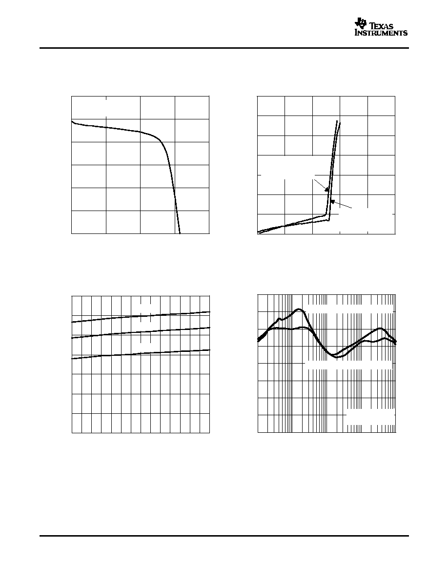
Table of Graphs
BOOST CONVERTER
Figure
vs Input voltage for VOUT = 3.3 V, 5.0 V
1
Maximum output current
vs Input voltage for VOUT = 1.8 V, 2.5 V
2
vs Output current for VIN = 1.2 V, VOUT = 1.5 V
3
vs Output current for VIN = 1.2 V, VOUT = 2.5 V
4
vs Output current for VIN = 1.2 V, VOUT = 3.3 V
5
Efficiency
vs Output current for VIN = 1.8 V, VOUT = 2.5 V
6
vs Output current for VIN = 2.4 V, VOUT = 3.3 V
7
vs Output current for VIN = 2.4 V, VOUT = 5.0 V
8
vs Input voltage for Iout = 10 mA/100 mA/200 mA, VOUT = 3.3 V
9
Output voltage
vs Output current TPS61103/6
10
Minimum start-up supply voltage
vs Load resistance
11
No-load supply current into VBAT
vs Input voltage
12
No-load supply current into VOUT
vs Input voltage
13
Output voltage (ripple) in continuous modeInductor current
14
Output voltage (ripple) in power save modeInductor current
15
Waveforms
Load transient response for output current step of 40 mA to 120 mA
16
Line transient response for supply voltage step from 1 V to 1.5 V at Iout = 100 mA
17
Boost converter start-up after enable
18
LDO
vs Input voltage for VOUT = 2.5 V, 3.3 V
19
Maximum output current
vs Input voltage for VOUT = 1.5 V, 1.8 V
20
Output voltage
vs Output current TPS61106
21
Dropout voltage
vs Output current TPS61100 at 3.3 V TPS61106
22
No-load supply current into LDOIN
vs Input voltage
23
PSRR
vs Frequency
24
Load transient response for output current step of 20 mA to 100 mA
25
Waveforms
Line transient response for supply voltage step from 1.8 V to 2.4 V at Iout = 100 mA
26
LDO start-up after enable
27
10

www.ti.com
0
0.2
0.4
0.6
0.8
1
1.2
1.4
VI - Input Voltage - V
Maximum Output Current -
A
V
O
= 1.8 V
V
O
= 2.5 V
0.8
1.8
1
1.2
1.4
1.6
2
2.2
2.4
TPS61100
0
0.2
0.4
0.6
0.8
1
1.2
0.8
1.8
3
VI - Input Voltage - V
V
O
= 3.3 V
V
O
= 5 V
1
1.2 1.4 1.6
2 2.2 2.4 2.6 2.8
3.2
TPS61100
Maximum Output Current -
A
0
10
20
30
40
50
60
70
80
90
100
0.1
1
10
100
1000
Efficiency - %
I
O
- Output Current - mA
TPS61100
V
O
= 1.5 V,
V
BAT
= 1.2 V
0
10
20
30
40
50
60
70
80
90
100
0.1
1
10
100
1000
Efficiency - %
I
O
- Output Current - mA
TPS61100
V
O
= 2.5 V,
V
BAT
= 1.2 V
TPS61100, TPS61103
TPS61106, TPS61107
SLVS411B JUNE 2002 REVISED APRIL 2004
MAXIMUM OUTPUT CURRENT
MAXIMUM OUTPUT CURRENT
vs
vs
INPUT VOLTAGE
INPUT VOLTAGE
Figure 1.
Figure 2.
EFFICIENCY
EFFICIENCY
vs
vs
OUTPUT CURRENT
OUTPUT CURRENT
Figure 3.
Figure 4.
11

www.ti.com
0
10
20
30
40
50
60
70
80
90
100
0.1
1
10
100
1000
Efficiency - %
I
O
- Output Current - mA
TPS61106
V
BAT
= 1.2 V
0
10
20
30
40
50
60
70
80
90
100
0.1
1
10
100
1000
Efficiency - %
I
O
- Output Current - mA
TPS61100
V
O
= 2.5 V,
V
BAT
= 1.8 V
0
10
20
30
40
50
60
70
80
90
100
0.1
1
10
100
1000
Efficiency - %
I
O
- Output Current - mA
TPS61106
V
BAT
= 2.4 V
0
10
20
30
40
50
60
70
80
90
100
0.1
1
10
100
Efficiency - %
I
O
- Output Current - mA
TPS61100
V
O
= 5 V,
V
BAT
= 2.4 V
TPS61100, TPS61103
TPS61106, TPS61107
SLVS411B JUNE 2002 REVISED APRIL 2004
TYPICAL CHARACTERISTICS (continued)
EFFICIENCY
EFFICIENCY
vs
vs
OUTPUT CURRENT
OUTPUT CURRENT
Figure 5.
Figure 6.
EFFICIENCY
EFFICIENCY
vs
vs
OUTPUT CURRENT
OUTPUT CURRENT
Figure 7.
Figure 8.
12

www.ti.com
3.18
3.2
3.22
3.24
3.26
3.28
3.3
3.32
3.34
- Output V
oltage - V
I
O
- Output Current - mA
V
O
TPS61103/6
VBAT = 1.2 V
0.1
1
10
100
1000
0
10
20
30
40
50
60
70
80
90
100
Efficiency - %
V
I
- Input Voltage - V
I
O
= 100 mA
I
O
= 10 mA
I
O
= 250 mA
TPS61106
0.8 1
1.2 1.4 1.6 1.8 2
2.2 2.4 2.6 2.8
3
3.2
0.7
0.75
0.8
0.85
0.9
0.95
1
1k
100
10
Minimum Startup Supply V
oltage - V
Load Resistance -
TPS61106
0
5
10
15
20
25
30
0.8 1 1.2 1.4 1.6 1.8 2 2.2 2.4 2.6 2.8 3 3.2 3.4 3.6
85
°
C
25
°
C
-40
°
C
V
I
- Input Voltage - V
No-Load Supply Current Into VBA
T -
A
µ
TPS61100, TPS61103
TPS61106, TPS61107
SLVS411B JUNE 2002 REVISED APRIL 2004
TYPICAL CHARACTERISTICS (continued)
EFFICIENCY
OUTPUT VOLTAGE
vs
vs
INPUT VOLTAGE
OUTPUT CURRENT
Figure 9.
Figure 10.
MINIMUM START-UP SUPPLY VOLTAGE
NO-LOAD SUPPLY CURRENT INTO VBAT
vs
vs
LOAD RESISTANCE
INPUT VOLTAGE
Figure 11.
Figure 12.
13

www.ti.com
Inductor Current
200 mA/Div, DC
Output Voltage
20 mV/Div, AC
Timebase - 1
µ
s/Div
0
2
4
6
8
10
12
14
16
0.8 1 1.2 1.4 1.6 1.8 2 2.2 2.4 2.6 2.8 3 3.2 3.4 3.6
V
I
- Input Voltage - V
-40
°
C
85
°
C
25
°
C
TPS61106
N0-Load Supply Current Into - VOUT -
A
µ
Timebase - 500
µ
s/Div
Inductor Current
200 mA/Div, DC
Output Voltage
50 mV/Div, AC
Output Voltage
20 mV/Div, AC
Output Current
50 mA/Div, DC
Timebase - 500
µ
s/Div
TPS61100, TPS61103
TPS61106, TPS61107
SLVS411B JUNE 2002 REVISED APRIL 2004
TYPICAL CHARACTERISTICS (continued)
NO-LOAD SUPPLY CURRENT INTO VOUT
vs
INPUT VOLTAGE
OUTPUT VOLTAGE IN CONTINUOUS MODE
Figure 13.
Figure 14.
OUTPUT VOLTAGE IN POWER SAVE MODE
LOAD TRANSIENT RESPONSE
Figure 15.
Figure 16.
14

www.ti.com
Output Voltage
50 mV/Div, AC
Input Voltage
500 mV/Div, DC
Timebase - 2 ms/Div
Output Voltage
2 V/Div, DC
Input Current
500 mA/Div, DC
Enable
2 V/Div, DC
Voltage at SW
2 V/Div, DC
Timebase - 400
µ
s/Div
0.1
0.15
0.2
0.25
0.3
0.35
2.5
3
3.5
4
4.5
5
5.5
6
6.5
7
V
O
= 3.3 V
V
O
= 2.5 V
Maximum LDO Output Current -
A
LDO Input Voltage - V
0.1
0.15
0.2
0.25
0.3
0.35
1.5
2
2.5
3
3.5
4
4.5
5
5.5
6
V
O
= 1.8 V
V
O
= 1.5 V
Maximum LDO Output Current -
A
LDO Input Voltage - V
TPS61100, TPS61103
TPS61106, TPS61107
SLVS411B JUNE 2002 REVISED APRIL 2004
TYPICAL CHARACTERISTICS (continued)
LINE TRANSIENT RESPONSE
BOOST-CONVERTER START-UP AFTER ENABLE
Figure 17.
Figure 18.
MAXIMUM LDO OUTPUT CURRENT
MAXIMUM LDO OUTPUT CURRENT
vs
vs
LDO INPUT VOLTAGE
LDO INPUT VOLTAGE
Figure 19.
Figure 20.
15
www.ti.com
1.45
1.46
1.47
1.48
1.49
1.5
1.51
0
50
100
150
200
LDO Output V
oltage - V
LDO Output Current - mA
TPS61106
LDOIN = 1.8 V
0
0.5
1
1.5
2
2.5
3
3.5
0
100
200
300
400
500
TPS61106
(LDO OUTPUT
VOLTAGE 1.5 V)
TPS61100
(LDO OUTPUT
VOLTAGE 3.3 V)
LDO Dropout V
oltage - V
LDO Output Current - mA
1k
10k
100k
1M
10M
0
10
20
30
40
70
60
50
80
PSRR - dB
f - Frequency - Hz
LDO Output Current 10 mA
LDO Output Current 100 mA
TPS61106
LDOIN = 3.3 V
0
5
10
15
20
25
30
35
0.8 1 1.2 1.4 1.6 1.8 2 2.2 2.4 2.6 2.8 3 3.2 3.4 3.6
85
°
C
25
°
C
-40
°
C
LDOIN Input Voltage - V
Supply Current Into LDOIN -
A
µ
TPS61100, TPS61103
TPS61106, TPS61107
SLVS411B JUNE 2002 REVISED APRIL 2004
TYPICAL CHARACTERISTICS (continued)
LDO OUTPUT VOLTAGE
LDO DROPOUT VOLTAGE
vs
vs
LDO OUTPUT CURRENT
LDO OUTPUT CURRENT
Figure 21.
Figure 22.
SUPPLY CURRENT INTO LDOIN
PSRR
vs
vs
LDOIN INPUT VOLTAGE
FREQUENCY
Figure 23.
Figure 24.
16

www.ti.com
Output Current
50 mA/Div, DC
Output Voltage
20 mV/Div, AC
Timebase - 1 ms/Div
Input Voltage
1 V/Div, DC
Output Voltage
10 mV/Div, AC
Timebase - 2 ms/Div
LDO-Enable
2 V/Div, DC
LDO-Output Voltage
1 V/Div, DC
Input Current
50 mA/Div, DC
Timebase - 50
µ
s/Div
TPS61100, TPS61103
TPS61106, TPS61107
SLVS411B JUNE 2002 REVISED APRIL 2004
TYPICAL CHARACTERISTICS (continued)
LDO LOAD TRANSIENT RESPONSE
LDO LINE TRANSIENT RESPONSE
Figure 25.
Figure 26.
LDO START-UP AFTER ENABLE
Figure 27.
17

www.ti.com
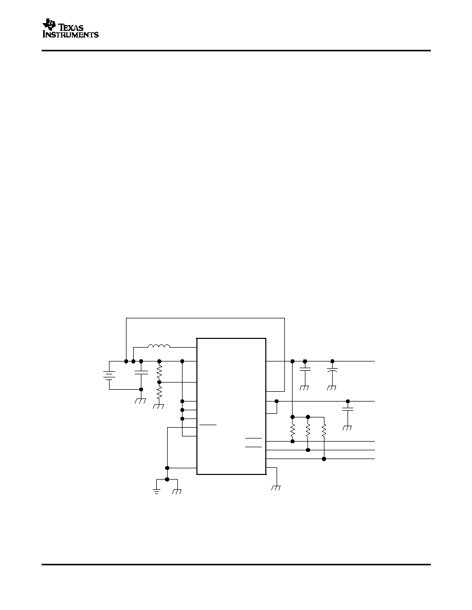
APPLICATION INFORMATION
DESIGN PROCEDURE
Programming the Output Voltage
R3
+
R6
V
O
V
FB
1
+
180 k
W
V
O
500 mV
1
(1)
SWN
C3
10
µ
F
Power
Supply
L1
10
µ
H
R1
R2
VBAT
VOUT
FB
R3
R6
LDOIN
R5
R4
LDOSENSE
LDOOUT
R7
R8
R9
C6
2.2
µ
F
C4
100
µ
F
U1
LBO1
LBO2
PGOOD
PGND
LBI
SKIPEN
ADEN
EN
ENPB
LDOEN
GND
TPS61100
V
CC1
Boost Output
V
CC2
LDO Output
Control
Outputs
C5
R5
+
R4
V
O
V
FB
1
+
180 k
W
V
O
500 mV
1
(2)
TPS61100, TPS61103
TPS61106, TPS61107
SLVS411B JUNE 2002 REVISED APRIL 2004
The TPS6110x boost converters are intended for systems powered by a single-cell NiCd or NiMH battery with a
typical terminal voltage between 0.9 V and 1.6 V. They can also be used in systems powered by two-cell NiCd or
NiMH batteries with a typical stack voltage between 1.8 V and 3.2 V. Additionally, single- or dual-cell, primary
and secondary alkaline battery cells can be the power source in systems where the TPS6110x is used.
Boost Converter
The output voltage of the TPS61100 boost converter section can be adjusted with an external resistor divider.
The typical value of the voltage on the FB pin is 500 mV. The maximum allowed value for the output voltage is
5.5 V. The current through the resistive divider should be about 100 times greater than the current into the FB
pin. The typical current into the FB pin is 0.01 µA and the voltage across R6 is typically 500 mV. Based on those
two values, the recommended value for R6 should be lower than 500 k
, in order to set the divider current at 1
µA or higher. Because of internal compensation circuitry the value for this resistor should be in the range of 200
k
. From that, the value of resistor R3, depending on the needed output voltage (V
O
), can be calculated using
Equation 1:
If as an example, an output voltage of 3.3 V is needed, a 1-M
resistor should be chosen for R3.
Figure 28. Typical Application Circuit for Adjustable Output Voltage Option
LDO
Programming the output voltage at the LDO follows almost the same rules as at the boost converter section. The
maximum programmable output voltage at the LDO is 3.3 V. Since reference and internal feedback circuitry are
similar, as they are at the boost converter section, R4 also should be in the 200-k
range. The calculation of the
value of R5 can be done using the following Equation 2:
If as an example, an output voltage of 1.5 V is needed, a 360 k
-resistor should be chosen for R5.
18

www.ti.com
Programming the LBI/LBO Threshold Voltage
R1
+
R2
V
BAT
V
LBI-threshold
1
+
390 k
W
V
BAT
450 mV
1
(3)
V
BAT
+
V
LBI-threshold
R1
R2
)
1
+
500 mV
680 k
W
390 k
W
)
1
(4)
Inductor Selection
I
L
+
I
OUT
V
OUT
V
BAT
0.8
(5)
TPS61100, TPS61103
TPS61106, TPS61107
SLVS411B JUNE 2002 REVISED APRIL 2004
APPLICATION INFORMATION (continued)
The current through the resistive divider should be about 100 times greater than the current into the LBI pin. The
typical current into the LBI pin is 0.01 µA, and the voltage across R2 is equal to the LBI voltage threshold that is
generated on-chip, which has a value of 400 mV, 450 mV or 500 mV. The recommended value for R2is therefore
in the range of 500 k
. From that, the value of resistor R
1
, depending on the desired minimum battery voltage
V
BAT,
can be calculated using Equation 3.
For example, if the low-battery detection circuit should flag an error condition for the 450 mV threshold on the
LBO outputs at a battery voltage of 1.23 V, a 680-k
resistor should be chosen for R1. The resulting battery
voltages of the other thresholds can be calculated using Equation 4:
The result for the 500-mV threshold in our example is 1.37 V and for the 400-mV threshold 1.1 V. This results in
the following truth table for the battery supervisor outputs:
VBAT [V]
LBO1
LBO2
0-1.1
0
0
1.1-1.23
1
0
1.23-1.37
0
1
1.37-VBAT max
1
1
If the application requires only a simple LBI/LBO function both LBO outputs can be connected together. The LBI
threshold then is 500 mV.
The outputs of the low battery supervisor are simple open-drain outputs that go active low if the dedicated battery
voltage drops below the programmed threshold voltage on LBI. The output requires a pullup resistor with a
recommended value of 1 M
. The maximum voltage which is used to pull up the LBO outputs should not exceed
the output voltage of the boost converter. If not used, the LBO pin can be left floating or tied to GND.
A boost converter normally requires two main passive components for storing energy during the conversion. A
boost inductor and a storage capacitor at the output are required. To select the boost inductor, it is
recommended to keep the possible peak inductor current below the current limit threshold of the power switch in
the chosen configuration. For example, the current limit threshold of the TPS6110x's switch is 1200 mA at an
output voltage of 3.3 V. The highest peak current through the inductor and the switch depends on the output
load, the input (V
BAT
), and the output voltage (V
OUT
). Estimation of the maximum average inductor current can be
done using Equation 5:
For example, for an output current of 100 mA at 3.3 V, at least 515 mA of current flows through the inductor at a
minimum input voltage of 0.8 V.
19

www.ti.com
L
+
V
BAT
V
OUT
V
BAT
D
I
L
V
OUT
(6)
CAPACITOR SELECTION
Input Capacitor
Output Capacitor Boost Converter
C
min
+
I
OUT
V
OUT
*
V
BAT
D
V
V
OUT
(7)
TPS61100, TPS61103
TPS61106, TPS61107
SLVS411B JUNE 2002 REVISED APRIL 2004
The second parameter for choosing the inductor is the desired current ripple in the inductor. Normally, it is
advisable to work with a ripple of less than 20% of the average inductor current. A smaller ripple reduces the
magnetic hysteresis losses in the inductor, as well as output voltage ripple and EMI. But in the same way,
regulation time at load changes rises. In addition, a larger inductor increases the total system costs. With those
parameters, it is possible to calculate the value for the inductor by using Equation 6:
Parameter 0 is the switching frequency and
I
L
is the ripple current in the inductor, i.e., 20%
×
I
L
. In this example,
the desired inductor has the value of 12 µH. With this calculated value and the calculated currents, it is possible
to choose a suitable inductor. Care has to be taken that load transients and losses in the circuit can lead to
higher currents as estimated in Equation 5. Also, the losses in the inductor caused by magnetic hysteresis losses
and copper losses are a major parameter for total circuit efficiency.
Table 1. Inductors
VENDOR
RECOMMENDED INDUCTOR SERIES
CDRH73
CDRH74
Sumida
CDRH5D18
CDRH6D38
DR73
Coiltronics
DR74
LQS66C
Murata
LQN6C
SLF 7045
TDK
SLF 7032
WE-PD Type M
Wurth Electronic
WE-PD Type S
At least a 10-µF input capacitor is recommended to improve transient behavior of the regulator and EMI behavior
of the total power supply circuit. A ceramic capacitor or a tantalum capacitor with a 100-nF ceramic capacitor in
parallel, placed close to the IC, is recommended.
The major parameter necessary to define the output capacitor is the maximum allowed output voltage ripple of
the converter. This ripple is determined by two parameters of the capacitor, the capacitance and the ESR. It is
possible to calculate the minimum capacitance needed for the defined ripple, supposing that the ESR is zero, by
using Equation 7:
Parameter f is the switching frequency and
V is the maximum allowed ripple.
20
www.ti.com
D
V
ESR
+
I
OUT
R
ESR
(8)
Output Capacitor LDO
LAYOUT CONSIDERATIONS
APPLICATION EXAMPLES
SWN
C3
10
µ
F
L1
10
µ
H
R1
R2
VBAT
VOUT
LDOIN
LDOSENSE
LDOOUT
R7
R8
R9
C6
2.2
µ
F
C4
100
µ
F
U1
LBO1
LBO2
PGOOD
PGND
LBI
SKIPEN
ADEN
EN
ENPB
LDOEN
GND
TPS61106
List of Components:
U1 = TPS61106
L1 = SUMIDA CDRH74100
C3, C5, C6 = X7R/X5R Ceramic
C4 = Low ESR Tantalum
3.3 V,
>250 mA
C5
2.2
µ
F
1.5 V,
>120 mA
LBO1
LBO2
PGOOD
TPS61100, TPS61103
TPS61106, TPS61107
SLVS411B JUNE 2002 REVISED APRIL 2004
With a chosen ripple voltage of 15 mV, a minimum capacitance of 10 µF is needed. The total ripple is larger due
to the ESR of the output capacitor. This additional component of the ripple can be calculated using Equation 8:
An additional ripple of 10 mV is the result of using a tantalum capacitor with a low ESR of 100 m
. The total
ripple is the sum of the ripple caused by the capacitance and the ripple caused by the ESR of the capacitor. In
this example, the total ripple is 25 mV. It is possible to improve the design by enlarging the capacitor or using
smaller capacitors in parallel to reduce the ESR or by using better capacitors with lower ESR, like ceramics. So,
trade-offs have to be made between performance and costs of the converter circuit.
To ensure stable output regulation, it is required to use an output capacitor at the LDO output. We recommend
using ceramic capacitors in the range from 1 µF up to 4.7 µF. At 4.7 µF and above it is recommended to use
standard ESR tantalum. There is no maximum capacitance value.
As for all switching power supplies, the layout is an important step in the design, especially at high peak currents
and high switching frequencies. If the layout is not carefully done, the regulator could show stability problems as
well as EMI problems. Therefore, use wide and short traces for the main current path and for the power ground
tracks. The input capacitor, output capacitor, and the inductor should be placed as close as possible to the IC.
Use a common ground node for power ground and a different one for control ground to minimize the effects of
ground noise. Connect these ground nodes at any place close to one of the ground pins of the IC.
The feedback divider should be placed as close as possible to the control ground pin of the IC. To lay out the
control ground, it is recommended to use short traces as well, separated from the power ground traces. This
avoids ground shift problems, which can occur due to superimposition of power ground current and control
ground current.
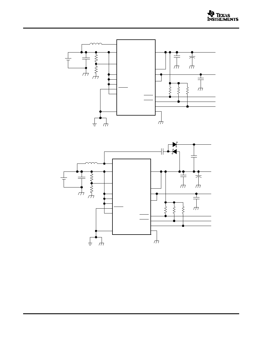
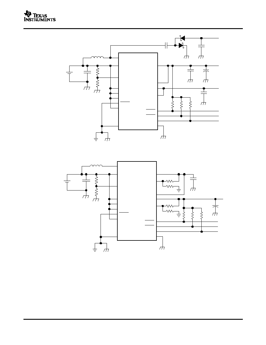
Figure 29. Solution for Maximum Output Power
21
www.ti.com
SWN
C3
10
µ
F
L1
10
µ
H
R1
R2
VBAT
VOUT
LDOIN
LDOSENSE
LDOOUT
R7
R8
R9
C6
2.2
µ
F
C4
100
µ
F
U1
LBO1
LBO2
PGOOD
PGND
LBI
SKIPEN
ADEN
EN
ENPB
LDOEN
GND
TPS61106
List of Components:
U1 = TPS61106
L1 = SUMIDA 5D18100
C3, C5, C6 = X7R/X5R Ceramic
C4 = Low ESR, Low Profile Tantalum
3.3 V
C5
2.2
µ
F
1.5 V
LBO1
LBO2
PGOOD
SWN
C3
10
µ
F
L1
10
µ
H
R1
R2
VBAT
VOUT
LDOIN
LDOSENSE
LDOOUT
R7
R8
R9
C6
2.2
µ
F
C4
100
µ
F
U1
LBO1
LBO2
PGOOD
PGND
LBI
SKIPEN
ADEN
EN
ENPB
LDOEN
GND
TPS61106
List of Components:
U1 = TPS61106
L1 = SUMIDA CDRH74100
C3, C5, C6,
C7, C8 = X7R/X5R Ceramic
C4 = Low ESR Tantalum
DS1 = BAT54S
3.3 V
C5
2.2
µ
F
1.5 V
LBO1
LBO2
PGOOD
C7
0.1
µ
F
DS1
C8
1
µ
F
6 V
TPS61100, TPS61103
TPS61106, TPS61107
SLVS411B JUNE 2002 REVISED APRIL 2004
Figure 30. Low Profile Solution, Maximum Height 1,8 mm
Figure 31. Dual Power Supply With Auxiliary Positive Output Voltage
22
www.ti.com
SWN
C3
10
µ
F
L1
10
µ
H
R1
R2
VBAT
VOUT
LDOIN
LDOSENSE
LDOOUT
R7
R8
R9
C6
2.2
µ
F
C4
100
µ
F
U1
LBO1
LBO2
PGOOD
PGND
LBI
SKIPEN
ADEN
EN
ENPB
LDOEN
GND
TPS61106
List of Components:
U1 = TPS61106
L1 = SUMIDA CDRH74100
C3, C5, C6,
C7, C8 = X7R/X5R Ceramic
C4 = Low ESR Tantalum
DS1 = BAT54S
3.3 V
C5
2.2
µ
F
1.5 V
LBO1
LBO2
PGOOD
C7
0.1
µ
F
DS1
C8
1
µ
F
3 V
SWN
C3
10
µ
F
L1
10
µ
H
R1
R2
VBAT
VOUT
FB
R3
R6
LDOIN
R5
R4
LDOSENSE
LDOOUT
R7
R8
R9
C6
22
µ
F
C5
2.2
µ
F
U1
LBO1
LBO2
PGOOD
PGND
LBI
SKIPEN
ADEN
EN
ENPB
LDOEN
GND
TPS61100
List of Components:
U1 = TPS61100
L1 = SUMIDA CDRH74100
C3, C5 = X7R/X5R Ceramic
C6 = X7R/X5R Ceramic or Low
ESR Tantalum
3.3 V
LBO1
LBO2
PGOOD
TPS61100, TPS61103
TPS61106, TPS61107
SLVS411B JUNE 2002 REVISED APRIL 2004
Figure 32. Dual Power Supply With Auxiliary Negative Output Voltage
Figure 33. Single Output Using LDO as Filter
23

www.ti.com
SWN
C3
10
µ
F
L1
10
µ
H
R1
R2
VBAT
VOUT
LDOIN
LDOSENSE
LDOOUT
R7
R8
R9
C6
2.2
µ
F
C4
100
µ
F
U1
LBO1
LBO2
PGOOD
PGND
LBI
SKIPEN
ADEN
EN
ENPB
LDOEN
GND
TPS61106
List of Components:
U1 = TPS61106
L1 = SUMIDA 5D18100
C3, C5, C6 = X7R/X5R Ceramic
C4 = Low ESR Tantalum
3.3 V
C5
2.2
µ
F
1.5 V
LBO1
LBO2
R10
SWN
C3
10
µ
F
USB-Input
4.2 V 5.5 V
L1
10
µ
H
R1
R2
VBAT
VOUT
FB
R3 1 M
R6
180 k
LDOIN
R5 1.022 M
R4
180 k
LDOSENSE
LDOOUT
R7
R8
R9
C6
2.2
µ
F
C4
100
µ
F
U1
LBO1
LBO2
PGOOD
PGND
LBI
SYNC
ADEN
EN
ENPB
LDOEN
GND
TPS61100
V
CC
3.3 V System
Supply
Control
Outputs
R10
680 k
R11
1 M
R12
180 k
D2
D1
List of Components:
U1 = TPS61100
L1 = SUMIDA CDRH73100
C3, C6 = X7R/X5R Ceramic
C4 = Low ESR Tantalum
D1 = ON-Semiconductor MBR0520
TPS61100, TPS61103
TPS61106, TPS61107
SLVS411B JUNE 2002 REVISED APRIL 2004
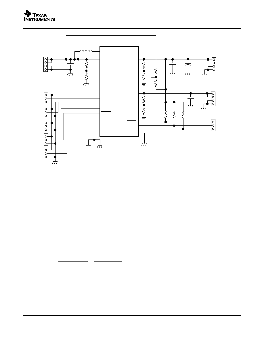
Figure 34. Simple Solution Using a Pushbutton for Start-Up
Figure 35. Dual Input Power Supply
24
www.ti.com
SWN
C3
10
µ
F
L1
10
µ
H
R1
R2
VBAT
VOUT
FB
LDOIN
LDOSENSE
LDOOUT
R7
R8
R9
C6
2.2
µ
F
C4
100
µ
F
U1
LBO1
LBO2
PGOOD
PGND
LBI
SKIPEN
ADEN
EN
ENPB
LDOEN
GND
TPS6110XRGE
C5
2.2
µ
F
R3
R6
R5
R4
LBO1
LBO2
PGOOD
LDOOUT
OUTPUT
LDOEN
ENPB
EN
ADEN
SKIPEN
INPUT
R11
R10
THERMAL INFORMATION
P
D(MAX)
+
T
J(MAX)
*
T
A
R
q
JA
+
150
°
C
*
85
°
C
155 k W
+
420 mW
(9)
TPS61100, TPS61103
TPS61106, TPS61107
SLVS411B JUNE 2002 REVISED APRIL 2004
Figure 36. TPS6110x EVM Circuit Diagram
Implementation of integrated circuits in low-profile and fine-pitch surface-mount packages typically requires
special attention to power dissipation. Many system-dependent issues such as thermal coupling, airflow, added
heat sinks and convection surfaces, and the presence of other heat-generating components affect the
power-dissipation limits of a given component.
Three basic approaches for enhancing thermal performance are listed below.
·
Improving the power dissipation capability of the PCB design.
·
Improving the thermal coupling of the component to the PCB.
·
Introducing airflow in the system.
The maximum junction temperature (T
J
) of the TPS6110x devices is 150
°
C. The thermal resistance of the 20-pin
TSSOP package (PW) isR
JA
= 155 K/W (QFN package, RGE, 161 K/W). Specified regulator operation is
assured to a maximum ambient temperature T
A
of 85
°
C. Therefore, the maximum power dissipation is about 420
mW. More power can be dissipated if the maximum ambient temperature of the application is lower.
25

MECHANICAL DATA
MTSS001C JANUARY 1995 REVISED FEBRUARY 1999
POST OFFICE BOX 655303
·
DALLAS, TEXAS 75265
PW (R-PDSO-G**)
PLASTIC SMALL-OUTLINE PACKAGE
14 PINS SHOWN
0,65
M
0,10
0,10
0,25
0,50
0,75
0,15 NOM
Gage Plane
28
9,80
9,60
24
7,90
7,70
20
16
6,60
6,40
4040064/F 01/97
0,30
6,60
6,20
8
0,19
4,30
4,50
7
0,15
14
A
1
1,20 MAX
14
5,10
4,90
8
3,10
2,90
A MAX
A MIN
DIM
PINS **
0,05
4,90
5,10
Seating Plane
0
°
8
°
NOTES: A. All linear dimensions are in millimeters.
B. This drawing is subject to change without notice.
C. Body dimensions do not include mold flash or protrusion not to exceed 0,15.
D. Falls within JEDEC MO-153

IMPORTANT NOTICE
Texas Instruments Incorporated and its subsidiaries (TI) reserve the right to make corrections, modifications,
enhancements, improvements, and other changes to its products and services at any time and to discontinue
any product or service without notice. Customers should obtain the latest relevant information before placing
orders and should verify that such information is current and complete. All products are sold subject to TI's terms
and conditions of sale supplied at the time of order acknowledgment.
TI warrants performance of its hardware products to the specifications applicable at the time of sale in
accordance with TI's standard warranty. Testing and other quality control techniques are used to the extent TI
deems necessary to support this warranty. Except where mandated by government requirements, testing of all
parameters of each product is not necessarily performed.
TI assumes no liability for applications assistance or customer product design. Customers are responsible for
their products and applications using TI components. To minimize the risks associated with customer products
and applications, customers should provide adequate design and operating safeguards.
TI does not warrant or represent that any license, either express or implied, is granted under any TI patent right,
copyright, mask work right, or other TI intellectual property right relating to any combination, machine, or process
in which TI products or services are used. Information published by TI regarding third-party products or services
does not constitute a license from TI to use such products or services or a warranty or endorsement thereof.
Use of such information may require a license from a third party under the patents or other intellectual property
of the third party, or a license from TI under the patents or other intellectual property of TI.
Reproduction of information in TI data books or data sheets is permissible only if reproduction is without
alteration and is accompanied by all associated warranties, conditions, limitations, and notices. Reproduction
of this information with alteration is an unfair and deceptive business practice. TI is not responsible or liable for
such altered documentation.
Resale of TI products or services with statements different from or beyond the parameters stated by TI for that
product or service voids all express and any implied warranties for the associated TI product or service and
is an unfair and deceptive business practice. TI is not responsible or liable for any such statements.
Following are URLs where you can obtain information on other Texas Instruments products and application
solutions:
Products
Applications
Amplifiers
amplifier.ti.com
Audio
www.ti.com/audio
Data Converters
dataconverter.ti.com
Automotive
www.ti.com/automotive
DSP
dsp.ti.com
Broadband
www.ti.com/broadband
Interface
interface.ti.com
Digital Control
www.ti.com/digitalcontrol
Logic
logic.ti.com
Military
www.ti.com/military
Power Mgmt
power.ti.com
Optical Networking
www.ti.com/opticalnetwork
Microcontrollers
microcontroller.ti.com
Security
www.ti.com/security
Telephony
www.ti.com/telephony
Video & Imaging
www.ti.com/video
Wireless
www.ti.com/wireless
Mailing Address:
Texas Instruments
Post Office Box 655303 Dallas, Texas 75265
Copyright
2004, Texas Instruments Incorporated