
TPS2838, TPS2839
TPS2848, TPS2849
SLVS367A ş MARCH 2001 ş REVISED JUNE 2001
SYNCHRONOUS BUCK MOSFET DRIVERS
WITH DRIVE REGULATOR
1
www.ti.com
FEATURES
D
Integrated Drive Regulator (4 V to 14 V)
D
Adjustable/Adaptive Dead-Time Control
D
4-A Peak current at VDRV of 14 V
D
10-V to 15-V Supply Voltage Range
D
TTL-Compatible Inputs
D
Internal Schottky Diode Reduces Part Count
D
Synchronous or Nonsynchronous Operation
D
Inverting and Noninverting Options
D
TSSOP PowerPad
Package for Excellent
Thermal Performance
APPLICATIONS
D
Single or Multiphase Synchronous-Buck
Power Supplies
D
High-Current DC/DC Power Modules
DESCRIPTION
The TPS2838/39/48/49 devices are MOSFET
drivers designed for high-performance
synchronous power supplies. The drivers can
source and sink up to 4-A peak current at a 14-V
drive voltage. These are ideal devices to use with
power supply controllers that do not have on-chip
drivers. The low-side driver is capable of driving
loads of 3.3 nF in 10-ns rise/fall times and has
40-ns propagation delays at room temperature.
The MOSFET drivers have an integrated 150-mA
regulator, so the gate drive voltage can be
optimized for specific MOSFETs. The TPS2848
and TPS2849 have a fixed 8-V drive regulator,
while the TPS2838/39 allow the drive regulator to
be adjusted from 4 V to 14 V by selection of two
external resistors.
The devices feature VDRV to PGND shoot-
through protection with adaptive/adjustable
deadtime control. The deadtime, for turning on the
high-side FET from LOWDR transitioning low, is
adjustable with an external capacitor on the
DELAY pin. This allows compensation for the
effect the gate resistor has on the synchronous
FET turn off. The adaptive deadtime prevents the
turning on of the low-side FET until the voltage on
the BOOTLO pin falls below a threshold after the
high-side FET stops conducting. The high-side
drive can be configured as a ground referenced
driver or a floating bootstrap driver. The internal
Schottky diode minimizes the size and number of
external components needed for the bootstrap
driver circuit. Only one external ceramic capacitor
is required to configure the bootstrap driver.
1
2
3
4
5
6
7
14
13
12
11
10
9
8
ENABLE
IN
PWRRDY
DELAY
NC
DT
AGND
BOOT
HIGHDR
BOOTLO
V
CC
VDRV
LOWDR
PGND
Thermal
Pad
TPS2848, TPS2849
PWP PACKAGE
(TOP VIEW)
1
2
3
4
5
6
7
8
16
15
14
13
12
11
10
9
ENABLE
IN
PWRRDY
DELAY
SYNC
ADJ
DT
AGND
BOOT
HIGHDR
BOOTLO
V
CC
VDRV
LOWDR
NC
PGND
Thermal
Pad
TPS2838, TPS2839
PWP PACKAGE
(TOP VIEW)
ACTUAL SIZE
(5,1 mm x 6,6 mm)
ACTUAL SIZE
(5,1 mm x 6,6 mm)
PRODUCTION DATA information is current as of publication date.
Products conform to specifications per the terms of Texas Instruments
standard warranty. Production processing does not necessarily include
testing of all parameters.
Copyright
2001, Texas Instruments Incorporated
PowerPAD is a trademark of Texas Instruments.
Please be aware that an important notice concerning availability, standard warranty, and use in critical applications of
Texas Instruments semiconductor products and disclaimers thereto appears at the end of this data sheet.

TPS2838, TPS2839
TPS2848, TPS2849
SLVS367A ş MARCH 2001 ş REVISED JUNE 2001
2
www.ti.com
description (continued)
The SYNC pin can be used regardless of load to disable the synchronous FET driver and operate the power
supply nonsynchronously.
A power ready/undervoltage lockout function outputs the status of the V
CC
-pin voltage and driver regulator
output on the open-drain PWRRDY pin. This feature can be used to enable a controller's output once the V
CC
voltage reaches the threshold and the regulator output is stable. This function ensures both FET drivers are off
when the V
CC
voltage is below the voltage threshold.
The TPS2838/39/48/49 devices are offered in the thermally enhanced 14-pin and 16-pin PowerPAD TSSOP
package. The PowerPAD package features an exposed leadframe on the bottom that can be soldered to the
printed-circuit board to improve thermal efficiency. The TPS2838/48 are noninverting control logic while the
TPS2839/49 drivers are inverting control logic.
TPS2838, TPS2839
TPS2848, TPS2849
SLVS367A ş MARCH 2001 ş REVISED JUNE 2001
3
www.ti.com
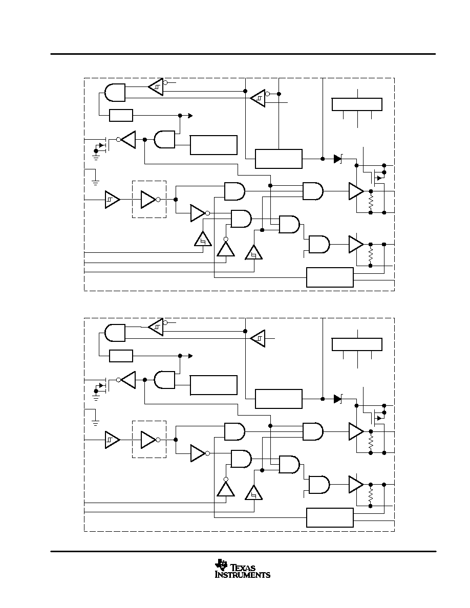
functional block diagram (TPS2838, TPS2839)
POR
Vr1
PWRRDY
THERMAL
SHUTDOWN
SYS_UVLO
VCC
DRIVE
REGULATOR
REFERENCES
VCC
Vr1
Vref
0.9
Î
Vref
VDRV
ADJ
SHUTDOWN
BOOT
0.9
Î
Vref
AGND
BOOTLO
HIGHDR
SHUTDOWN
INVERTING OPTION
TPS2839 ONLY
PGND
LOWDR
SYS_UVLO
VDRV
DEADTIME
CONTROL
DELAY
SYNC
DT
ENABLE
IN
functional block diagram (TPS2848, TPS2849)
POR
Vr1
PWRRDY
THERMAL
SHUTDOWN
SYS_UVLO
VCC
DRIVE
REGULATOR
REFERENCES
VCC
Vr1
Vref
0.9
Î
Vref
VDRV
SHUTDOWN
BOOT
0.9
Î
Vref
AGND
BOOTLO
HIGHDR
SHUTDOWN
INVERTING OPTION
TPS2849 ONLY
PGND
LOWDR
SYS_UVLO
VDRV
DEADTIME
CONTROL
DELAY
DT
ENABLE
IN
TPS2838, TPS2839
TPS2848, TPS2849
SLVS367A ş MARCH 2001 ş REVISED JUNE 2001
4
www.ti.com
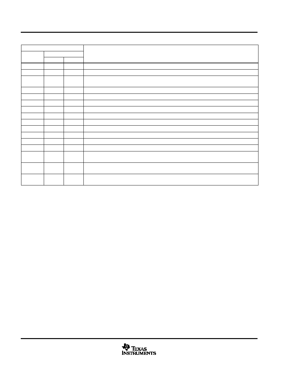
Terminal Functions
TERMINAL
NAME
NO.
DESCRIPTION
NAME
TPS283x
TPS284x
DESCRIPTION
ADJ
6
--
Adjust. The adjust pin is the feedback pin for the drive regulator (TPS283X only)
AGND
8
7
Analog ground
BOOT
16
14
Bootstrap. A capacitor is connected between the BOOT and BOOTLO pins to develop the floating
bootstrap voltage for the high-side MOSFET. The capacitor value is typically between 0.1
Á
F and 1
Á
F.
BOOTLO
14
12
Boot low. This pin connects to the junction of the high-side and low-side MOSFETs.
DELAY
4
4
Delay. Connecting a capacitor between this pin and ground adjusts the deadtime for high-side driver
DT
7
6
Deadtime control. Connect DT to the junction of the high-side and low-side MOSFETs
ENABLE
1
1
Enable. If ENABLE is low, both drivers are off.
HIGHDR
15
13
High drive. This pin is the output drive for the high-side power MOSFET.
IN
2
2
Input. This pin is the input signal to the MOSFET drivers.
LOWDR
11
9
Low drive. This pin is the output drive for the low-side power MOSFET.
NC
10
5
No internal connection
PGND
9
8
Power ground. This pin is connected to the FET power ground.
PWRRDY
3
3
Power ready. This open-drain pin indicates a power good for VDRV and VCC.
SYNC
5
--
Synchronous rectifier enable. If SYNC is low, the low-side driver is always off; if SYNC is high, the
low-side driver provides gate drive to the low-side MOSFET.
VCC
13
11
Input power supply. It is recommended that a capacitor (minimum 1
Á
F) be connected from VCC to
PGND. Note that VCC must be 2 V higher than VDRV.
VDRV
12
10
Drive regulator output voltage. It is recommended that a capacitor (minimum 1
Á
F) be connected from
VDRV to PGND. Note that VCC must be 2 V higher than VDRV.
detailed description
low-side driver
The low-side driver is designed to drive low r
DS(on)
N-channel MOSFETs. The current rating of the driver is 4 A,
source and sink.
high-side driver
The high-side driver is designed to drive low r
DS(on)
N-channel MOSFETs. The current rating of the driver is 4 A
minimum, source and sink. The high-side driver can be configured as a GND-reference driver or as a
floating-bootstrap driver. The internal bootstrap diode is a Schottky, for improved drive efficiency. The maximum
voltage that can be applied from BOOT to ground is 30 V.
dead-time (DT) control
Dead-time control prevents shoot-through current from flowing through the main power FETs during switching
transitions by controlling the turnon times of the MOSFET drivers. The high-side driver is not allowed to turn
on until the gate drive voltage to the low-side FET is low, and the low-side driver is not allowed to turn on until
the voltage at the junction of the power FETs (BOOTLO) is low. The TTL-compatible DT terminal connects to
the junction of the power FETs.
ENABLE
The ENABLE terminal enables the drivers. When enable is low, the output drivers are low. ENABLE is a
TTL-compatible digital terminal.

TPS2838, TPS2839
TPS2848, TPS2849
SLVS367A ş MARCH 2001 ş REVISED JUNE 2001
5
www.ti.com
detailed description (continued)
IN
The IN terminal is a TTL-compatible digital terminal that is the input control signal for the drivers. The
TPS2838/48 have noninverting inputs; the TPS2839/49 have inverting inputs. On the TPS2838 and TPS2848,
a high on IN results in a high on HIGHDR. On the TPS2839 and TPS2849, a high on IN results in a low on
HIGHDR.
SYNC (TPS283x only)
The SYNC terminal controls whether the drivers operate in synchronous or nonsynchronous mode. In
synchronous mode, the low-side FET is operated as a synchronous rectifier. In nonsynchronous mode, the
low-side FET is always off. SYNC is a TTL-compatible digital terminal.
PWRRDY
Depicts the status of the V
CC
pin voltage and the driver regulator output on the open-drain PWRRDY pin.
DELAY
Adjustable high-side turnon delay from from when the low-side FET is turned off.
ADJ (TPS283x only)
Input for adjusting the driver regulator output. See the application information section for the adjustment formula.
absolute maximum ratings over operating free-air temperature (unless otherwise noted)
Supply voltage range, V
CC
(see Note 1)
ş0.3 V to 16 V
. . . . . . . . . . . . . . . . . . . . . . . . . . . . . . . . . . . . . . . . . . . . . .
Input voltage range: ADJ
ş0.3 V to 7 V
. . . . . . . . . . . . . . . . . . . . . . . . . . . . . . . . . . . . . . . . . . . . . . . . . . . . . . . . . . . .
BOOT to PGND (high-side driver ON)
ş0.3 V to 30 V
. . . . . . . . . . . . . . . . . . . . . . . . . . . . . .
BOOTLO to PGND
ş0.3 V to 16 V
. . . . . . . . . . . . . . . . . . . . . . . . . . . . . . . . . . . . . . . . . . . . . .
BOOT to BOOTLO
ş0.3 V to 16 V
. . . . . . . . . . . . . . . . . . . . . . . . . . . . . . . . . . . . . . . . . . . . . .
ENABLE, IN, and SYNC
ş0.3 V to 16 V
. . . . . . . . . . . . . . . . . . . . . . . . . . . . . . . . . . . . . . . . . .
VDRV, PWRRDY, and DELAY
ş0.3 V to 16 V
. . . . . . . . . . . . . . . . . . . . . . . . . . . . . . . . . . . . .
DT
ş0.3 V to 16 V
. . . . . . . . . . . . . . . . . . . . . . . . . . . . . . . . . . . . . . . . . . . . . . . . . . . . . . . . . . . . .
Continuous total power dissipation
See Dissipation Rating Table
. . . . . . . . . . . . . . . . . . . . . . . . . . . . . . . . . . . . . .
Operating virtual junction temperature range, T
J
ş40
░
C to 125
░
C
. . . . . . . . . . . . . . . . . . . . . . . . . . . . . . . . . . . . . .
Storage temperature range, T
stg
ş65
░
C to 150
░
C
. . . . . . . . . . . . . . . . . . . . . . . . . . . . . . . . . . . . . . . . . . . . . . . . . . . .
Lead temperature soldering 1,6 mm (1/16 inch) from case for 10 seconds
260
░
C
. . . . . . . . . . . . . . . . . . . . . . .
Stresses beyond those listed under "absolute maximum ratings" may cause permanent damage to the device. These are stress ratings only, and
functional operation of the device at these or any other conditions beyond those indicated under "recommended operating conditions" is not
implied. Exposure to absolute-maximum-rated conditions for extended periods may affect device reliability.
NOTE 1: Unless otherwise specified, all voltages are with respect to PGND.