TPPM0304
250-mA LOW-DROPOUT REGULATOR
WITH AUXILIARY POWER MANAGEMENT
SLVS320 OCTOBER 2000
1
POST OFFICE BOX 655303
·
DALLAS, TEXAS 75265
D
Automatic Input Voltage Source Selection
D
Glitch-Free Regulated Output
D
5-V Input Voltage Source Detector With
Hysteresis
D
250-mA Load Current Capability With 5-V or
3.3-V Input Source
D
Low r
DS(on)
Auxiliary Switch
description
The TPPM0304 is a low-dropout regulator with
auxiliary power management that provides a
constant 3.3-V supply at the output capable of
driving a 250-mA load.
The TPPM0304 provides a regulated power output for systems that have multiple input sources and require a
constant voltage source with a low-dropout voltage. This is a single output, multiple input, intelligent power
source selection device with a low-dropout regulator for either 5VCC or 5VAUX inputs, and a low- resistance
bypass switch for the 3.3VAUX input.
Transitions may occur from one input supply to another without generating a glitch, outside of the specification
range, on the 3.3-V output. The device has an incorporated reverse blocking scheme to prevent excess leakage
from the input terminals in the event that the output voltage is greater than the input voltage.
The input voltage is prioritized in the following order: 5VCC, 5VAUX, and 3.3VAUX.
Copyright
©
2000, Texas Instruments Incorporated
PRODUCTION DATA information is current as of publication date.
Products conform to specifications per the terms of Texas Instruments
standard warranty. Production processing does not necessarily include
testing of all parameters.
Please be aware that an important notice concerning availability, standard warranty, and use in critical applications of
Texas Instruments semiconductor products and disclaimers thereto appears at the end of this data sheet.
1
2
3
4
8
7
6
5
GND
5VAUX
NC
5VCC
NC
3.3VAUX
NC
3.3VOUT
D PACKAGE
(TOP VIEW)
NC No internal connection
This package is available taped and reeled. To
order this packaging option, add an R suffix to
the part number (e.g., TPPM0304DR).
TPPM0304
250-mA LOW-DROPOUT REGULATOR
WITH AUXILIARY POWER MANAGEMENT
SLVS320 OCTOBER 2000
2
POST OFFICE BOX 655303
·
DALLAS, TEXAS 75265
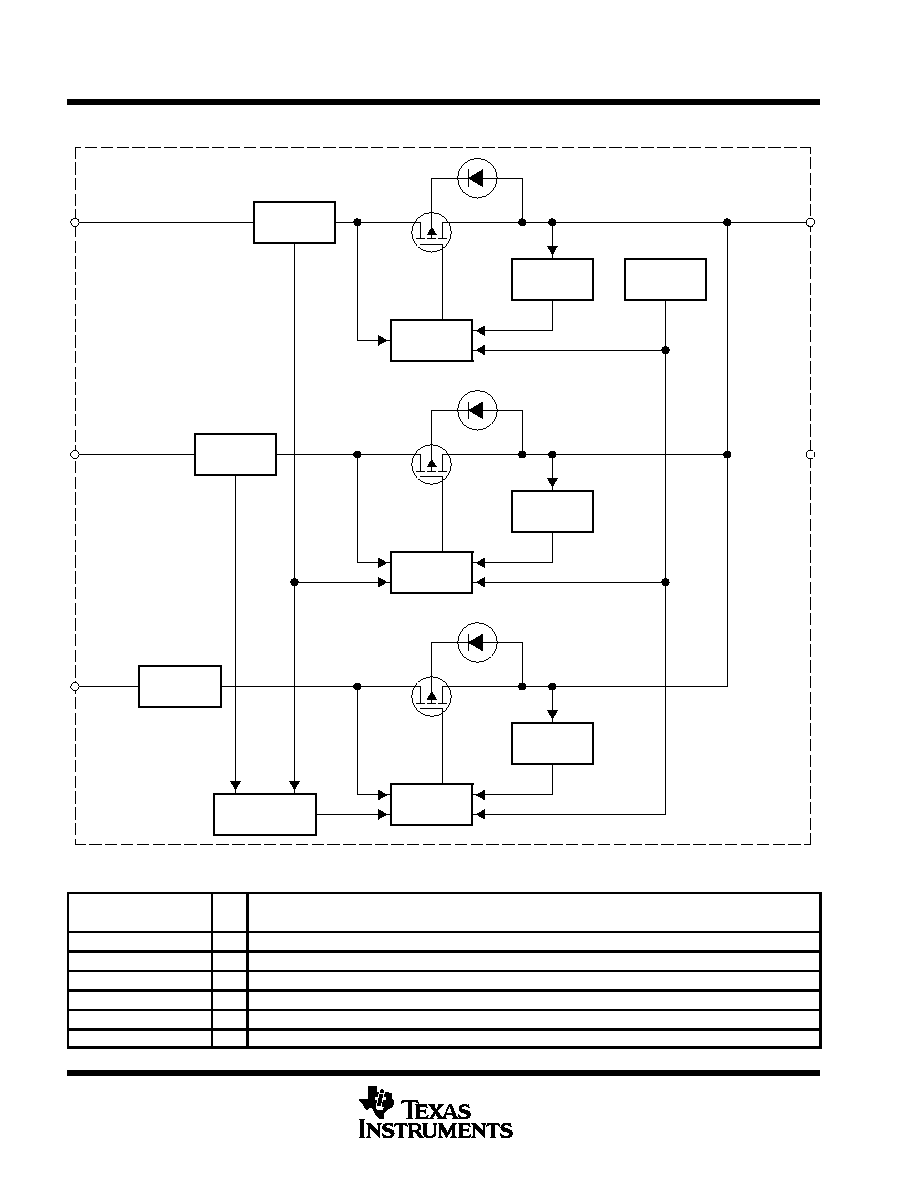
functional block diagram
5VCC
5-V
Detection
Current
Sensor
Linear Regulator
With LDO
Gate Drive
and Control
Over
Temperature
3.3VOUT
5VAUX
5VAUX
Detection
Current
Sensor
Gate Drive
and Control
GND
3.3VAUX
3VAUX
Detection
Current
Sensor
Low ON
Resistance
Switch
Gate Drive
5-V Detection
and Control
Linear Regulator
With LDO
Terminal Functions
TERMINAL
I/O
DESCRIPTION
NAME
NO.
I/O
DESCRIPTION
3.3VAUX
7
I
3.3-V auxiliary input
3.3VOUT
5
O
3.3-V output with a typical capacitance load of 4.7
µ
F
5VAUX
2
I
5-V auxiliary input
5VCC
4
I
5-V main input
GND
1
I
Ground
NC
3, 6, 8
I/O
No internal connection

TPPM0304
250-mA LOW-DROPOUT REGULATOR
WITH AUXILIARY POWER MANAGEMENT
SLVS320 OCTOBER 2000
3
POST OFFICE BOX 655303
·
DALLAS, TEXAS 75265
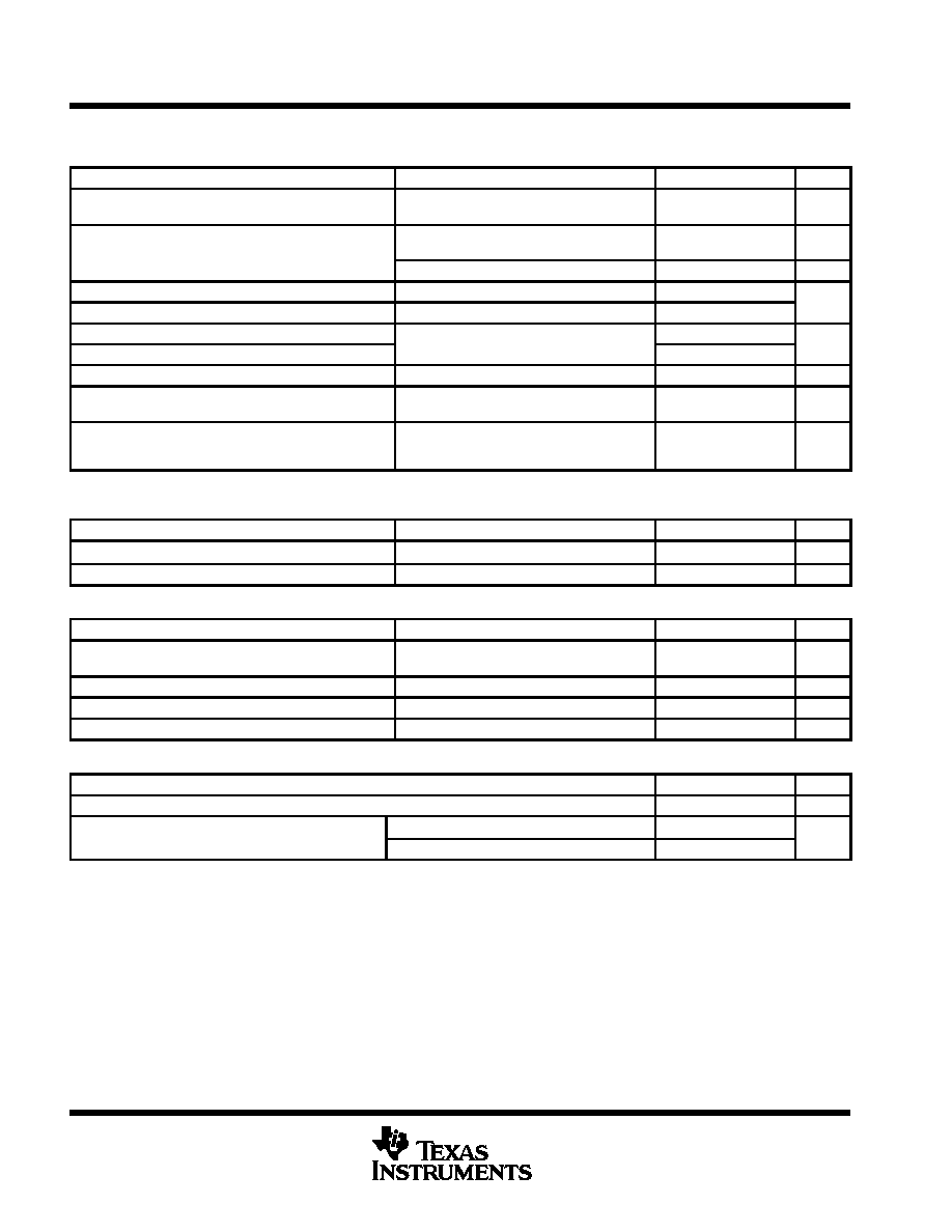
Table 1. Input Selection
INPUT VOLTAGE STATUS
(V)
INPUT SELECTED
OUTPUT
(V)
OUTPUT
(I)
5VCC
5VAUX
3.3VAUX
5VCC/5VAUX/3.3VAUX
3.3VOUT
IL (mA)
0
0
0
None
0
0
0
0
3.3
3.3VAUX
3.3
250
0
5
0
5VAUX
3.3
250
0
5
3.3
5VAUX
3.3
250
5
0
0
5VCC
3.3
250
5
0
3.3
5VCC
3.3
250
5
5
0
5VCC
3.3
250
5
5
3.3
5VCC
3.3
250
absolute maximum ratings over operating free-air temperature (unless otherwise noted)
Supply voltage, 5-V main input, V
(5VCC)
(see Notes 1 and 2)
7 V
. . . . . . . . . . . . . . . . . . . . . . . . . . . . . . . . . . . . .
Auxiliary voltage, 5-V input, V
(5VAUX)
(see Notes 1 and 2)
7 V
. . . . . . . . . . . . . . . . . . . . . . . . . . . . . . . . . . . . . . .
Auxiliary voltage, 3.3-V input, V
(3.3VAUX)
(see Notes 1 and 2)
5 V
. . . . . . . . . . . . . . . . . . . . . . . . . . . . . . . . . . . .
3.3-V output current limit, I
(LIMIT)
1.5
A
. . . . . . . . . . . . . . . . . . . . . . . . . . . . . . . . . . . . . . . . . . . . . . . . . . . . . . . . . . .
Continuous power dissipation (low-K), P
D
(see Note 3)
0.625 W
. . . . . . . . . . . . . . . . . . . . . . . . . . . . . . . . . . . . . .
Electrostatic discharge susceptibility, human body model, V
(HBMESD)
2
kV
. . . . . . . . . . . . . . . . . . . . . . . . . . . .
Operating ambient temperature range, T
A
0
°
C to 70
°
C
. . . . . . . . . . . . . . . . . . . . . . . . . . . . . . . . . . . . . . . . . . . . . .
Storage temperature range, T
stg
55
°
C to 150
°
C
. . . . . . . . . . . . . . . . . . . . . . . . . . . . . . . . . . . . . . . . . . . . . . . . . . .
Operating junction temperature range, T
J
5
°
C to 120
°
C
. . . . . . . . . . . . . . . . . . . . . . . . . . . . . . . . . . . . . . . . . . . .
Lead temperature (soldering, 10 second), T
(LEAD)
260
°
C
. . . . . . . . . . . . . . . . . . . . . . . . . . . . . . . . . . . . . . . . . . .
Stresses beyond those listed under "absolute maximum ratings" may cause permanent damage to the device. These are stress ratings only, and
functional operation of the device at these or any other conditions beyond those indicated under "recommended operating conditions" is not
implied. Exposure to absolute-maximum-rated conditions for extended periods may affect device reliability.
NOTES:
1. All voltage values are with respect to GND.
2. Absolute negative voltage on these terminal should not be below 0.5 V.
3. The device derates with increase in ambient temperature, TA. See Thermal Information section.
recommended operating conditions
MIN
TYP
MAX
UNIT
5-V main input, V(5VCC)
4.5
5.5
V
5-V auxiliary input, V(5VAUX)
4.5
5.5
V
3.3-V auxiliary input, V(3.3VAUX)
3
3.6
V
Load capacitance, CL
4.23
4.7
5.17
µ
F
Load current, IL
0
250
mA
Ambient temperature, TA
0
70
°
C
TPPM0304
250-mA LOW-DROPOUT REGULATOR
WITH AUXILIARY POWER MANAGEMENT
SLVS320 OCTOBER 2000
4
POST OFFICE BOX 655303
·
DALLAS, TEXAS 75265
electrical characteristics over recommended operating free-air temperature range, T
A
= 0
°
C to
70
°
C, C
L
= 4.7
µ
F (unless otherwise noted)
PARAMETER
TEST CONDITIONS
MIN
TYP
MAX
UNIT
V(5VCC)/
V(5VAUX)
5-V inputs
4.5
5
5.5
V
I(Q)
Quiescent supply current
From 5VCC or 5VAUX terminals, IL = 0 to
250 mA
2.5
5
mA
(Q)
y
From 3.3VAUX terminal, IL = 0 A
250
500
µ
A
IL
Output load current
0.25
A
I(LIMIT)
Output current limit
3.3VOUT = 0 V
2
A
T(TSD)
Thermal shutdown
3 3VOUT output shorted to 0 V
150
180
°
C
Thys
Thermal hysteresis
3.3VOUT output shorted to 0 V
15
°
C
V(3.3VOUT)
3.3-V output
IL = 250 mA
3.135
3.3
3.465
V
CL
Load capacitance
Minimal ESR to insure stability of regulated
output
4.7
µ
F
Ilkg(REV)
Reverse leakage output current
Tested for input that is grounded.
3.3VAUX, 5VAUX or 5VCC = GND,
3.3VOUT = 3.3 V
50
µ
A
Design targets only. Not tested in production.
5-V detect
PARAMETER
TEST CONDITIONS
MIN
TYP
MAX
UNIT
V(TO_LO)
Threshold voltage, low
5VAUX or 5VCC
3.85
4.05
4.25
V
V(TO_HI)
Threshold voltage, high
5VAUX or 5VCC
4.1
4.3
4.5
V
auxiliary switch
PARAMETER
TEST CONDITIONS
MIN
TYP
MAX
UNIT
R(SWITCH)
Auxiliary switch resistance
5VAUX = 5VCC = 0 V,
3.3VAUX = 3.3 V, IL = 150 mA
0.4
VO(
VI)
Line regulation voltage
5VAUX or 5VCC = 4.5 V to 5.5 V
2
mV
VO(
IO)
Load regulation voltage
20 mA < IL < 250 mA
40
mV
VI VO
Dropout voltage
IL < 250 mA
1
V
thermal characteristics
PARAMETER
MIN
TYP
MAX
UNIT
R
JC
Thermal impedance, junction-to-case
39
°
C/W
R
JA
Thermal impedance junction-to-ambient
Low-K (see Note 4)
176
°
C/W
R
JA
Thermal im edance, junction-to-ambient
High-K (see Note 4)
98
°
C/W
NOTE 4: See JEDEC PCB specifications for low-K and high-K.
TPPM0304
250-mA LOW-DROPOUT REGULATOR
WITH AUXILIARY POWER MANAGEMENT
SLVS320 OCTOBER 2000
5
POST OFFICE BOX 655303
·
DALLAS, TEXAS 75265
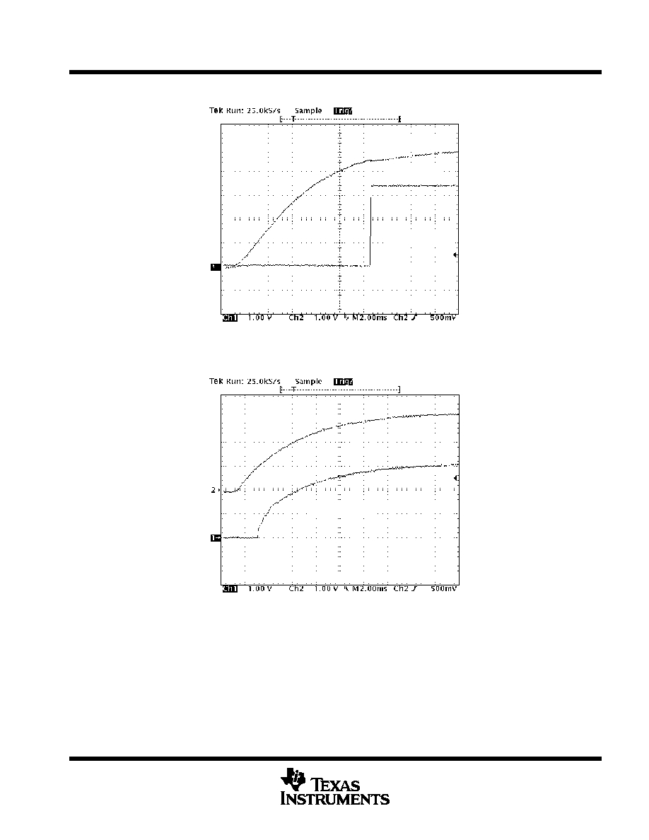
TYPICAL CHARACTERISTICS
5VCC
3.3VOUT
(250mA load)
Figure 1. 5VCC Cold Start
3.3VAUX
3.3VOUT
(250mA load)
Figure 2. 3.3VAUX Cold Start