
TPPM0125
150-mA LOW DROPOUT REGULATOR WITH POK
SLVS388 ¡ JULY 2001
1
POST OFFICE BOX 655303
À
DALLAS, TEXAS 75265
features
D
Low Dropout Voltage Regulator, 1.2-V
D
150-mA Load Current Capability
D
Power Okay (POK) Function
D
Load Independent, Low Ground
Current,150-
Á
A
D
Current Limiting
D
Thermal Shutdown
D
Low Sleep State Current (Off Mode)
D
Fast Transient Response
D
Low Variation Due to Load and Line
Regulation
D
Output Stable With Low ESR Capacitors
D
TTL Logic Controlled Enable Input
applications
D
Processor Powerup Sequencing
D
Palmtop Computers, Laptops, and
Notebooks
description
The TPPM0125 is a low dropout voltage regulator with an output tolerance of
▒
2% over the operating range.
The device is optimized for low noise applications and has a low quiescent current (enable <0.8 V). The device
has a low dropout voltage at full load (150 mA). The power okay function monitors the output voltage and
indicates when an error occurs in the system (active low). In the event of an output fault such as overcurrent,
thermal shutdown, or dropout, the power okay output is pulled low (open drain).
The TPPM0125 has a fast transient response recovery capability in the event of load transition from heavy load
to light load. The device also minimizes overshoot during this condition. During power down, the output
capacitor and load are de-energized through the internal active shutdown clamp, which is turned on when the
device is disabled.
The TPPM0125 requires a small output capacitor for stability with low ESR. An input capacitor is not required
unless the bulk ac capacitor is placed away from the device or the power supply is a battery. In this situation,
a 1-
Á
F capacitor is recommended for the application. Low ESR ceramic capacitors may be used with the device
to reduce board space in power applications, a key concern in hand-held wireless devices.
Copyright
2001, Texas Instruments Incorporated
Please be aware that an important notice concerning availability, standard warranty, and use in critical applications of
Texas Instruments semiconductor products and disclaimers thereto appears at the end of this data sheet.
3
2
4
5
DBV PACKAGE
(TOP VIEW)
1
V
I
GND
EN
V
O
POK
PRODUCTION DATA information is current as of publication date.
Products conform to specifications per the terms of Texas Instruments
standard warranty. Production processing does not necessarily include
testing of all parameters.
TPPM0125
150-mA LOW DROPOUT REGULATOR WITH POK
SLVS388 ¡ JULY 2001
2
POST OFFICE BOX 655303
À
DALLAS, TEXAS 75265
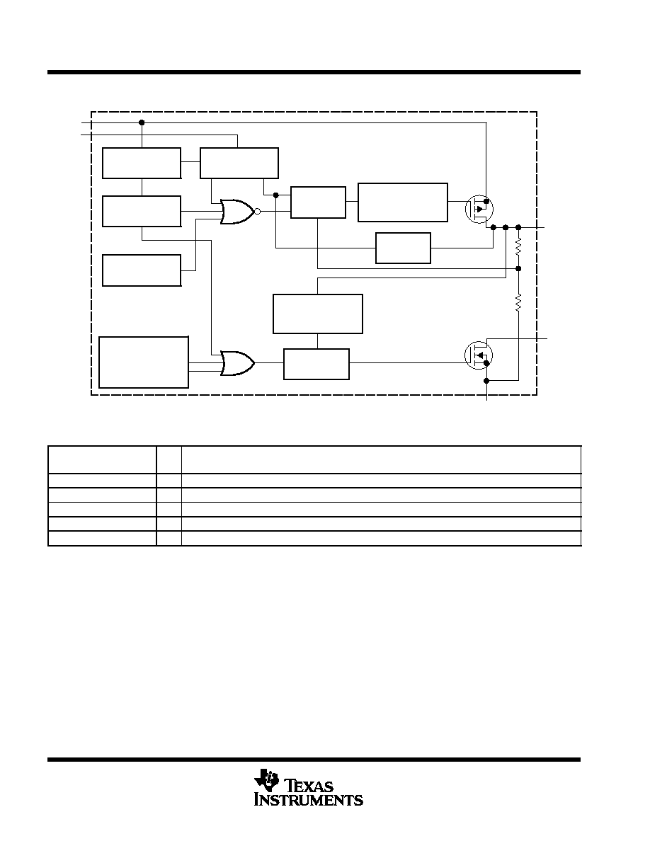
functional block diagram
Enable/Disable
Control
Voltage
Reference
Thermal
Sensor
Undervoltage
Lockout
Error
Amplifier
Gate Drive Control
and
Current Amplifier
Active
Shutdown
Voltage Supervisor
With
Delay Timer
Power Okay
Control
Overcurrent
Detection and
Dropout Voltage
Detection
Fault
Fault
VI
EN
VO
POK
GND
Terminal Functions
TERMINAL
I/O
DESCRIPTION
NAME
NO.
I/O
DESCRIPTION
EN
3
I
Enable/shutdown input (active high)
GND
2
I
Ground
POK
4
I
Power okay indicator
VI
1
I
Input supply voltage
VO
5
O
Output voltage
TPPM0125
150-mA LOW DROPOUT REGULATOR WITH POK
SLVS388 ¡ JULY 2001
3
POST OFFICE BOX 655303
À
DALLAS, TEXAS 75265
absolute maximum ratings over operating free-air temperature (unless otherwise noted)
Main input voltage range, V
I
(see Notes 1 and 2)
0 V to 7 V
. . . . . . . . . . . . . . . . . . . . . . . . . . . . . . . . . . . . . . . . . .
Enable input voltage range, V
(EN)
(see Notes 1 and 2)
0 V ¡ V
I
. . . . . . . . . . . . . . . . . . . . . . . . . . . . . . . . . . . . . .
Power okay output voltage range V
(POK)
, (see Notes 1 and 2)
0 V ¡ V
I
. . . . . . . . . . . . . . . . . . . . . . . . . . . . . . . .
Regulated output current limit, I
O
400
mA
. . . . . . . . . . . . . . . . . . . . . . . . . . . . . . . . . . . . . . . . . . . . . . . . . . . . . . . . .
Continuous power dissipation, P
D,
T
A
= 25
░
C
0.5 W
. . . . . . . . . . . . . . . . . . . . . . . . . . . . . . . . . . . . . . . . . . . . . . . .
Electrostatic discharge susceptibility, V
(HBMESD)
, (see Note 3)
2 kV
. . . . . . . . . . . . . . . . . . . . . . . . . . . . . . . . . .
Junction temperature, T
J
,
150
░
C
. . . . . . . . . . . . . . . . . . . . . . . . . . . . . . . . . . . . . . . . . . . . . . . . . . . . . . . . . . . . . . . .
Storage temperature range, T
stg
¡55
░
C to 150
░
C
. . . . . . . . . . . . . . . . . . . . . . . . . . . . . . . . . . . . . . . . . . . . . . . . . . .
Lead temperature (soldering, 10 sec)
260
░
C
. . . . . . . . . . . . . . . . . . . . . . . . . . . . . . . . . . . . . . . . . . . . . . . . . . . . . . .
Stresses beyond those listed under "absolute maximum ratings" may cause permanent damage to the device. These are stress ratings only, and
functional operation of the device at these or any other conditions beyond those indicated under "recommended operating conditions" is not
implied. Exposure to absolute-maximum-rated conditions for extended periods may affect device reliability.
NOTES:
1. All voltage values are with respect to GND.
2. Absolute negative voltage on these terminals should not go below ¡0.5 V.
3. The human body model is a 100-pF capacitor discharged through a 1.5-k
resistor into each terminal. Devices are ESD sensitive.
Handling precautions are recommended.
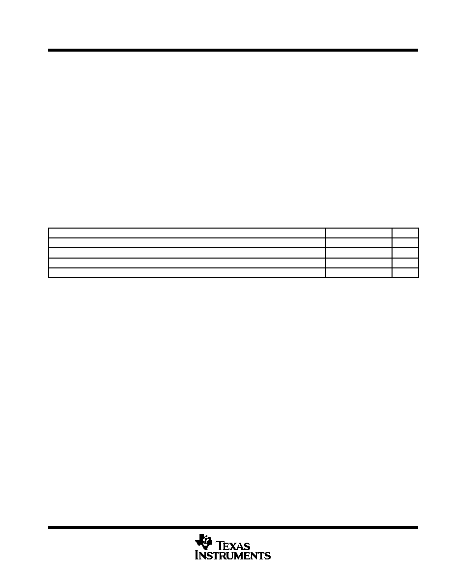
recommended operating conditions
MIN
TYP
MAX
UNIT
Main input voltage, VI (see Notes 1 and 2)
3
5.25
V
Enable input voltage, V(EN) (see Notes 1 and 2)
0
VI
V
Power okay voltage, V(POK) (see Notes 1 and 2)
0
VI
V
Operating ambient temperature, TA
0
70
░
C
NOTES:
1. All voltage values are with respect to GND.
2. Absolute negative voltage on these terminals should not go below ¡0.5 V.
TPPM0125
150-mA LOW DROPOUT REGULATOR WITH POK
SLVS388 ¡ JULY 2001
4
POST OFFICE BOX 655303
À
DALLAS, TEXAS 75265
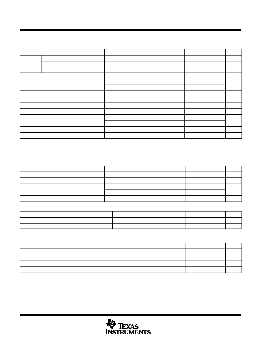
electrical characteristics, T
A
= 25
░
C, V
I
=5 V, V
(EN)
= V
I
, I
O
= 100
Á
A, C
L
= 1
Á
F(unless otherwise noted)
regulator V
O
PARAMETER
TEST CONDITIONS
MIN
TYP
MAX
UNITS
Output voltage
IO = 25 mA
1.2
V
VO
Output voltage accuracy
IO = 0
¡1%
1%
VO
Output voltage accuracy
IO = 50 mA, TA = 0
░
C to 70
░
C (see Note 4)
¡2%
2%
IQ
Quiescent supply current
V(EN)
0.8 V
1
Á
A
I
Ground terminal current (see Note 5)
IO = 0
150
A
I(GND)
Ground terminal current (see Note 5)
IO = 150 mA
150
Á
A
IL
Output load current
150
mA
I(Limit)
Output current limit
VO = 0
160
300
mA
V(LNR)
Line regulation
VI = 3 V to 5.25 V
10
mV
V(LDR)
Load regulation
IO = 0.1 mA to150 mA, See Note 6
2%
3%
V
V
Dropout voltage
IO = 100
Á
A
1
V
VI ¡ VO
Dropout voltage
IO = 150 mA
1
V
CL
Load capacitance
ESR and capacitance tradeoffs
1
Á
F
I(REV)
Reverse output current on VI
VI = GND, VO = regulated voltage
50
Á
A
NOTES:
4. Assured by design, not tested in production.
5. Ground terminal current is the regulator quiescent current drawn from the supply to support the load current.
6. Regulation is measured at constant junction temperature using low duty cycle pulse testing. Devices are tested for load regulation
in the load range from 0.1 mA to 150 mA.
enable input
PARAMETER
TEST CONDITIONS
MIN
TYP
MAX
UNITS
VIL
Regulated shutdown
VI = 3 V to 5.25 V regulated shutdown
0.8
V
VIH
Regulated enabled
VI = 3 V to 5.25 V regulated enabled
2
V
I
Enable input current
Shutdown, VIL
0.8 V
0.01
A
I(EN)
Enable input current
Enabled, VIH
2 V
0.01
Á
A
Resistance discharge
V(EN)
0.8 V
500
thermal protection (see Note 4)
PARAMETER
TEST CONDITIONS
MIN
TYP
MAX
UNITS
T(SD)
Thermal shutdown
165
░
C
T(SDHYS)
Hysteresis
15
░
C
NOTE 4: Assured by design, not tested in production.
power okay (see Note 7)
PARAMETER
TEST CONDITIONS
MIN
TYP
MAX
UNITS
V(POKLO)
Low threshold
Output falls % of VO (power NOT okay)
85%
V(POKTH)
High threshold
Output reaches % of VO, starts delay timer (power okay)
90%
VOL
VO out of regulation
Fault condition, IOL = 100
Á
A
0.4
V
Ilkg
Leakage current
VI = 5 V
1
Á
A
NOTE 7: Power okay is a function of the output voltage being 5% lower than the specified range. The function is a detection of one of the following:
over current, over temperature, or dropout.
TPPM0125
150-mA LOW DROPOUT REGULATOR WITH POK
SLVS388 ¡ JULY 2001
5
POST OFFICE BOX 655303
À
DALLAS, TEXAS 75265
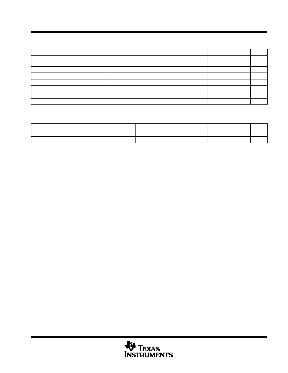
switching characteristics (see Note 4),T
A
= 25
░
C, V
I
= 5 V, V
(EN)
= V
I
, I
O
= 100
Á
A, C
L
= 1
Á
F(unless
otherwise noted)
PARAMETER
TEST CONDITIONS
MIN
TYP
MAX
UNIT
Power up overshoot
Maximum voltage overshoot allowed on output during
powerup
1%
t(STEP)
Output transient time limit
Time for output to return within specified regulation range
5
Á
s
Output transient voltage limit
Voltage that load step can affect the nominal output voltage
1%
I(SR)
Load step current slew rate
IL = 0.1 mA to 150 mA
10
mA/
Á
s
tr
Power up rise time
50
Á
s
tf
Power down fall time
Discharge resistance = 500
, VO < 1.08 V
60
Á
s
td(POK)
Power okay delay time
VI > V(POKTH) until POK
2.5
ms
NOTE 4: Assured by design, not tested in production.
thermal resistance
PARAMETER
TEST CONDITIONS
MIN
TYP
MAX
UNIT
R
JC
Thermal impedance, junction-to-case
145
░
C/W
R
JA
Thermal impedance, junction-to-ambient
235
░
C/W