
TPIC5223L
2-CHANNEL INDEPENDENT GATE-PROTECTED LOGIC-LEVEL
POWER DMOS ARRAY
SLIS043A NOVEMBER 1994 REVISED SEPTEMBER 1995
1
POST OFFICE BOX 655303
·
DALLAS, TEXAS 75265
D
Low r
DS(on)
. . . 0.38
Typ
D
Voltage Output . . . 60 V
D
Input Protection Circuitry . . . 18 V
D
Pulsed Current . . . 3 A Per Channel
D
Extended ESD Capability . . . 4000 V
D
Direct Logic-Level Interface
description
The TPIC5223L is a monolithic gate-protected logic-level power DMOS array that consists of two electrically
isolated independent N-channel enhancement-mode DMOS transistors. Each transistor features integrated
high-current zener diodes (Z
CXa
and Z
CXb
) to prevent gate damage in the event that an overstress condition
occurs. These zener diodes also provide up to 4000 V of ESD protection when tested using the human-body
model of a 100-pF capacitor in series with a 1.5-k
resistor.
The TPIC5223L is offered in a standard eight-pin small-outline surface-mount (D) package and is characterized
for operation over the case temperature of 40
°
C to 125
°
C.
schematic
D1
Z1
DRAIN1
GATE1
SOURCE1
Q1
7
8
D2
Z2
DRAIN2
GATE2
SOURCE2
Q2
3
4
2
GND
1
6
ZC1b
ZC1a
ZC2b
ZC2a
NOTE A: For correct operation, no terminal may be taken below GND.
Copyright
©
1995, Texas Instruments Incorporated
PRODUCTION DATA information is current as of publication date.
Products conform to specifications per the terms of Texas Instruments
standard warranty. Production processing does not necessarily include
testing of all parameters.
1
2
3
4
8
7
6
5
GND
SOURCE1
GATE2
DRAIN2
DRAIN1
GATE1
SOURCE2
NC
D PACKAGE
(TOP VIEW)
NC No internal connection

TPIC5223L
2-CHANNEL INDEPENDENT GATE-PROTECTED LOGIC-LEVEL
POWER DMOS ARRAY
SLIS043A NOVEMBER 1994 REVISED SEPTEMBER 1995
2
POST OFFICE BOX 655303
·
DALLAS, TEXAS 75265
absolute maximum ratings over operating case temperature range (unless otherwise noted)
Drain-to-source voltage, V
DS
60 V
. . . . . . . . . . . . . . . . . . . . . . . . . . . . . . . . . . . . . . . . . . . . . . . . . . . . . . . . . . . . . .
Source-to-GND voltage
100 V
. . . . . . . . . . . . . . . . . . . . . . . . . . . . . . . . . . . . . . . . . . . . . . . . . . . . . . . . . . . . . . . . . . . .
Drain-to-GND voltage
100 V
. . . . . . . . . . . . . . . . . . . . . . . . . . . . . . . . . . . . . . . . . . . . . . . . . . . . . . . . . . . . . . . . . . . . .
Gate-to-source voltage range, V
GS
9 V to 18 V
. . . . . . . . . . . . . . . . . . . . . . . . . . . . . . . . . . . . . . . . . . . . . . . . . . .
Continuous drain current, each output, T
C
= 25
°
C 1
A
. . . . . . . . . . . . . . . . . . . . . . . . . . . . . . . . . . . . . . . . . . . . . . .
Continuous source-to-drain diode current, T
C
= 25
°
C 1
A
. . . . . . . . . . . . . . . . . . . . . . . . . . . . . . . . . . . . . . . . . . . .
Pulsed drain current, each output, I
max
, T
C
= 25
°
C (see Note 1 and Figure 15)
3 A
. . . . . . . . . . . . . . . . . . . . .
Continuous gate-to-source zener diode current, T
C
= 25
°
C
±
50 mA
. . . . . . . . . . . . . . . . . . . . . . . . . . . . . . . . . .
Pulsed gate-to-source zener-diode current, T
C
= 25
°
C
±
500 mA
. . . . . . . . . . . . . . . . . . . . . . . . . . . . . . . . . . . . .
Single-pulse avalanche energy, E
AS
, T
C
= 25
°
C (see Figures 4 and 16)
108 mJ
. . . . . . . . . . . . . . . . . . . . . . .
Continuous total power dissipation, T
C
= 25
°
C (see Figure 15)
0.95 W
. . . . . . . . . . . . . . . . . . . . . . . . . . . . . . . . .
Operating virtual junction temperature range, T
J
40
°
C to 150
°
C
. . . . . . . . . . . . . . . . . . . . . . . . . . . . . . . . . . . .
Operating case temperature range, T
C
40
°
C to 125
°
C
. . . . . . . . . . . . . . . . . . . . . . . . . . . . . . . . . . . . . . . . . . . .
Storage temperature range, T
stg
65
°
C to 150
°
C
. . . . . . . . . . . . . . . . . . . . . . . . . . . . . . . . . . . . . . . . . . . . . . . . . .
Lead temperature 1,6 mm (1/16 inch) from case for 10 seconds
260
°
C
. . . . . . . . . . . . . . . . . . . . . . . . . . . . . . .
Stresses beyond those listed under "absolute maximum ratings" may cause permanent damage to the device. These are stress ratings only, and
functional operation of the device at these or any other conditions beyond those indicated under "recommended operating conditions" is not
implied. Exposure to absolute-maximum-rated conditions for extended periods may affect device reliability.
NOTE 1: Pulse duration = 10 ms, duty cycle = 2%
TPIC5223L
2-CHANNEL INDEPENDENT GATE-PROTECTED LOGIC-LEVEL
POWER DMOS ARRAY
SLIS043A NOVEMBER 1994 REVISED SEPTEMBER 1995
3
POST OFFICE BOX 655303
·
DALLAS, TEXAS 75265
electrical characteristics, T
C
= 25
°
C (unless otherwise noted)
PARAMETER
TEST CONDITIONS
MIN
TYP
MAX
UNIT
V(BR)DSX Drain-to-source breakdown voltage
ID = 250
µ
A,
VGS = 0
60
V
VGS(th)
Gate-to-source threshold voltage
ID = 1 mA,
See Figure 5
VDS = VGS,
1.5
2.05
2.2
V
V(BR)GS
Gate-to-source breakdown voltage
IGS = 250
µ
A
18
V
V(BR)SG
Source-to-gate breakdown voltage
ISG = 250
µ
A
9
V
V(BR)
Reverse drain-to-GND breakdown voltage
(across D1, D2)
Drain-to-GND current = 250
µ
A
100
V
VDS(on)
Drain-to-source on-state voltage
ID = 1 A,
See Notes 2 and 3
VGS = 5 V,
0.375
0.425
V
VF(SD)
Forward on-state voltage, source-to-drain
IS = 1 A,
VGS = 0 (Z1, Z2),
See Notes 2 and 3 and Figure 12
0.85
1.2
V
VF
Forward on-state voltage, GND-to-drain
ID = 1 A (D1, D2),
See Notes 2 and 3
3
V
IDSS
Zero gate voltage drain current
VDS = 48 V,
TC = 25
°
C
0.05
1
µ
A
IDSS
Zero-gate-voltage drain current
DS
,
VGS = 0
TC = 125
°
C
0.5
10
µ
A
IGSSF
Forward-gate current, drain short circuited to source
VGS = 15 V,
VDS = 0
20
200
nA
IGSSR
Reverse-gate current, drain short circuited to source
VSG = 5 V,
VDS = 0
10
100
nA
Ilk
Leakage current drain to GND
VDGND = 48 V
TC = 25
°
C
0.05
1
µ
A
Ilkg
Leakage current, drain-to-GND
VDGND = 48 V
TC = 125
°
C
0.5
10
µ
A
rDS( )
Static drain to source on state resistance
VGS = 5 V,
ID = 1 A,
TC = 25
°
C
0.38
0.43
rDS(on)
Static drain-to-source on-state resistance
D
,
See Notes 2 and 3
and Figures 6 and 7
TC = 125
°
C
0.61
0.65
gfs
Forward transconductance
VDS = 15 V,
ID = 500 mA,
See Notes 2 and 3 and Figure 9
1.2
1.49
S
Ciss
Short-circuit input capacitance, common source
150
190
Coss
Short-circuit output capacitance, common source
VDS = 25 V,
VGS = 0,
100
125
pF
Crss
Short-circuit reverse transfer capacitance,
common source
f = 1 MHz,
See Figure 11
40
50
F
NOTES:
2. Technique should limit TJ TC to 10
°
C maximum.
3. These parameters are measured with voltage-sensing contacts separate from the current-carrying contacts.
source-to-drain and GND-to-drain diode characteristics, T
C
= 25
°
C
PARAMETER
TEST CONDITIONS
MIN
TYP
MAX
UNIT
t
Reverse recovery time
Z1 and Z2
50
ns
trr
Reverse-recovery time
IS = 500 mA,
VGS = 0
VDS = 48 V,
di/dt = 100 A/
µ
s
D1 and D2
210
ns
QRR
Total diode charge
VGS = 0,
See Figures 1 and 14
di/dt = 100 A/
µ
s,
Z1 and Z2
50
nC
QRR
Total diode charge
See Figures 1 and 14
D1 and D2
800
nC
TPIC5223L
2-CHANNEL INDEPENDENT GATE-PROTECTED LOGIC-LEVEL
POWER DMOS ARRAY
SLIS043A NOVEMBER 1994 REVISED SEPTEMBER 1995
4
POST OFFICE BOX 655303
·
DALLAS, TEXAS 75265
resistive-load switching characteristics, T
C
= 25
°
C
PARAMETER
TEST CONDITIONS
MIN
TYP
MAX
UNIT
td(on)
Turn-on delay time
34
70
td(off)
Turn-off delay time
VDD = 25 V,
RL = 50
,
tr1 = 10 ns,
20
40
ns
tr1
Rise time
DD
,
tf1 = 10 ns,
L
,
See Figure 2
r1
,
28
55
ns
tf2
Fall time
15
30
Qg
Total gate charge
V
48 V
I
500
A
V
5 V
3.1
3.8
Qgs(th) Threshold gate-to-source charge
VDS = 48 V,
See Figure 3
ID = 500 mA, VGS = 5 V,
0.5
0.6
nC
Qgd
Gate-to-drain charge
See Figure 3
1.9
2.3
LD
Internal drain inductance
5
nH
LS
Internal source inductance
5
nH
Rg
Internal gate resistance
0.25
thermal resistance
PARAMETER
TEST CONDITIONS
MIN
TYP
MAX
UNIT
R
JA
Junction-to-ambient thermal resistance
See Notes 4 and 7
130
R
JB
Junction-to-board thermal resistance
See Notes 5 and 7
78.6
°
C/W
R
JP
Junction-to-pin thermal resistance
See Notes 6 and 7
34
NOTES:
4. Package mounted on an FR4 printed-circuit board with no heatsink.
5. Package mounted on a 24 in2, 4-layer FR4 printed-circuit board.
6. Package mounted in intimate contact with infinite heatsink.
7. All outputs with equal power
PARAMETER MEASUREMENT INFORMATION
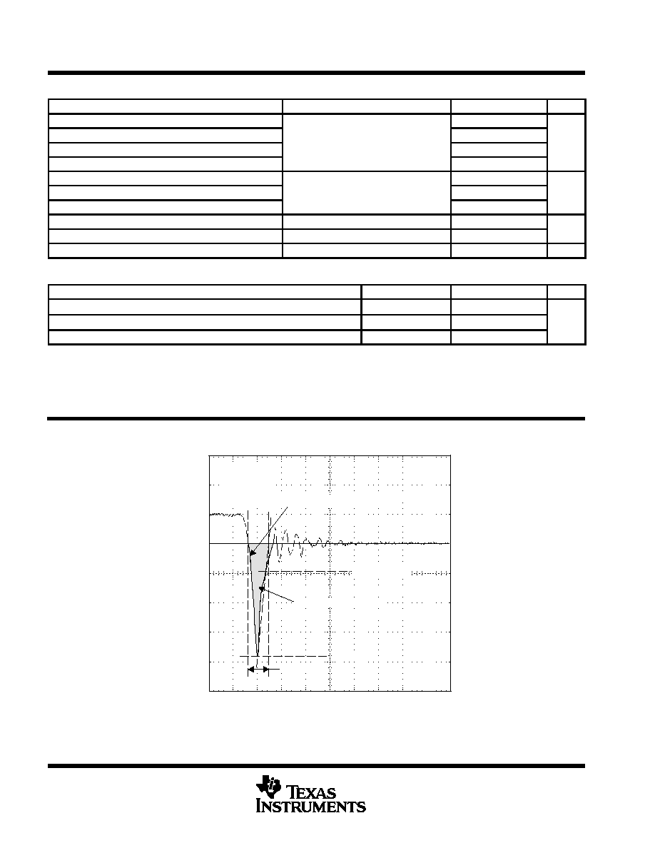
Time ns
0
50
100
150
200
250
300
350
400
450
500
IRM = maximum recovery current
0
0.5
1
1.5
2
2.5
1.5
1
0.5
Source-to-Drain Diode Current
A
I S
IRM
VDS = 48 V
VGS = 0
TJ = 25
°
C
Z1, and Z2
Reverse di/dt = 100 A/
µ
s
25% of IRM
trr(SD)
Shaded Area = QRR
The above waveform is representative of D1 and D2 in shape only.
Figure 1. Reverse-Recovery-Current Waveform of Source-to-Drain Diode
TPIC5223L
2-CHANNEL INDEPENDENT GATE-PROTECTED LOGIC-LEVEL
POWER DMOS ARRAY
SLIS043A NOVEMBER 1994 REVISED SEPTEMBER 1995
5
POST OFFICE BOX 655303
·
DALLAS, TEXAS 75265
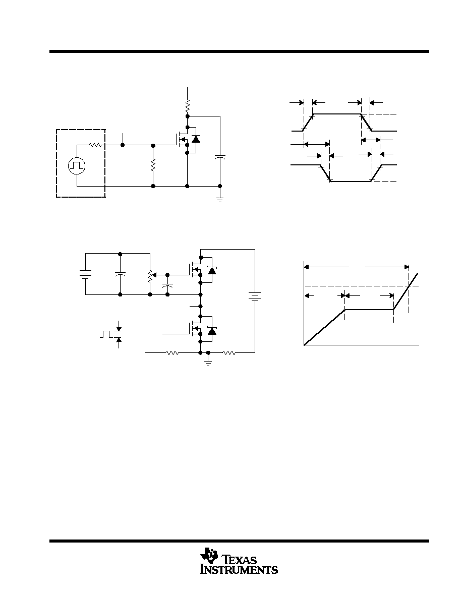
PARAMETER MEASUREMENT INFORMATION
Pulse Generator
50
Rgen
50
VGS
VDD = 25 V
DUT
VDS
TEST CIRCUIT
VDD
VDS(on)
tf2
td(on)
tr2
td(off)
VOLTAGE WAVEFORMS
VGS
VDS
RL
CL = 30 pF
(see Note A)
tf1
tr1
5 V
0 V
NOTE A: CL includes probe and jig capacitance.
Figure 2. Resistive-Switching Test Circuit and Voltage Waveforms
5 V
VOLTAGE WAVEFORM
Qgd
Time
Gate Voltage
VGS
12-V
Battery
0.2
µ
F
50 k
0.3
µ
F
Current
Regulator
DUT
Same Type
as DUT
0 V
IG = 100
µ
A
IG Current-
Sampling Resistor
ID Current-
Sampling Resistor
VDD
TEST CIRCUIT
Qgs(th)
VDS
Qg
Figure 3. Gate-Charge Test Circuit and Voltage Waveform