TPA4861
1-W AUDIO POWER AMPLIFIER
SLOS163B ş SEPTEMBER 1996 ş REVISED MARCH 2000
1
POST OFFICE BOX 655303
Ě
DALLAS, TEXAS 75265
D
1-W BTL Output (5 V, 0.11 % THD+N)
D
3.3-V and 5-V Operation
D
No Output Coupling Capacitors Required
D
Shutdown Control (I
DD
= 0.6
Á
A)
D
Uncompensated Gains of 2 to 20 (BTL
Mode)
D
Surface-Mount Packaging
D
Thermal and Short-Circuit Protection
D
High Supply Ripple Rejection Ratio
(56 dB at 1 kHz)
D
LM4861 Drop-In Compatible
description
The TPA4861 is a bridge-tied load (BTL) audio power amplifier capable of delivering 1 W of continuous average
power into an 8-
load at 0.2% THD+N from a 5-V power supply in voiceband frequencies (f < 5 kHz). A BTL
configuration eliminates the need for external coupling capacitors on the output in most applications. Gain is
externally configured by means of two resistors and does not require compensation for settings of 2 to 20.
Features of the amplifier are a shutdown function for power-sensitive applications as well as internal thermal
and short-circuit protection. The TPA4861 works seamlessly with TI's TPA4860 in stereo applications. The
amplifier is available in an 8-pin SOIC surface-mount package that reduces board space and facilitates
automated assembly.
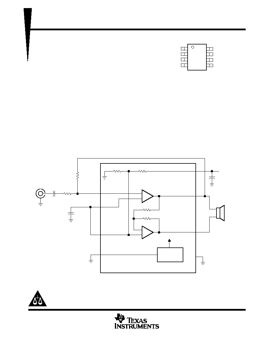
Audio
Input
Bias
Control
VDD
1 W
6
5
8
7
VO1
VO2
VDD
1
2
3
4
IN +
IN ş
BYPASS
SHUTDOWN
VDD/2
CI
RI
RF
CS
CB
ş
+
ş
+
GND
Please be aware that an important notice concerning availability, standard warranty, and use in critical applications of
Texas Instruments semiconductor products and disclaimers thereto appears at the end of this data sheet.
Copyright
ę
2000, Texas Instruments Incorporated
PRODUCTION DATA information is current as of publication date.
Products conform to specifications per the terms of Texas Instruments
standard warranty. Production processing does not necessarily include
testing of all parameters.
1
2
3
4
8
7
6
5
SHUTDOWN
BYPASS
IN+
INş
V
O
2
GND
V
DD
V
O
1
D PACKAGE
(TOP VIEW)

TPA4861
1-W AUDIO POWER AMPLIFIER
SLOS163B ş SEPTEMBER 1996 ş REVISED MARCH 2000
2
POST OFFICE BOX 655303
Ě
DALLAS, TEXAS 75265
AVAILABLE OPTIONS
PACKAGED DEVICE
TA
SMALL OUTLINE
(D)
ş 40
░
C to 85
░
C
TPA4861D
The D package is available tape and reeled. To order a tape and
reeled part, add the suffix R to the part number (e.g., TPA4861DR).
Terminal Functions
TERMINAL
I/O
DESCRIPTION
NAME
NO.
I/O
DESCRIPTION
BYPASS
2
I
BYPASS is the tap to the voltage divider for internal mid-supply bias. This terminal should be connected
to a 0.1
Á
F ş 1.0
Á
F capacitor when used as an audio power amplifier.
GND
7
GND is the ground connection.
INş
4
I
INş is the inverting input. INş is typically used as the audio input terminal.
IN+
3
I
IN+ is the noninverting input. IN+ is typically tied to the BYPASS terminal.
SHUTDOWN
1
I
SHUTDOWN places the entire device in shutdown mode when held high (IDD
0.6
Á
A).
VO1
5
O
VO1 is the positive BTL output.
VO2
8
O
VO2 is the negative BTL output.
VDD
6
VDD is the supply voltage terminal.
absolute maximum ratings over operating free-air temperature range (unless otherwise noted)
Supply voltage, V
DD
6 V
. . . . . . . . . . . . . . . . . . . . . . . . . . . . . . . . . . . . . . . . . . . . . . . . . . . . . . . . . . . . . . . . . . . . . . . .
Input voltage, V
I
ş0.3 V to V
DD
+0.3 V
. . . . . . . . . . . . . . . . . . . . . . . . . . . . . . . . . . . . . . . . . . . . . . . . . . . . . . . . . . . .
Continuous total power dissipation
Internally Limited (see Dissipation Rating Table)
. . . . . . . . . . . . . . . . . . . . .
Operating free-air temperature range, T
A
ş 40
░
C to 85
░
C
. . . . . . . . . . . . . . . . . . . . . . . . . . . . . . . . . . . . . . . . . . . .
Operating junction temperature range, T
J
ş 40
░
C to 150
░
C
. . . . . . . . . . . . . . . . . . . . . . . . . . . . . . . . . . . . . . . . . . .
Storage temperature range, T
stg
ş65
░
C to 150
░
C
. . . . . . . . . . . . . . . . . . . . . . . . . . . . . . . . . . . . . . . . . . . . . . . . . . .
Lead temperature 1,6 mm (1/16 inch) from case for 10 seconds
260
░
C
. . . . . . . . . . . . . . . . . . . . . . . . . . . . . . .
Stresses beyond those listed under "absolute maximum ratings" may cause permanent damage to the device. These are stress ratings only, and
functional operation of the device at these or any other conditions beyond those indicated under "recommended operating conditions" is not
implied. Exposure to absolute-maximum-rated conditions for extended periods may affect device reliability.
DISSIPATION RATING TABLE
PACKAGE
TA
25
░
C
DERATING FACTOR
TA = 70
░
C
TA = 85
░
C
D
725 mW
5.8 mW/
░
C
464 mW
377 mW
recommended operating conditions
MIN
MAX
UNIT
┴┴┴┴┴┴┴┴┴┴┴┴┴┴┴┴┴┴┴┴┴┴┴┴┴┴┴┴
┴┴┴┴┴┴┴┴┴┴┴┴┴┴┴┴┴┴┴┴┴┴┴┴┴┴┴┴
Supply voltage, VDD
┴┴┴
┴┴┴
2.7
┴┴┴
┴┴┴
5.5
┴┴┴
┴┴┴
V
┴┴┴┴┴┴┴┴┴┴┴┴┴┴┴
┴┴┴┴┴┴┴┴┴┴┴┴┴┴┴
Common mode input voltage VIC
┴┴┴┴┴┴┴┴┴┴┴┴┴┴
┴┴┴┴┴┴┴┴┴┴┴┴┴┴
VDD = 3 V
┴┴┴
┴┴┴
1.25
┴┴┴
┴┴┴
2.7
┴┴┴
┴┴┴
V
┴┴┴┴┴┴┴┴┴┴┴┴┴┴┴
┴┴┴┴┴┴┴┴┴┴┴┴┴┴┴
Common-mode input voltage, VIC
┴┴┴┴┴┴┴┴┴┴┴┴┴┴
┴┴┴┴┴┴┴┴┴┴┴┴┴┴
VDD = 5 V
┴┴┴
┴┴┴
1.25
┴┴┴
┴┴┴
4.5
┴┴┴
┴┴┴
V
┴┴┴┴┴┴┴┴┴┴┴┴┴┴┴┴┴┴┴┴┴┴┴┴┴┴┴┴
┴┴┴┴┴┴┴┴┴┴┴┴┴┴┴┴┴┴┴┴┴┴┴┴┴┴┴┴
Operating free-air temperature, TA
┴┴┴
┴┴┴
ş 40
┴┴┴
┴┴┴
85
┴┴┴
┴┴┴
░
C

TPA4861
1-W AUDIO POWER AMPLIFIER
SLOS163B ş SEPTEMBER 1996 ş REVISED MARCH 2000
3
POST OFFICE BOX 655303
Ě
DALLAS, TEXAS 75265
electrical characteristics at specified free-air temperature, V
DD
= 3.3 V (unless otherwise noted)
PARAMETER
TEST CONDITIONS
TPA4861
UNIT
PARAMETER
TEST CONDITIONS
MIN
TYP
MAX
UNIT
┴┴┴
┴┴┴
VOO
┴┴┴┴┴┴┴┴┴┴┴┴┴┴┴┴┴┴
┴┴┴┴┴┴┴┴┴┴┴┴┴┴┴┴┴┴
Output offset voltage
┴┴┴┴┴┴
┴┴┴┴┴┴
See Note 1
┴┴┴
┴┴┴
┴┴┴
┴┴┴
┴┴┴
┴┴┴
20
┴┴┴
┴┴┴
mV
┴┴┴
┴┴┴
PSRR
┴┴┴┴┴┴┴┴┴┴┴┴┴┴┴┴┴┴
┴┴┴┴┴┴┴┴┴┴┴┴┴┴┴┴┴┴
Power supply rejection ratio (
VDD /
VOO)
┴┴┴┴┴┴
┴┴┴┴┴┴
VDD = 3.2 V to 3.4 V
┴┴┴
┴┴┴
┴┴┴
┴┴┴
75
┴┴┴
┴┴┴
┴┴┴
┴┴┴
dB
┴┴┴
┴┴┴
IDD
┴┴┴┴┴┴┴┴┴┴┴┴┴┴┴┴┴┴
┴┴┴┴┴┴┴┴┴┴┴┴┴┴┴┴┴┴
Supply current
┴┴┴┴┴┴
┴┴┴┴┴┴
┴┴┴
┴┴┴
┴┴┴
┴┴┴
2.5
┴┴┴
┴┴┴
┴┴┴
┴┴┴
mA
┴┴┴
┴┴┴
IDD(SD)
┴┴┴┴┴┴┴┴┴┴┴┴┴┴┴┴┴┴
┴┴┴┴┴┴┴┴┴┴┴┴┴┴┴┴┴┴
Supply current, shutdown
┴┴┴┴┴┴
┴┴┴┴┴┴
┴┴┴
┴┴┴
┴┴┴
┴┴┴
0.6
┴┴┴
┴┴┴
┴┴┴
┴┴┴
Á
A
NOTE 1: At 3 V < VDD < 5 V the dc output voltage is approximately VDD/2.
operating characteristics, V
DD
= 3.3 V, T
A
= 25
░
C, R
L
= 8
PARAMETER
TEST CONDITIONS
TPA4861
UNIT
PARAMETER
TEST CONDITIONS
MIN
TYP
MAX
UNIT
┴┴┴
┴┴┴
PO
┴┴┴┴┴┴┴┴┴┴┴┴┴
┴┴┴┴┴┴┴┴┴┴┴┴┴
Output power see Note 2
┴┴┴┴┴┴┴┴
┴┴┴┴┴┴┴┴
THD = 0.2%, f = 1 kHz,
┴┴┴┴
┴┴┴┴
AV = ş2 V/V
┴┴┴
┴┴┴
┴┴┴
┴┴┴
400
┴┴┴
┴┴┴
┴┴┴
┴┴┴
mW
┴┴┴
┴┴┴
PO
┴┴┴┴┴┴┴┴┴┴┴┴┴
┴┴┴┴┴┴┴┴┴┴┴┴┴
Output power, see Note 2
┴┴┴┴┴┴┴┴
┴┴┴┴┴┴┴┴
THD = 2%, f = 1 kHz,
┴┴┴┴
┴┴┴┴
AV = ş2 V/V
┴┴┴
┴┴┴
┴┴┴
┴┴┴
500
┴┴┴
┴┴┴
┴┴┴
┴┴┴
mW
┴┴┴
┴┴┴
BOM
┴┴┴┴┴┴┴┴┴┴┴┴┴
┴┴┴┴┴┴┴┴┴┴┴┴┴
Maximum output power bandwidth
┴┴┴┴┴┴┴┴
┴┴┴┴┴┴┴┴
Gain = ş10 V/V,
┴┴┴┴
┴┴┴┴
THD = 2%
┴┴┴
┴┴┴
┴┴┴
┴┴┴
20
┴┴┴
┴┴┴
┴┴┴
┴┴┴
kHz
┴┴┴
┴┴┴
B1
┴┴┴┴┴┴┴┴┴┴┴┴┴
┴┴┴┴┴┴┴┴┴┴┴┴┴
Unity-gain bandwidth
┴┴┴┴┴┴┴┴┴┴┴
┴┴┴┴┴┴┴┴┴┴┴
Open Loop
┴┴┴
┴┴┴
┴┴┴
┴┴┴
1.5
┴┴┴
┴┴┴
┴┴┴
┴┴┴
MHz
┴┴┴
┴┴┴
┴┴┴┴┴┴┴┴┴
┴┴┴┴┴┴┴┴┴
Supply ripple rejection ratio
┴┴┴┴┴
┴┴┴┴┴
BTL
┴┴┴┴┴┴┴┴
┴┴┴┴┴┴┴┴
f = 1 kHz,
┴┴┴┴
┴┴┴┴
CB = 0.1
Á
F
┴┴┴
┴┴┴
┴┴┴
┴┴┴
56
┴┴┴
┴┴┴
┴┴┴
┴┴┴
dB
┴┴┴
┴┴┴
┴┴┴┴┴┴┴┴┴
┴┴┴┴┴┴┴┴┴
Supply ripple rejection ratio
┴┴┴┴┴
┴┴┴┴┴
SE
┴┴┴┴┴┴┴┴
┴┴┴┴┴┴┴┴
f = 1 kHz,
┴┴┴┴
┴┴┴┴
CB = 0.1
Á
F
┴┴┴
┴┴┴
┴┴┴
┴┴┴
30
┴┴┴
┴┴┴
┴┴┴
┴┴┴
dB
┴┴┴
┴┴┴
Vn
┴┴┴┴┴┴┴┴┴┴┴┴┴
┴┴┴┴┴┴┴┴┴┴┴┴┴
Noise output voltage, see Note 3
┴┴┴┴┴┴┴┴┴┴┴
┴┴┴┴┴┴┴┴┴┴┴
Gain = ş2 V/V
┴┴┴
┴┴┴
┴┴┴
┴┴┴
20
┴┴┴
┴┴┴
┴┴┴
┴┴┴
Á
V
NOTES:
2. Output power is measured at the output terminals of the device.
3. Noise voltage is measured in a bandwidth of 20 Hz to 20 kHz.
electrical characteristics at specified free-air temperature range, V
DD
= 5 V (unless otherwise
noted)
PARAMETER
TEST CONDITION
TPA4861
UNIT
PARAMETER
TEST CONDITION
MIN
TYP
MAX
UNIT
┴┴┴
┴┴┴
VOO
┴┴┴┴┴┴┴┴┴┴┴┴┴┴┴┴┴┴
┴┴┴┴┴┴┴┴┴┴┴┴┴┴┴┴┴┴
Output offset voltage
┴┴┴┴┴┴
┴┴┴┴┴┴
See Note 1
┴┴┴
┴┴┴
┴┴┴
┴┴┴
┴┴┴
┴┴┴
20
┴┴┴
┴┴┴
mV
┴┴┴
┴┴┴
PSRR
┴┴┴┴┴┴┴┴┴┴┴┴┴┴┴┴┴┴
┴┴┴┴┴┴┴┴┴┴┴┴┴┴┴┴┴┴
Power supply rejection ratio (
VDD /
VOO)
┴┴┴┴┴┴
┴┴┴┴┴┴
VDD = 4.9 V to 5.1 V
┴┴┴
┴┴┴
┴┴┴
┴┴┴
70
┴┴┴
┴┴┴
┴┴┴
┴┴┴
dB
┴┴┴
┴┴┴
IDD
┴┴┴┴┴┴┴┴┴┴┴┴┴┴┴┴┴┴
┴┴┴┴┴┴┴┴┴┴┴┴┴┴┴┴┴┴
Supply current
┴┴┴┴┴┴
┴┴┴┴┴┴
┴┴┴
┴┴┴
┴┴┴
┴┴┴
3.5
┴┴┴
┴┴┴
┴┴┴
┴┴┴
mA
┴┴┴
┴┴┴
IDD(SD)
┴┴┴┴┴┴┴┴┴┴┴┴┴┴┴┴┴┴
┴┴┴┴┴┴┴┴┴┴┴┴┴┴┴┴┴┴
Supply current, shutdown
┴┴┴┴┴┴
┴┴┴┴┴┴
┴┴┴
┴┴┴
┴┴┴
┴┴┴
0.6
┴┴┴
┴┴┴
┴┴┴
┴┴┴
Á
A
NOTE 1: At 3 V < VDD < 5 V the dc output voltage is approximately VDD/2.
operating characteristic, V
DD
= 5 V, T
A
= 25
░
C, R
L
= 8
PARAMETER
TEST CONDITIONS
TPA4861
UNIT
PARAMETER
TEST CONDITIONS
MIN
TYP
MAX
UNIT
┴┴┴
┴┴┴
PO
┴┴┴┴┴┴┴┴┴┴┴┴┴
┴┴┴┴┴┴┴┴┴┴┴┴┴
Output power see Note 2
┴┴┴┴┴┴┴┴
┴┴┴┴┴┴┴┴
THD = 0.2%, f = 1 kHz,
┴┴┴┴
┴┴┴┴
AV = ş2 V/V
┴┴┴
┴┴┴
┴┴┴
┴┴┴
1000
┴┴┴
┴┴┴
┴┴┴
┴┴┴
mW
┴┴┴
┴┴┴
PO
┴┴┴┴┴┴┴┴┴┴┴┴┴
┴┴┴┴┴┴┴┴┴┴┴┴┴
Output power, see Note 2
┴┴┴┴┴┴┴┴
┴┴┴┴┴┴┴┴
THD = 2%, f = 1 kHz,
┴┴┴┴
┴┴┴┴
AV = ş2 V/V
┴┴┴
┴┴┴
┴┴┴
┴┴┴
1100
┴┴┴
┴┴┴
┴┴┴
┴┴┴
mW
┴┴┴
┴┴┴
BOM
┴┴┴┴┴┴┴┴┴┴┴┴┴
┴┴┴┴┴┴┴┴┴┴┴┴┴
Maximum output power bandwidth
┴┴┴┴┴┴┴┴
┴┴┴┴┴┴┴┴
Gain = ş10 V/V,
┴┴┴┴
┴┴┴┴
THD = 2%
┴┴┴
┴┴┴
┴┴┴
┴┴┴
20
┴┴┴
┴┴┴
┴┴┴
┴┴┴
kHz
┴┴┴
┴┴┴
B1
┴┴┴┴┴┴┴┴┴┴┴┴┴
┴┴┴┴┴┴┴┴┴┴┴┴┴
Unity-gain bandwidth
┴┴┴┴┴┴┴┴┴┴┴
┴┴┴┴┴┴┴┴┴┴┴
Open Loop
┴┴┴
┴┴┴
┴┴┴
┴┴┴
1.5
┴┴┴
┴┴┴
┴┴┴
┴┴┴
MHz
┴┴┴
┴┴┴
┴┴┴┴┴┴┴┴┴
┴┴┴┴┴┴┴┴┴
Supply ripple rejection ratio
┴┴┴┴┴
┴┴┴┴┴
BTL
┴┴┴┴┴┴┴┴
┴┴┴┴┴┴┴┴
f = 1 kHz,
┴┴┴┴
┴┴┴┴
CB = 0.1
Á
F
┴┴┴
┴┴┴
┴┴┴
┴┴┴
56
┴┴┴
┴┴┴
┴┴┴
┴┴┴
dB
┴┴┴
┴┴┴
┴┴┴┴┴┴┴┴┴
┴┴┴┴┴┴┴┴┴
Supply ripple rejection ratio
┴┴┴┴┴
┴┴┴┴┴
SE
┴┴┴┴┴┴┴┴
┴┴┴┴┴┴┴┴
f = 1 kHz,
┴┴┴┴
┴┴┴┴
CB = 0.1
Á
F
┴┴┴
┴┴┴
┴┴┴
┴┴┴
30
┴┴┴
┴┴┴
┴┴┴
┴┴┴
dB
┴┴┴
┴┴┴
Vn
┴┴┴┴┴┴┴┴┴┴┴┴┴
┴┴┴┴┴┴┴┴┴┴┴┴┴
Noise output voltage, see Note 3
┴┴┴┴┴┴┴┴┴┴┴
┴┴┴┴┴┴┴┴┴┴┴
Gain = ş2 V/V
┴┴┴
┴┴┴
┴┴┴
┴┴┴
20
┴┴┴
┴┴┴
┴┴┴
┴┴┴
Á
V
NOTES:
2. Output power is measured at the output terminals of the device.
3. Noise voltage is measured in a bandwidth of 20 Hz to 20 kHz.
TPA4861
1-W AUDIO POWER AMPLIFIER
SLOS163B ş SEPTEMBER 1996 ş REVISED MARCH 2000
4
POST OFFICE BOX 655303
Ě
DALLAS, TEXAS 75265
TYPICAL CHARACTERISTICS
Table of Graphs
┴┴┴┴┴┴┴┴┴┴┴┴┴┴┴┴┴┴┴┴┴┴
┴┴┴┴┴┴┴┴┴┴┴┴┴┴┴┴┴┴┴┴┴┴
┴┴┴┴
┴┴┴┴
FIGURE
┴┴┴┴
┴┴┴┴
VOO
┴┴┴┴┴┴┴┴┴┴┴
┴┴┴┴┴┴┴┴┴┴┴
Output offset voltage
┴┴┴┴┴┴┴┴┴
┴┴┴┴┴┴┴┴┴
Distribution
┴┴┴┴
┴┴┴┴
1,2
┴┴┴┴
┴┴┴┴
IDD
┴┴┴┴┴┴┴┴┴┴┴
┴┴┴┴┴┴┴┴┴┴┴
Supply current distribution
┴┴┴┴┴┴┴┴┴
┴┴┴┴┴┴┴┴┴
vs Free-air temperature
┴┴┴┴
┴┴┴┴
3,4
┴┴┴┴
┴
┴┴
┴
┴┴┴┴
THD+N
┴┴┴┴┴┴┴┴┴┴┴
┴
┴┴┴┴┴┴┴┴┴
┴
┴┴┴┴┴┴┴┴┴┴┴
Total harmonic distortion plus noise
┴┴┴┴┴┴┴┴┴
┴
┴┴┴┴┴┴┴
┴
┴┴┴┴┴┴┴┴┴
vs Frequency
┴┴┴┴
┴
┴┴
┴
┴┴┴┴
5,6,7,8,9,
10,11,15,
16,17,18
┴┴┴┴
┴
┴┴
┴
┴┴┴┴
┴┴┴┴┴┴┴┴┴┴┴
┴
┴┴┴┴┴┴┴┴┴
┴
┴┴┴┴┴┴┴┴┴┴┴
┴┴┴┴┴┴┴┴┴
┴
┴┴┴┴┴┴┴
┴
┴┴┴┴┴┴┴┴┴
vs Output power
┴┴┴┴
┴
┴┴
┴
┴┴┴┴
12,13,14,
19,20,21
┴┴┴┴
┴┴┴┴
IDD
┴┴┴┴┴┴┴┴┴┴┴
┴┴┴┴┴┴┴┴┴┴┴
Supply current
┴┴┴┴┴┴┴┴┴
┴┴┴┴┴┴┴┴┴
vs Supply voltage
┴┴┴┴
┴┴┴┴
22
┴┴┴┴
Vn
┴┴┴┴┴┴┴┴┴┴┴
Output noise voltage
┴┴┴┴┴┴┴┴┴
vs Frequency
┴┴┴┴
23,24
┴┴┴┴
┴┴┴┴
┴┴┴┴┴┴┴┴┴┴┴
┴┴┴┴┴┴┴┴┴┴┴
Maximum package power dissipation
┴┴┴┴┴┴┴┴┴
┴┴┴┴┴┴┴┴┴
vs Free-air temperature
┴┴┴┴
┴┴┴┴
25
┴┴┴┴
┴┴┴┴
┴┴┴┴┴┴┴┴┴┴┴
┴┴┴┴┴┴┴┴┴┴┴
Power dissipation
┴┴┴┴┴┴┴┴┴
┴┴┴┴┴┴┴┴┴
vs Output power
┴┴┴┴
┴┴┴┴
26,27
┴┴┴┴
┴┴┴┴
┴┴┴┴┴┴┴┴┴┴┴
┴┴┴┴┴┴┴┴┴┴┴
Maximum power output
┴┴┴┴┴┴┴┴┴
┴┴┴┴┴┴┴┴┴
vs Free-air temperature
┴┴┴┴
┴┴┴┴
28
┴┴┴┴
┴┴┴┴
┴┴┴┴┴┴┴┴┴┴┴
┴┴┴┴┴┴┴┴┴┴┴
Output power
┴┴┴┴┴┴┴┴┴
┴┴┴┴┴┴┴┴┴
vs Load resistance
┴┴┴┴
┴┴┴┴
29
┴┴┴┴
┴┴┴┴
┴┴┴┴┴┴┴┴┴┴┴
┴┴┴┴┴┴┴┴┴┴┴
Output power
┴┴┴┴┴┴┴┴┴
┴┴┴┴┴┴┴┴┴
vs Supply voltage
┴┴┴┴
┴┴┴┴
30
┴┴┴┴
┴┴┴┴
┴┴┴┴┴┴┴┴┴┴┴
┴┴┴┴┴┴┴┴┴┴┴
Open-loop gain
┴┴┴┴┴┴┴┴┴
┴┴┴┴┴┴┴┴┴
vs Frequency
┴┴┴┴
┴┴┴┴
31
┴┴┴┴
┴┴┴┴
kSVR
┴┴┴┴┴┴┴┴┴┴┴
┴┴┴┴┴┴┴┴┴┴┴
Supply ripple rejection ratio
┴┴┴┴┴┴┴┴┴
┴┴┴┴┴┴┴┴┴
vs Frequency
┴┴┴┴
┴┴┴┴
32,33
TPA4861
1-W AUDIO POWER AMPLIFIER
SLOS163B ş SEPTEMBER 1996 ş REVISED MARCH 2000
5
POST OFFICE BOX 655303
Ě
DALLAS, TEXAS 75265
TYPICAL CHARACTERISTICS
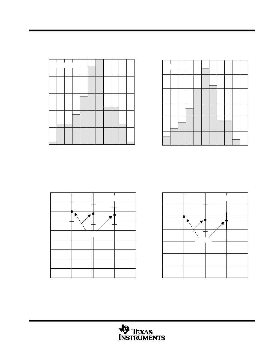
Figure 1
Number of
Amplifiers
DISTRIBUTION OF TPA4861
OUTPUT OFFSET VOLTAGE
20
10
0
VOO ş Output Offset Voltage ş mV
25
15
5
VDD = 5 V
ş4
ş3
ş2
ş1
0
1
2
3
4
5
6
Figure 2
Number of
Amplifiers
DISTRIBUTION OF TPA4861
OUTPUT OFFSET VOLTAGE
20
10
0
VOO ş Output Offset Voltage ş mV
25
15
5
ş4
ş3
ş2
ş1
0
1
2
3
4
5
6
VDD = 3.3 V
30
Figure 3
ş Supply Current ş mA
SUPPLY CURRENT DISTRIBUTION
vs
FREE-AIR TEMPERATURE
4
2.5
1.5
0.5
TA ş Free-Air Temperature ş
░
C
ş40
25
3
2
1
VDD = 5 V
I
DD
3.5
85
5
4.5
Typical
Figure 4
ş Supply Current ş mA
SUPPLY CURRENT DISTRIBUTION
vs
FREE-AIR TEMPERATURE
3.5
2
1
0
TA ş Free-Air Temperature ş
░
C
ş40
25
2.5
1.5
0.5
VDD = 3.3 V
I
DD
3
85
Typical