Please be aware that an important notice concerning availability, standard warranty, and use in critical applications of
Texas Instruments semiconductor products and disclaimers thereto appears at the end of this data sheet.
TPA0202
2-W STEREO AUDIO POWER AMPLIFIER
SLOS205A ş FEBRUARY 1998 ş REVISED MARCH 2000
1
POST OFFICE BOX 655303
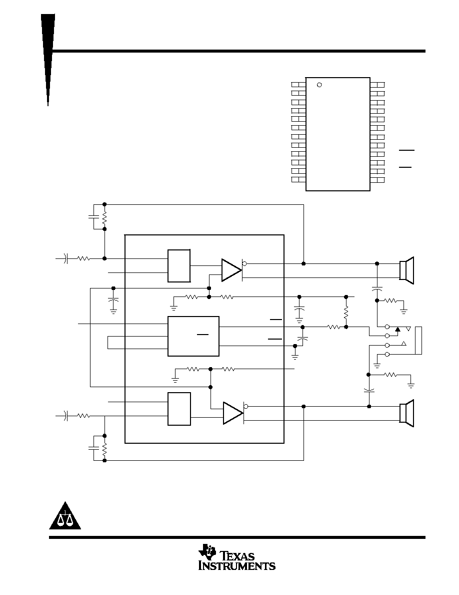
Ě
DALLAS, TEXAS 75265
D
Integrated Depop Circuitry
D
High Power with PC Power Supply
ş 2 W/Ch at 5 V into a 3-
Load
ş 800 mW/Ch at 3 V
D
Fully Specified for Use With 3-
Loads
D
Ultra-Low Distortion
ş 0.05% THD+N at 2 W and 3-
Load
D
Bridge-Tied Load (BTL) or Single-Ended
(SE) Modes
D
Stereo Input MUX
D
Surface-Mount Power Package
24-Pin TSSOP PowerPAD
TM
D
Shutdown Control . . . I
DD
= 5
Á
A
CB
CS
Right
MUX
RLINEIN
RHPIN
Left
MUX
LHPIN
LLINEIN
Bias, Mute,
Shutdown,
and SE/BTL
MUX Control
+
ş
+
ş
RBYPASS
MUTE IN
MUTE OUT
SHUTDOWN
LBYPASS
ROUT+
ROUT ş
RVDD
LVDD
LOUT+
LOUT ş
SE/BTL
HP/LINE
CIR
RIR
RFR
CFR
System
Control
CIL
RIL
NC
NC
4
5
6
8
9
11
19
20
21
RFL
CFL
100 k
100 k
VDD
VDD
COUTR
COUTL
10
3
16
7
14
18
15
22
1 k
1 k
1
2
3
4
5
6
7
8
9
10
11
12
24
23
22
21
20
19
18
17
16
15
14
13
GND/HS
TJ
LOUT+
LLINEIN
LHPIN
LBYPASS
LV
DD
SHUTDOWN
MUTE OUT
LOUTş
MUTE IN
GND/HS
GND/HS
NC
ROUT+
RLINEIN
RHPIN
RBYPASS
RV
DD
NC
HP/LINE
ROUTş
SE/BTL
GND/HS
PWP PACKAGE
(TOP VIEW)
Copyright
ę
2000, Texas Instruments Incorporated
PRODUCTION DATA information is current as of publication date.
Products conform to specifications per the terms of Texas Instruments
standard warranty. Production processing does not necessarily include
testing of all parameters.
PowerPAD is a trademark of Texas Instruments Incorporated.
TPA0202
2-W STEREO AUDIO POWER AMPLIFIER
SLOS205A ş FEBRUARY 1998 ş REVISED MARCH 2000
2
POST OFFICE BOX 655303
Ě
DALLAS, TEXAS 75265
description
The TPA0202 is a stereo audio power amplifier in a 24-pin TSSOP thermal package capable of delivering
greater than 2 W of continuous RMS power per channel into 3-
loads. The TPA0202 simplifies design and frees
up board space for other features. Full power distortion levels of less than 0.1% THD+N from a 5-V supply are
typical. Low-voltage applications are also well served by the TPA0202 providing 800-mW per channel into 3-
loads with a 3.3-V supply voltage.
The TPA0202 has integrated depop circuitry that virtually eliminates transients that cause noise in the speakers
during power up and when using the mute and shutdown modes.
Amplifier gain is externally configured by means of two resistors per input channel and does not require external
compensation for settings of 2 to 20 in BTL mode (1 to 10 in SE mode). An internal input MUX allows two sets
of stereo inputs to the amplifier. In notebook applications, where internal speakers are driven as BTL and the
line (often headphone drive) outputs are required to be SE, the TPA0202 automatically switches into SE mode
when the SE/BTL input is activated. Using the TPA0202 to drive line outputs up to 700 mW/channel into external
3-
loads is ideal for small non-powered external speakers in portable multimedia systems. The TPA0202 also
features a shutdown function for power sensitive applications, holding the supply current at 5
Á
A.
The PowerPAD package
(PWP) delivers a level of thermal performance that was previously achievable only
in TO-220-type packages. Thermal impedances of approximately 35
░
C/W are readily realized in multilayer PCB
applications. This allows the TPA0202 to operate at full power into 3-
loads at ambient temperature of up to
85
░
C with 300 CFM of forced-air cooling. Into 8-
loads, the operating ambient temperature increases to 100
░
C.
AVAILABLE OPTIONS
PACKAGE
TA
TSSOP
(PWP)
ş 40
░
C to 85
░
C
TPA0202PWP
The PWP packages are available taped and reeled. To order a taped
and reeled part, add the suffix R (e.g., TPA0202PWPR).
See Texas Instruments document, PowerPAD Thermally Enhanced Package Application Report (Literature Number SLMA002) for more
information on the PowerPAD package.
TPA0202
2-W STEREO AUDIO POWER AMPLIFIER
SLOS205A ş FEBRUARY 1998 ş REVISED MARCH 2000
3
POST OFFICE BOX 655303
Ě
DALLAS, TEXAS 75265
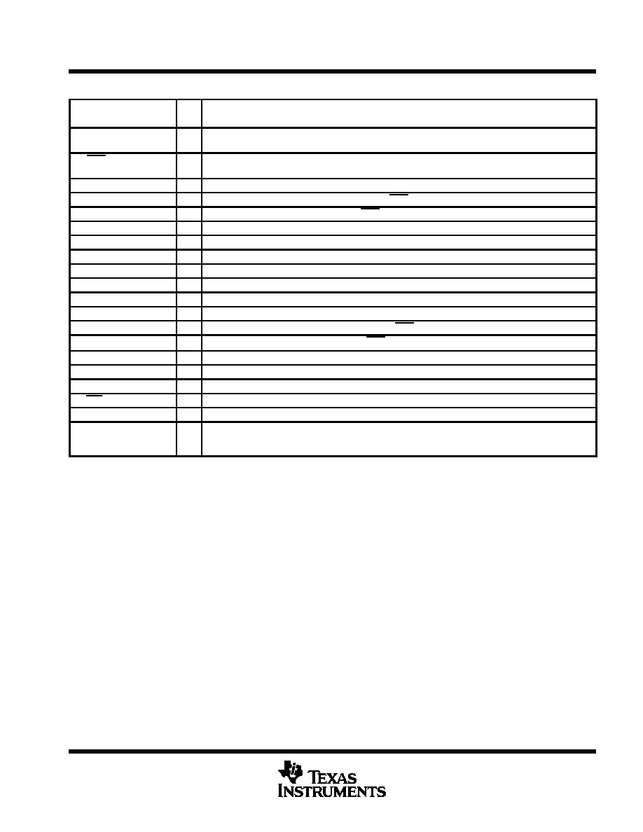
Terminal Functions
TERMINAL
I/O
DESCRIPTION
NAME
NO.
I/O
DESCRIPTION
GND/HS
1, 12,
13, 24
Ground connection for circuitry, directly connected to thermal pad
HP/LINE
16
I
Input MUX control input, hold high to select LHP IN or RHP IN (5, 20), hold low to select LLINE IN or
RLINE IN (4, 21)
LBYPASS
6
Tap to voltage divider for left channel internal mid-supply bias
LHP IN
5
I
Left channel headphone input, selected when HP/LINE terminal (16) is held high
LLINE IN
4
I
Left channel line input, selected when HP/LINE terminal (16) is held low
LOUT+
3
O
Left channel + output in BTL mode, + output in SE mode
LOUTş
10
O
Left channel ş output in BTL mode, high-impedance state in SE mode
LVDD
7
I
Supply voltage input for left channel and for primary bias circuits
MUTE IN
11
I
Mute all amplifiers, hold low for normal operation, hold high to mute
MUTE OUT
9
O
Follows MUTE IN terminal (11), provides buffered output
NC
17, 23
No internal connection
RBYPASS
19
Tap to voltage divider for right channel internal midşsupply bias
RHPIN
20
I
Right channel headphone input, selected when HP/LINE terminal (16) is held high
RLINEIN
21
I
Right channel line input, selected when HP/LINE terminal (16) is held low
ROUT+
22
O
Right channel + output in BTL mode, + output in SE mode
ROUTş
15
O
Right channel ş output in BTL mode, high impedance state in SE mode
RVDD
18
I
Supply voltage input for right channel
SE/BTL
14
I
Hold low for BTL mode, hold high for SE mode
SHUTDOWN
8
I
Places entire IC in shutdown mode when held high, IDD
= 5
Á
A
TJ
2
O
Sources a current proportional to the junction temperature. This terminal should be left unconnected
during normal operation. For more information, see the
junction temperature measurement section of
this document.
TPA0202
2-W STEREO AUDIO POWER AMPLIFIER
SLOS205A ş FEBRUARY 1998 ş REVISED MARCH 2000
4
POST OFFICE BOX 655303
Ě
DALLAS, TEXAS 75265
absolute maximum ratings over operating free-air temperature range (unless otherwise noted)
Supply voltage, V
DD
6 V
. . . . . . . . . . . . . . . . . . . . . . . . . . . . . . . . . . . . . . . . . . . . . . . . . . . . . . . . . . . . . . . . . . . . . . . .
Input voltage, V
I
ş0.3 V to V
DD
+0.3 V
. . . . . . . . . . . . . . . . . . . . . . . . . . . . . . . . . . . . . . . . . . . . . . . . . . . . . . . . . . . .
Continuous total power dissipation
internally limited (see Dissipation Rating Table)
. . . . . . . . . . . . . . . . . . . . .
Operating free-air temperature range, T
A
ş 40
░
C to 85
░
C
. . . . . . . . . . . . . . . . . . . . . . . . . . . . . . . . . . . . . . . . . . . .
Operating junction temperature range, T
J
ş 40
░
C to 150
░
C
. . . . . . . . . . . . . . . . . . . . . . . . . . . . . . . . . . . . . . . . . . .
Storage temperature range, T
stg
ş65
░
C to 150
░
C
. . . . . . . . . . . . . . . . . . . . . . . . . . . . . . . . . . . . . . . . . . . . . . . . . . .
Lead temperature 1,6 mm (1/16 inch) from case for 10 seconds
260
░
C
. . . . . . . . . . . . . . . . . . . . . . . . . . . . . . .
Stresses beyond those listed under "absolute maximum ratings" may cause permanent damage to the device. These are stress ratings only, and
functional operation of the device at these or any other conditions beyond those indicated under "recommended operating conditions" is not
implied. Exposure to absolute-maximum-rated conditions for extended periods may affect device reliability.
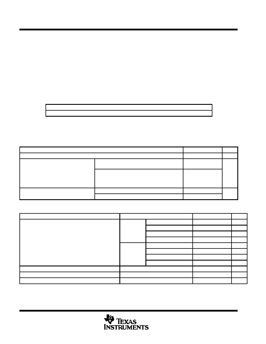
DISSIPATION RATING TABLE
PACKAGE
TA
25
░
C
DERATING FACTOR
TA = 70
░
C
TA = 85
░
C
PWP
2.7 W
21.8 mW/
░
C
1.7 W
1.4 W
Please see the Texas Instruments document, PowerPAD Thermally Enhanced Package Application Report
(literature number SLMA002), for more information on the PowerPAD package. The thermal data was
measured on a PCB layout based on the information in the section entitled
Texas Instruments Recommended
Board for PowerPAD on page 33 of the before mentioned document.
recommended operating conditions
MIN
NOM
MAX
UNIT
Supply Voltage, VDD
3
5
5.5
V
VDD = 5 V,
250 mW/ch average power,
4-
stereo BTL drive,
with proper PCB design
ş40
85
Operating free-air temperature, TA
VDD = 5 V,
2 W/ch average power,
3-
stereo BTL drive,
with proper PCB design
and 300 CFM forced-air
cooling
ş40
85
░
C
Common mode input voltage VICM
VDD = 5 V
1.25
4.5
V
Common mode input voltage, VICM
VDD = 3.3 V
1.25
2.7
V
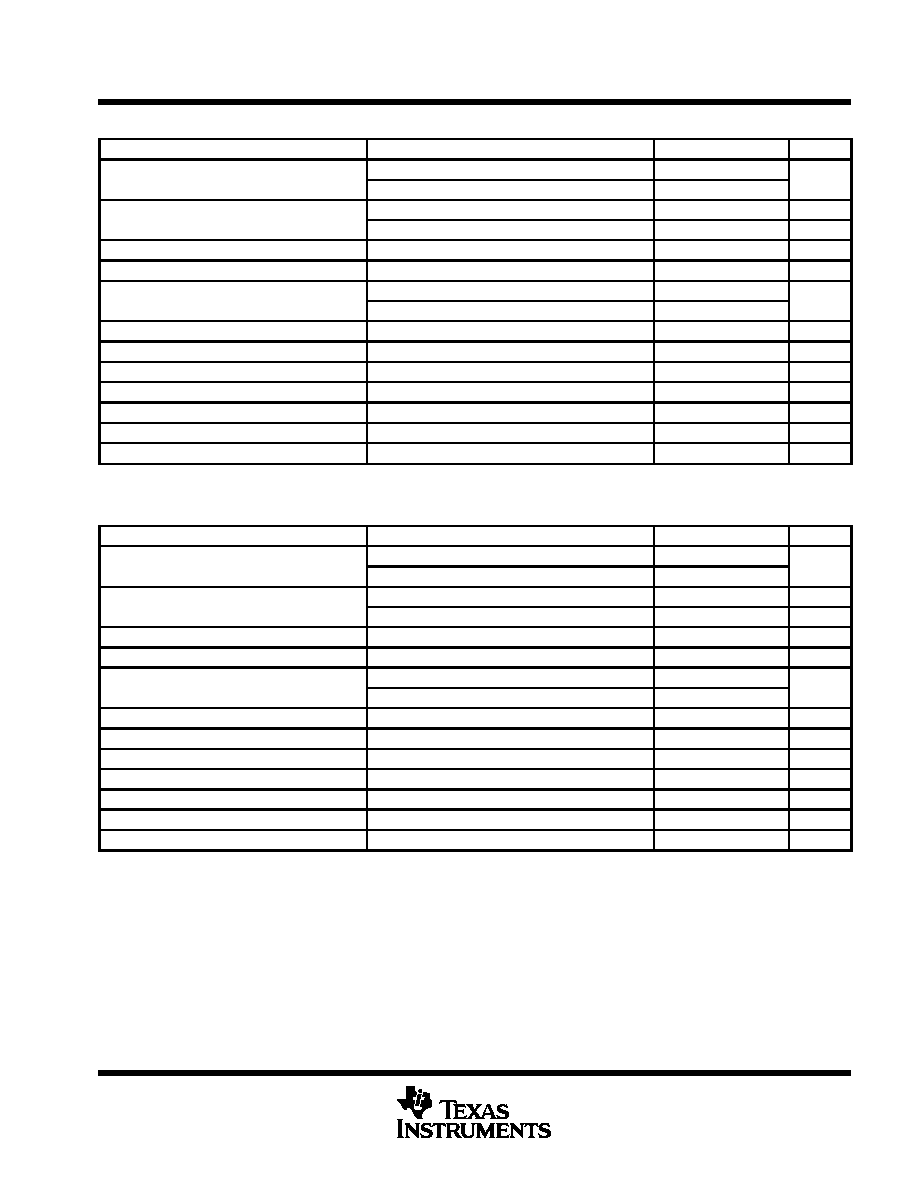
dc electrical characteristics, T
A
= 25
░
C
PARAMETER
TEST CONDITIONS
TYP
MAX
UNIT
Stereo BTL
19
25
mA
VDD = 5 V
Stereo SE
9
15
mA
VDD = 5 V
Mono BTL
9
15
mA
IDD
Supply current
Mono SE
3
10
mA
IDD
Supply current
Stereo BTL
13
20
mA
VDD = 3 3 V
Stereo SE
5
10
mA
VDD = 3.3 V
Mono BTL
5
10
mA
Mono SE
3
6
mA
VOO
Output offset voltage (measured differentially)
VDD = 5 V,
Gain = 2,
See Note 1
5
25
mV
IDD(MUTE) Supply current in mute mode
VDD = 5 V
1.5
mA
IDD(SD)
IDD in shutdown
VDD = 5 V
5
15
Á
A
NOTE 1: At 3 V < VDD < 5 V the dc output voltage is approximately VDD/2.
TPA0202
2-W STEREO AUDIO POWER AMPLIFIER
SLOS205A ş FEBRUARY 1998 ş REVISED MARCH 2000
5
POST OFFICE BOX 655303
Ě
DALLAS, TEXAS 75265
ac operating characteristics, V
DD
= 5 V, T
A
= 25
░
C, R
L
= 3
(unless otherwise noted)
PARAMETER
TEST CONDITIONS
TYP
MAX
UNIT
PO
Output power (each channel) see
THD = 0.2%,
BTL,
See Figure 3
2
W
PO
(
)
Note 2
THD = 1%,
BTL,
See Figure 3
2.2
W
THD+N
Total harmonic distortion plus noise
Po = 2W,
f = 20 ş 20 kHz,
See Figure 5
200
m%
THD+N
Total harmonic distortion plus noise
VI = 1 V,
RL = 10 k
,
AV = 1 V/V
100
m%
BOM
Maximum output power bandwidth
AV = 10 V/V
THD < 1 %,
See Figure 5
>20
kHz
Phase margin
RL = 4
,
Open Loop,
See Figure 43
85
░
Supply ripple rejection ratio
f = 1 kHz,
See Figure 37
80
dB
Supply ripple rejection ratio
f = 20 ş 20 kHz,
See Figure 37
60
dB
Mute attenuation
85
dB
Channel-to-channel output separation
f = 1 kHz,
See Figure 39
85
dB
Line/HP input separation
100
dB
BTL attenuation in SE mode
100
dB
ZI
Input impedance
2
M
Signal-to-noise ratio
Po = 500 mW,
BTL
95
dB
Vn
Output noise voltage
See Figure 35
21
Á
V(rms)
NOTE 2: Output power is measured at the output terminals of the IC at 1 kHz.
ac operating characteristics, V
DD
= 3.3 V, T
A
= 25
░
C, R
L
= 3
PARAMETER
TEST CONDITIONS
TYP
MAX
UNIT
PO
Output power (each channel) see
THD = 0.2%,
BTL,
See Figure 10
800
mW
PO
(
)
Note 2
THD = 1%,
BTL,
See Figure 10
900
mW
THD+N
Total harmonic distortion plus noise
Po = 800 mW,
f = 20 ş 20 kHz,
See Figure 11
350
m%
THD+N
Total harmonic distortion plus noise
VI = 1 V,
RL = 10 k
,
AV = 1 V/V
200
m%
BOM
Maximum output power bandwidth
AV = 10 V/V
THD < 1 %,
See Figure 11
>20
kHz
Phase margin
RL = 4
,
Open Loop,
See Figure 44
85
░
Supply ripple rejection ratio
f = 1 kHz,
See Figure 37
70
dB
Supply ripple rejection ratio
f = 20 ş 20 kHz,
See Figure 37
55
dB
Mute attenuation
85
dB
Channel-to-channel output separation
f = 1 kHz,
See Figure 40
85
dB
Line/HP input separation
100
dB
BTL attenuation in SE mode
100
dB
ZI
Input impedance
2
M
Signal-to-noise ratio
Po = 500 mW,
BTL
95
dB
Vn
Output noise voltage
See Figure 37
21
Á
V(rms)
NOTE 2: Output power is measured at the output terminals of the IC at 1 kHz.