TMS34094
ISA BUS INTERFACE
SPVS006A FEBRUARY 1992 REVISED JUNE 1992
POST OFFICE BOX 1443
·
HOUSTON, TEXAS 77001
1
Copyright
©
1992, Texas Instruments Incorpo-
rated
PRODUCTION DATA information is current as of publication
date. Products conform to specifications per the terms of Texas
Instruments standard warranty. Production processing does
not necessarily include testing of all parameters.
·
Simplifies Design of High-Performance ISA
PC Graphics Systems
·
Single-Integrated Circuit Interfaces
TMS34020 to ISA Bus
·
Conforms to ISA Portions of the EISA
Rev. 3.11 Specifications
·
Internal Data Bus Transceivers
·
Register Configurable I/O Mapped or
Memory-Mapped Interface
·
Register Configurable as an 8- or 16-Bit ISA
Memory-Mapped Device
·
Configurable TMS34020 Address Space
Decoding
VRAM Shift Register Transfer Decoding
VRAM Mask Write and VRAM Color
Register Write Access Decoding
·
VGA Passthrough Support
·
Operating Free-Air Temperature
. . . 0
°
C to 55
°
C
description
The TMS34094 ISA Bus Interface device, a peripheral device for the TMS34020 Graphics Processor, facilitates
the design of a high-performance graphics system for use in an ISA Bus-compatible PC. The device decodes
ISA Bus cycles and controls the TMS34020 host interface to enable read and write accesses to the TMS34020's
local memory. In addition, the TMS34094 allows the host to access the TMS34020's local memory via either
I/O-mapped or memory-mapped ISA Bus accesses. The capability is software configurable, simplifying design
and reducing system cost.
I/O mapped interface
The I/O mapped interface defines three I/O locations which facilitate access to the entire range of TMS34020
local memory. Two registers are used together to provide a 28-bit address to the TMS34020. The third register
acts as the data port between the ISA Bus and TMS34020 local memory. This set of three registers supports
the TMS34020's autoincrement modes which reduce data transfer overhead. For simplifying interrupt routines,
the TMS34094 also provides read back of the address for the next host access.
memory-mapped interface
The memory-mapped interface provides four highly configurable windows between host memory space and
TMS34020 memory space. Each window has four individually configurable attributes. These include: response
as either an 8-bit or 16-bit device; begin address in the memory map of the host; begin address in the memory
map of the TMS34020; and size. Size may range from 8K bytes to 4M bytes.
1
40
160
121
41
80
120
81
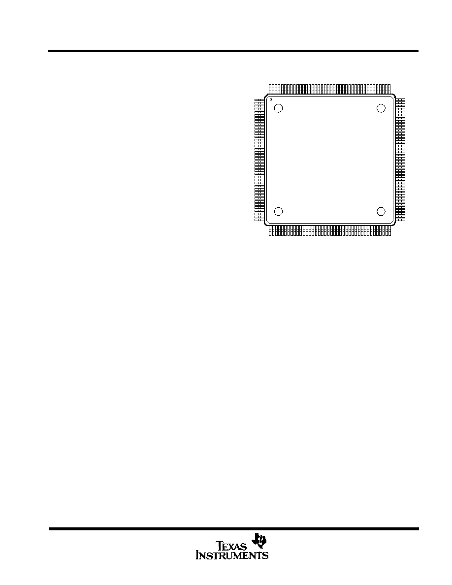
160-PIN PC PLASTIC QUAD-FLAT
PACKAGE (EIAJ)
(TOP VIEW)

TMS34094
ISA BUS INTERFACE
SPVS006A FEBRUARY 1992 REVISED JUNE 1992
POST OFFICE BOX 1443
·
HOUSTON, TEXAS 77001
2
local memory decode
TMS34020 local memory map decoding is provided by the TMS34094. The TMS34094 internally decodes LAD
bus addresses to generate four bank select output signals. The bank select signals may be used to control
DRAM, VRAM, ROM and other devices in the TMS34020 local memory map. This programmable decoding
allows designs to support multiple resolutions and color depths through software configuration.
For applications requiring synchronization of host software and TMS34020 software, the TMS34094 shadows
the TMS34020 host control register low (HSTCTLL) as an ISA I/O register. This eliminates a LAD bus host
access cycle, thereby reducing LAD bus traffic and increasing TMS34020 performance.
To simplify the design of VGA-compatible, single-monitor graphics systems, the TMS34094 supports VGA
passthrough. Onchip passthrough logic supports designs where VGA controllers are onboard, as well as
designs where a VGA-compatible auxiliary video connector is provided. The TMS34094 decodes ISA Bus
accesses to standard VGA palette control registers and signals that a VGA pass-through access is occurring.
Shadowing of VGA passthrough cycles may be disabled, enabled for writes only, or enabled for reads and
writes.
TMS34094
ISA BUS INTERFACE
SPVS006A FEBRUARY 1992 REVISED JUNE 1992
POST OFFICE BOX 1443
·
HOUSTON, TEXAS 77001
3
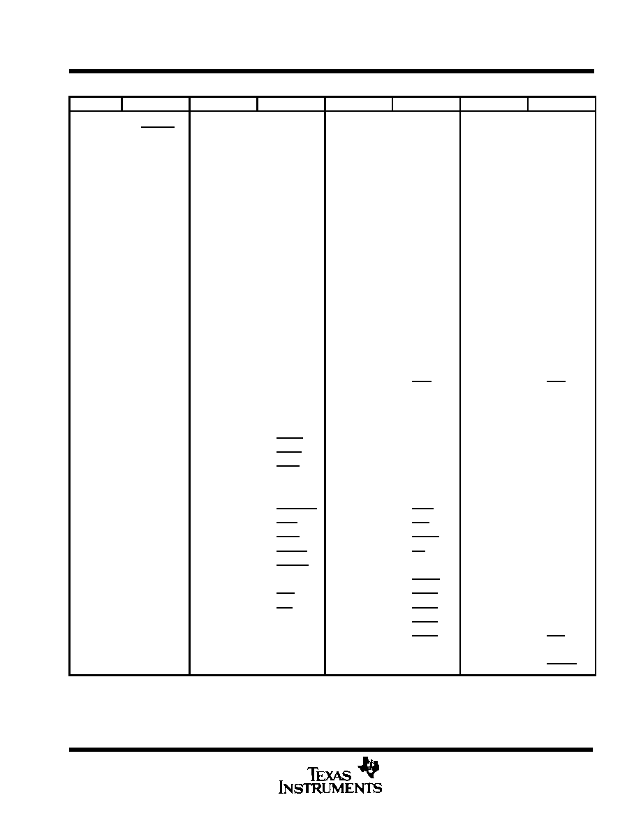
pin assignment
PIN NO.
NAME
PIN NO.
NAME
PIN NO.
NAME
PIN NO.
NAME
1
VSS
41
VSS
81
VSS
121
VSS
2
HWRITE
42
SA19
82
D14
122
SSRT
3
HBS01
43
SA18
83
D6
123
LAD31
4
HBS23
44
SA17
84
D13
124
LAD15
5
HA5
45
SA16
85
D5
125
LAD30
6
HA6
46
SA15
86
D12
126
LAD14
7
HA7
47
SA14
87
D4
127
LAD29
8
HA8
48
SA13
88
D11
128
LAD13
9
HA9
49
SA12
89
D3
129
LAD28
10
HA10
50
SA11
90
D10
130
LAD12
11
HA11
51
SA10
91
D2
131
LAD27
12
HA12
52
SA9
92
D9
132
LAD11
13
HA13
53
SA8
93
D1
133
LAD26
14
HA14
54
SA7
94
D8
134
LAD10
15
HA15
55
SA6
95
D0
135
LAD25
16
HA16
56
SA5
96
PCINT
136
LAD9
17
HA17
57
SA4
97
RESDRV
137
LAD24
18
HA18
58
SA3
98
BIOSEN
138
LAD8
19
VSS
59
VSS
99
VSS
139
VSS
20
HA19
60
SA2
100
HINT
140
HOE
21
VCC
61
VCC
101
VCC
141
VCC
22
HA20
62
SA1
102
IOSEL2
142
LAD23
23
HA21
63
SA0
103
IOSEL1
143
LAD7
24
HA22
64
MWTC
104
IOSEL0
144
LAD22
25
HA23
65
MRDC
105
HRDY
145
LAD6
26
HA24
66
SBHE
106
LCLK2
146
LAD21
27
HA25
67
BALE
107
LCLK1
147
LAD5
28
HA26
68
BCLK
108
HDST
148
LAD20
29
HA27
69
REFRESH
109
CAS2
149
LAD4
30
HA28
70
IORC
110
RAS
150
LAD19
31
HA29
71
IOWC
111
ALTCH
151
LAD3
32
HA30
72
SMRDC
112
WE
152
LAD18
33
HA31
73
SMWTC
113
SF
153
LAD2
34
LA17
74
AEN
114
RESET
154
LAD17
35
LA18
75
IO16
115
BSEL0
155
LAD1
36
LA19
76
M16
116
BSEL1
156
LAD16
37
LA20
77
CHRDY
117
BSEL2
157
LAD0
38
LA21
78
NC
118
BSEL3
158
HCS
39
LA22
79
D15
119
VCC
159
VCC
40
LA23
80
D7
120
VGASHD
160
HREAD
NC DO NOT CONNECT.

TMS34094
ISA BUS INTERFACE
SPVS006A FEBRUARY 1992 REVISED JUNE 1992
POST OFFICE BOX 1443
·
HOUSTON, TEXAS 77001
4
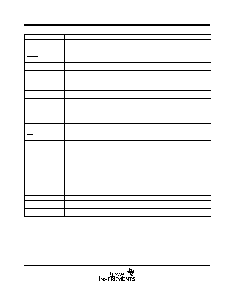
signal descriptions
SIGNAL
I/O/Z
TMS34020 INTERFACE SIGNALS
LCLK1, LCLK2
I
Local clocks. These signals are used to synchronize the access with the TMS34020.
LAD0LAD31
I/O
32-bit multiplexed local address/data bus. These signals are used to monitor the address and status of a
TMS34020 memory cycle and to read and write data from the TMS34094 to memory.
ALTCH
I
Address latch. The high-to-low transition of the signal indicates the address value on LAD0LAD31 is valid.
RAS
I
Row-address strobe. The row-address strobe from the TMS34020.
CAS2
I
Column-address strobe. This signal is used to indicate a possible access to the least significant byte of the
HSTCTLL register.
WE
I
Write enable. This signal from the TMS34020 is used to indicate a possible write access to the HSTCTLL register.
SF
I
VRAM special function. This signal from the TMS34020 is used in decoding LAD bus shift register transfer cycles
to control the shift clock insertion indicator signal SSRT.
HDST
I
Host data latch strobe. The rising edge of this signal latches data on LAD0LAD31 into the TMS34094 during
a host read of TMS34020 memory.
HOE
I
Host data output enable. Enables the TMS34094 to drive data onto LAD0LAD31 during a host write cycle.
HRDY
I
Host ready. This normally low signal is asserted high by the TMS34020 to indicate that the TMS34020 is ready
to complete a host-initiated cycle. It is used to generate the CHRDY output from the TMS34094.
HCS
O
Host chip select. This signal is driven low to latch the address presented on HA5HA31 into the TMS34020 and
initiate a host access cycle. The status of this signal also configures the TMS34020 for autoincrement access. A
pull-up resistor is required on HCS to ensure that the TMS34020 will reset to Host Present mode.
HREAD
O
Host read. This active low signal is driven low to indicate a read request from the ISA bus of TMS34020 local
memory.
HWRITE
O
Host write. This active low signal is driven low to indicate a write request of TMS34020 memory from the ISA Bus.
HA5HA31
O
27 host-address signals. The value represents the address of the 32-bit quantity being accessed in the
TMS34020 local memory.
HBS01
O
Host byte select 01. This signal is connected to both HBS0 and HBS1 of the TMS34020 to indicate that the host
requests an access to the even 16-bit word of the 32-bit quantity specified by HA5HA31.
HBS23
O
Host byte select 23. This signal is connected to both HBS2 and HBS3 of the TMS34020 to indicate that the host
requests an access to the odd 16-bit word of the 32-bit quantity specified by HA5HA31.
RESET
O
Subsystem reset. This signal indicates a reset to the graphics subsystem and should be connected to the RESET
input of the TMS34020 and the palette. RESET will become active low after the ISA signal RESDRV has
remained low for four consecutive cycles on LCLK1. It can also be asserted by setting the RS bit in the TMS34094
MODECTL register.
HINT
I
Host interrupt. This signal is connected to the TMS34020 HINT output. The PCINT output follows the inverse of
this input.
SIGNAL
I/O/Z
ISA INTERFACE SIGNALS
BCLK
I
Bus clock. This signal is used to synchronize some ISA Interface signals.
BALE
I
Bus address latch enable. The high state of this signal indicates that a valid address is presented on LA17LA31.
SA0SA19
I
20-bit system address bus. These signals form the low-order 20 bits of the 24-bit address supported by 16-bit
ISA systems.
LA17LA23
I
7-bit latchable address bus. These signals form the high-order 4 bits of the 24-bit ISA address. When the partial
address on LA17LA23 selects a 128 KB segment containing a TMS34094 memory map which is configured as
a 16-bit memory peripheral, M16 is generated. The inputs are internally pulled low and may be disconnected from
the bus. This allows the TMS34094 to be installed in an 8-bit expansion slot.
D0D15
I/O
16-bit data bus. These signals provide a 16-bit data path to the ISA host.
MRDC
I
Memory read command. This signal indicates that the TMS34094 should drive its data onto D0D15 for a valid
memory mapped read access. An internal pullup holds this input deasserted when the TMS34094 is installed in
an 8-bit expansion slot.
SMRDC
I
System memory read command. This signal has a similar function as MRDC but is only activated for accesses
to host memory addresses between 000000h and 0FFFFFh and for refresh cycles.
TMS34094
ISA BUS INTERFACE
SPVS006A FEBRUARY 1992 REVISED JUNE 1992
POST OFFICE BOX 1443
·
HOUSTON, TEXAS 77001
5
signal descriptions (concluded)
SIGNAL
I/O/Z
ISA INTERFACE SIGNALS (continued)
MWTC
I
Memory write command. This signal is asserted to indicate that the TMS34094 should latch the data from the
bus if a valid memory mapped access has been detected. The TMS34094 issues a host write request to the
TMS34020 after the valid data has been latched. An internal pullup holds this input deasserted when the
TMS34094 is installed in an 8-bit expansion slot.
SMWTC
I
System memory write command. This signal has a similar function as MWTC but is activated only for accesses
to host memory addresses between 000000h and 0FFFFFh.
IORC
I
I/O read command. This signal indicates that the TMS34094 should drive its data onto D0D15 if a valid I/O
mapped access has been detected.
IOWC
I
I/O write command. This signal indicates that the TMS34094 should latch data from D0D15 if a valid I/O access
has been detected.
SBHE
I
System byte high enable. This signal, when low, indicates that the TMS34094, if configured and installed as
a 16-bit peripheral, should drive or accept data on the high half of the data bus, D8D15. An internal pullup resis-
tor holds this input deasserted when the TMS34094 is installed in an 8-bit expansion slot.
AEN
I
Address enable. This signal indicates that the TMS34094 may respond to the I/O address and command pres-
ent on the bus, when AEN = 0.
REFRESH
I
ISA refresh. The low state of this signal indicates a refresh cycle is in progress in the ISA system. The TMS34094
ignores all ISA refresh cycles.
RESDRV
I
Reset drive. Assertion of RESDRV causes a reset of the TMS34094 and asserts the signal RESET low.
CHRDY
O
Channel ready. This is an open collector signal and is asserted whenever the TMS34094 must initiate an access
to the TMS34020 local memory. In response to an ISA access cycle it indicates that the access has to be
extended.
M16
O
16-bit memory data size. This open collector signal indicates a memory window configured as a 16-bit peripher-
al has been accessed through the TMS34094.
IO16
O
16-bit I/O data size. This open collector signal is asserted upon an access to any TMS34094 I/O register. There-
fore, 16-bit I/O data transfer will be used whenever the TMS34094 is installed in a 16-bit bus.
PCINT
O
PC interrupt request. This totem pole signal issues an interrupt request to the ISA host when it goes from a low
to a high state and remains there until the appropriate interrupt routine has been executed. It may be
connected directly to an IRQ signal on the ISA bus.
SIGNAL
I/O/Z
LOCAL BUS INTERFACE SIGNALS
BSEL0BSEL3
O
4 bank select controls. TheTMS34094 asserts these signals based on decoding of the LAD bus address and
the type of access. These signals are typically ORed with the RAS output of the TMS34020 for use as row ad-
dress strobes for four banks of memory.
SSRT
O
Shift register transfer indicator. This active high signal may be used to indicate to the video backend logic
(such as the TLC34075) that a shift register transfer has occurred and that an inserted or relocated SCLK pulse
should be triggered. This output is typically used only in systems which use VRAMs which require an SCLK pulse
between a normal shift register transfer and a split shift register transfer and which enables the TMS34020s gen-
eration of split shift register transfers.
VGASHD
O
VGA shadow indicator. This active high signal precedes the TMS34020 host cycle caused by a VGA palette
access to alert the palette access control logic of a VGA palette access on the ISA bus.
SIGNAL
I/O/Z
CONFIGURATION INTERFACE
IOSEL0IOSEL2
I
I/O base select pins. Input from these pins selects the base I/O range in ISA space in which the TMS34094 I/O
registers appear.
BIOSEN
I
BIOS ROM enable pin. Setting this input high maps the BIOS ROM in the TMS34020 local memory into ISA
space after reset.