
TMS320LF2407, TMS320LF2406, TMS320LF2402
TMS320LC2406, TMS320LC2404, TMS320LC2402
DSP CONTROLLERS
SPRS094C Ł APRIL 1999 Ł REVISED OCTOBER 1999
1
POST OFFICE BOX 1443
Ę
HOUSTON, TEXAS 77251Ł1443
D
High-Performance Static CMOS Technology
Ł 33-ns Instruction Cycle Time (30 MHz)
Ł 30 MIPS Performance
Ł Low-Power 3.3-V Design
D
Based on T320C2xx DSP CPU Core
Ł Code-Compatible With 'F243/'F241/'C242
Ł Instruction Set and Module Compatible
With 'F240/'C240
Ł Source-Code-Compatible With
TMS320C1x/2x
D
Flash (LF) and ROM (LC) Device Options
Ł 'LF240x
: 'LF2407, 'LF2406, 'LF2402
Ł 'LC240x
: 'LC2406, 'LC2404, 'LC2402
D
On-Chip Memory
Ł Up to 32K Words x 16 Bits of Flash
EEPROM (4 Sectors) or ROM
Ł Up to 2.5K Words x 16 Bits of
Data/Program RAM
Ł 544 Words of Dual-Access (DARAM)
Ł 2K Words of Single-Access (SARAM)
D
Boot ROM ('LF240x Devices)
Ł SCI/SPI Flash Bootloader
D
Two Event-Manager (EV) Modules (A and B)
EVA and EVB Each Include:
Ł Two 16-Bit General-Purpose Timers
Ł Eight 16-Bit Pulse-Width Modulation
(PWM) Channels Which Enable:
Ł Three-Phase Inverter Control
Ł Centered or Edge Alignment of PWM
Channels
Ł Emergency PWM Channel Shutdown
With External PDPINT Pin
Ł Programmable Deadband Prevents
Shoot-Through Faults
Ł Three Capture Units For Time-Stamping
of External Events
Ł On-Chip Position Encoder Interface
Circuitry
Ł Synchronized Analog-to-Digital
Conversion
Ł Suitable for AC Induction, BLDC,
Switched Reluctance, and Stepper Motor
Control
Ł Applicable for Multiple Motor and/or
Converter Control
D
External Memory Interface ('LF2407)
Ł 192K Words x 16 Bits of Total Memory,
64K Program, 64K Data, 64K I/O
D
Watchdog (WD) Timer Module
D
10-Bit Analog-to-Digital Converter (ADC)
Ł 8 or 16 Multiplexed Input Channels
Ł 500 ns Minimum Conversion Time
Ł Selectable Twin 8-Input Sequencers
Triggered by Two Event Managers
D
Controller Area Network (CAN) 2.0B Module
D
Serial Communications Interface (SCI)
D
16-Bit Serial Peripheral Interface (SPI)
Module (Except 'x2402)
D
Phase-Locked-Loop (PLL)-Based Clock
Generation
D
Up to 40 Individually Programmable,
Multiplexed General-Purpose Input / Output
(GPIO) Pins
D
Five External Interrupts (Power Drive
Protection, Reset, and Two Maskable
Interrupts)
D
Power Management:
Ł Three Power-Down Modes
Ł Ability to Power-Down Each Peripheral
Independently
D
Real-Time JTAG-Compliant Scan-Based
Emulation, IEEE Standard 1149.1
(JTAG)
D
Development Tools Include:
Ł Texas Instruments (TI
TM
) ANSI
C Compiler, Assembler / Linker, and
Code Composer
TM
Debugger
Ł Evaluation Modules
Ł Scan-Based Self-Emulation (XDS510
TM
)
Ł Numerous Third-Party Digital Motor
Control Support
D
Package Options
Ł 144-Pin Thin Quad Flatpack (TQFP) PGE
('LF2407)
Ł 100-Pin TQFP PZ ('LC2404, 'LC2406,
'LF2406)
Ł 64-Pin PQFP PG ('LC2402 and 'LF2402)
D
Extended Temperature Options (A and S)
Ł A: Ł 40
░
C to 85
░
C
Ł S: Ł 40
░
C to 125
░
C
ADV
ANCE
INFORMA
TION
Copyright
®
1999, Texas Instruments Incorporated
Please be aware that an important notice concerning availability, standard warranty, and use in critical applications of
Texas Instruments semiconductor products and disclaimers thereto appears at the end of this data sheet.
TI, Code Composer, and XDS510 are trademarks of Texas Instruments Incorporated.
Throughout this data sheet, '240x is used as a generic name for the 'LF240x/'LC240x family of devices.
IEEE Standard 1149.1Ł1990, IEEE Standard Test-Access Port
ADVANCE INFORMATION concerns new products in the sampling or
preproduction phase of development. Characteristic data and other
specifications are subject to change without notice.

TMS320LF2407, TMS320LF2406, TMS320LF2402
TMS320LC2406, TMS320LC2404, TMS320LC2402
DSP CONTROLLERS
SPRS094C Ł APRIL 1999 Ł REVISED OCTOBER 1999
2
POST OFFICE BOX 1443
Ę
HOUSTON, TEXAS 77251Ł1443
Description
2
. . . . . . . . . . . . . . . . . . . . . . . . . . . . . . . . . . . . .
TMS320x240x Device Summary
3
. . . . . . . . . . . . . . . . . . .
Functional Block Diagram of the '2407 DSP Controller 4
Pin Functions
8
. . . . . . . . . . . . . . . . . . . . . . . . . . . . . . . . . . .
Memory Maps
15
. . . . . . . . . . . . . . . . . . . . . . . . . . . . . . . . .
Peripheral Memory Map of the 'LF240x/'LC240x
21
. . . .
Device Reset and Interrupts
22
. . . . . . . . . . . . . . . . . . . . .
TMS320x240x Instruction Set
26
. . . . . . . . . . . . . . . . . . . .
Functional Block Diagram
of the '240x DSP CPU
27
. . .
Peripherals
36
. . . . . . . . . . . . . . . . . . . . . . . . . . . . . . . . . . . .
Event Manager Modules (EVA, EVB)
36
. . . . . . . . . . . .
Enhanced Analog-to-Digital Converter
(ADC) Module
40
. . . . . . . . . . . . . . . . . . . . . . . . . . . .
Controller Area Network (CAN) Module
41
. . . . . . . . . .
Serial Communications Interface (SCI) Module
44
. . . .
Serial Peripheral Interface (SPI) Module
46
. . . . . . . . . .
PLL-Based Clock Module
48
. . . . . . . . . . . . . . . . . . . . . .
Digital I/O and Shared Pin Functions
51
. . . . . . . . . . . . .
External Memory Interface ('LF2407)
54
. . . . . . . . . . . .
Watchdog (WD) Timer Module
55
. . . . . . . . . . . . . . . . . .
Development Support
58
. . . . . . . . . . . . . . . . . . . . . . . . . . .
Documentation Support
61
. . . . . . . . . . . . . . . . . . . . . . . . .
Absolute Maximum Ratings
62
. . . . . . . . . . . . . . . . . . . . . .
Recommended Operating Conditions
62
. . . . . . . . . . . . .
Peripheral Register Description
90
. . . . . . . . . . . . . . . . . . .
Mechanical Data
103
. . . . . . . . . . . . . . . . . . . . . . . . . . . . . .
Table of Contents
description
The TMS320LF240x and TMS320LC240x devices, new members of the '24x family of digital signal processor
(DSP) controllers, are part of the C2000 platform of fixed-point DSPs. The '240x devices offer the enhanced
TMS320 architectural design of the 'C2xx core CPU for low-cost, low-power, high-performance processing
capabilities. Several advanced peripherals, optimized for digital motor and motion control applications, have
been integrated to provide a true single chip DSP controller. While code-compatible with the existing '24x DSP
controller devices, the '240x offers increased processing performance (30 MIPS) and a higher level of peripheral
integration. See the TMS320x240x device summary section for device-specific features.
The '240x family offers an array of memory sizes and different peripherals tailored to meet the specific
price/performance points required by various applications. Flash-based devices of up to 32K words offer a
reprogrammable solution useful for:
Ł
Applications requiring field programmability upgrades
Ł
Development and initial prototyping of applications that migrate to ROM-based devices
Flash devices and corresponding ROM devices are fully pin-to-pin compatible. Note that flash-based devices
contain a 256-word boot ROM to facilitate in-circuit programming.
All '240x devices offer at least one event manager module which has been optimized for digital motor control
and power conversion applications. Capabilities of this module include centered- and/or edge-aligned PWM
generation, programmable deadband to prevent shoot-through faults, and synchronized analog-to-digital
conversion. Devices with dual event managers enable multiple motor and/or converter control with a single
'240x DSP controller.
The high performance, 10-bit analog-to-digital converter (ADC) has a minimum conversion time of 500 ns and
offers up to 16 channels of analog input. The auto sequencing capability of the ADC allows a maximum of
16 conversions to take place in a single conversion session without any CPU overhead.
A serial communications interface (SCI) is integrated on all devices to provide asynchronous communication
to other devices in the system. For systems requiring additional communication interfaces; the '2407, '2406,
and '2404 offer a 16-bit synchronous serial peripheral interface (SPI). The '2407 and '2406 offer a controller area
network (CAN) communications module that meets 2.0B specifications. To maximize device flexibility,
functional pins are also configurable as general purpose inputs/outputs (GPIO).
To streamline development time, JTAG-compliant scan-based emulation has been integrated into all devices.
This provides non-intrusive real-time capabilities required to debug digital control systems. A complete suite
of code generation tools from C compilers to the industry-standard Code Composer debugger supports this
family. Numerous third party developers not only offer device-level development tools, but also system-level
design and development support.
ADV
ANCE
INFORMA
TION
TMS320LF2407, TMS320LF2406, TMS320LF2402
TMS320LC2406, TMS320LC2404, TMS320LC2402
DSP CONTROLLERS
SPRS094C Ł APRIL 1999 Ł REVISED OCTOBER 1999
3
POST OFFICE BOX 1443
Ę
HOUSTON, TEXAS 77251Ł1443
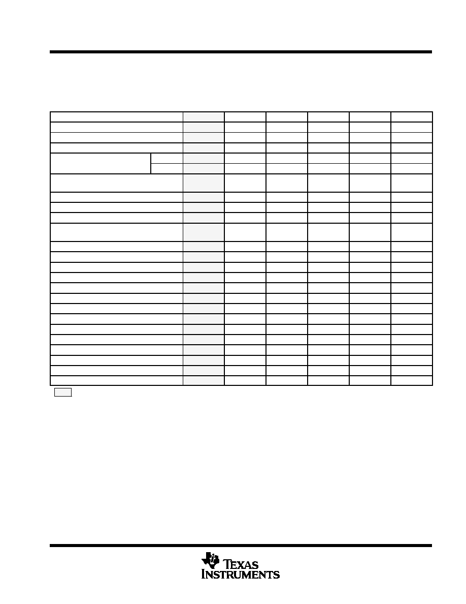
TMS320x240x device summary
Note that throughout this data sheet, '240x is used as a generic name for the 'LF240x/'LC240x family of devices.
Table 1. Hardware Features of '240x Devices
FEATURE
'LF2407
'LF2406
'LF2402
'LC2406
'LC2404
'LC2402
'C2xx DSP Core
Yes
Yes
Yes
Yes
Yes
Yes
Instruction Cycle
33 ns
33 ns
33 ns
33 ns
33 ns
33 ns
MIPS (30 MHz)
30 MIPS
30 MIPS
30 MIPS
30 MIPS
30 MIPS
30 MIPS
RAM (16 bit word)
DARAM
544
544
544
544
544
544
RAM (16-bit word)
SARAM
2K
2K
--
2K
1K
--
On-chip Flash (16-bit word)
(4 sectors: 4K, 12K, 12K, 4K)
32K
32K
8K
--
--
--
On-chip ROM (16-bit word)
--
--
--
32K
16K
4K
Boot ROM (16-bit word)
256
256
256
--
--
--
External Memory Interface
Yes
--
--
--
--
--
Event Managers A and B
(EVA and EVB)
EVA, EVB
EVA, EVB
EVA
EVA, EVB
EVA, EVB
EVA
S
General-Purpose (GP) Timers
4
4
2
4
4
2
S
Compare (CMP)/PWM
10/16
10/16
5/8
10/16
10/16
5/8
S
Capture (CAP)/QEP
6/4
6/4
3/2
6/4
6/4
3/2
Watchdog Timer
Yes
Yes
Yes
Yes
Yes
Yes
10-Bit ADC
Yes
Yes
Yes
Yes
Yes
Yes
S
Channels
16
16
8
16
16
8
S
Conversion Time (minimum)
500 ns
500 ns
500 ns
500 ns
500 ns
500 ns
SPI
Yes
Yes
--
Yes
Yes
--
SCI
Yes
Yes
Yes
Yes
Yes
Yes
CAN
Yes
Yes
--
Yes
--
--
Digital I/O Pins (Shared)
41
41
21
41
41
21
External Interrupts
5
5
3
5
5
3
Supply Voltage
3.3 V
3.3 V
3.3 V
3.3 V
3.3 V
3.3 V
Packaging
144 TQFP
100 TQFP
64 PQFP
100 TQFP
100 TQFP
64 PQFP
'LF2407, the full-featured device of the 'LF240x family of DSP controllers, is useful for emulation and code development.
ADV
ANCE
INFORMA
TION

TMS320LF2407, TMS320LF2406, TMS320LF2402
TMS320LC2406, TMS320LC2404, TMS320LC2402
DSP CONTROLLERS
SPRS094C Ł APRIL 1999 Ł REVISED OCTOBER 1999
4
POST OFFICE BOX 1443
Ę
HOUSTON, TEXAS 77251Ł1443
functional block diagram of the '2407 DSP controller
XTAL1/CLKIN
XTAL2
PLLVCCA
PLLF2
PLLF
VSSA
VREFHI
ADCIN08ŁADCIN15
VCCA
ADCIN00ŁADCIN07
SCIRXD/IOPA1
SPISIMO/IOPC2
XINT2/ADCSOC/IOPD0
SCITXD/IOPA0
VREFLO
VCCP(5V)
Port A(0Ł7) IOPA[0:7]
SPICLK/IOPC4
SPISTE/IOPC5
SPISOMI/IOPC3
Port E(0Ł7) IOPE[0:7]
Port F(0Ł6) IOPF[0:6]
Port C(0Ł7) IOPC[0:7]
Port D(0) IOPD[0]
Port B(0Ł7) IOPB[0:7]
TDO
TDI
CANRX/IOPC7
TRST
CANTX/IOPC6
EMU1
PDPINTB
TCK
EMU0
TMS
CAP5/QEP4/IOPF0
CAP4/QEP3/IOPE7
PWM7/IOPE1
PWM8/IOPE2
CAP6/IOPF1
PWM10/IOPE4
PWM9/IOPE3
PWM11/IOPE5
PWM12/IOPE6
T4PWM/T4CMP/IOPF3
T3PWM/T3CMP/IOPF2
TDIRB/IOPF4
TCLKINB/IOPF5
DARAM (B0)
256 Words
DARAM (B1)
256 Words
DARAM (B2)
32 Words
'C2xx
DSP
Core
PLL Clock
10-Bit ADC
(With Twin
Autosequencer)
╚╚╚╚╚╚╚
╚╚╚╚╚╚╚
╚╚╚╚╚╚╚
╚╚╚╚╚╚╚
╚╚╚╚╚╚╚
╚╚╚╚╚╚╚
╚╚╚╚╚╚╚
╚╚╚╚╚╚╚
╚╚╚╚╚╚╚
╚╚╚╚╚╚╚
╚╚╚╚╚╚╚
╚╚╚╚╚╚╚
╚╚╚╚╚╚╚
╚╚╚╚╚╚╚
╚╚╚╚╚╚╚
╚╚╚╚╚╚╚
╚╚╚╚╚╚╚
╚╚╚╚╚╚╚
╚╚╚╚╚╚╚
╚╚╚╚╚╚╚
╚╚╚╚╚╚╚
╚╚╚╚╚╚╚
╚╚╚╚╚╚╚
RS
CLKOUT/IOPE0
XINT1/IOPA2
XINT2/ADCSOC/IOPD0
BIO/IOPC1
MP/MC
TMS2
A0ŁA15
D0ŁD15
TP1
TP2
BOOT_EN/XF
READY
STRB
R/W
RD
PS, DS, IS
VIS_OE
ENA_144
WE
CAP3/IOPA5
PWM1/IOPA6
CAP1/QEP1/IOPA3
CAP2/QEP2/IOPA4
PDPINTA
PWM5/IOPB2
PWM6/IOPB3
PWM3/IOPB0
PWM4/IOPB1
PWM2/IOPA7
T2PWM/T2CMP/IOPB5
T1PWM/T1CMP/IOPB4
TCLKINA/IOPB7
TDIRA/IOPB6
VDD (3.3 V)
VSS
VCCP(5V)
╚╚╚╚╚╚╚
╚╚╚╚╚╚╚
╚╚╚╚╚╚╚
╚╚╚╚╚╚╚
╚╚╚╚╚╚╚
╚╚╚╚╚╚╚
╚╚╚╚╚╚╚
╚╚╚╚╚╚╚
╚╚╚╚╚╚╚
SARAM (2K Words)
Flash/ROM
(32K Words:
4K/12K/12K/4K)
External Memory Interface
Event Manager A
D
3
ū
Capture Input
D
6
ū
Compare/PWM
Output
D
2
ū
GP Timers/PWM
SCI
SPI
WD
Digital I/O
(Shared With Other Pins)
CAN
JTAG Port
Event Manager B
D
3
ū
Capture Input
D
6
ū
Compare/PWM
Output
D
2
ū
GP Timers/PWM
╚╚╚
╚╚╚
╚╚╚
Indicates optional modules
The memory size and peripheral selection of these modules change for different '240x devices. See
Table 1 for device-specific details.
W/R / IOPC0
ADV
ANCE
INFORMA
TION

TMS320LF2407, TMS320LF2406, TMS320LF2402
TMS320LC2406, TMS320LC2404, TMS320LC2402
DSP CONTROLLERS
SPRS094C Ł APRIL 1999 Ł REVISED OCTOBER 1999
5
POST OFFICE BOX 1443
Ę
HOUSTON, TEXAS 77251Ł1443
144
143
142
141
140
139
138
137
136
135
134
RS
133
132
131
130
129
128
127
126
125
124
123
122
121
120
11
9
11
8
11
7
11
6
11
5
11
4
11
3
11
2
37
38
39
40
41
42
43
44
45
46
47
48
49
50
51
52
53
54
55
56
57
58
59
60
61
62
63
64
65
66
67
68
69
1
2
3
4
5
6
7
8
9
10
11
12
13
14
15
16
17
18
19
20
21
22
23
24
25
26
27
28
29
30
31
32
33
34
35
36
108
107
106
105
104
103
102
101
100
99
98
97
96
95
94
93
92
91
90
89
88
87
86
85
84
83
82
81
80
79
78
77
76
75
74
73
111
11
0
109
70
71
72
TMS320LF2407
PDPINTA
PLLF
TDIRA/
IOPB6
XINT2/ADCSOC/
IOPD0
CLKOUT/IOPE0
PDPINTB
XT
AL1/CLKIN
XT
AL2
PLLV
CCA
PLLF2
BOOT_EN/XF
CCP
V
TP1
TP2
IOPF6
EMU0
EMU1/OFF
TCK
TDI
TDO
TMS
TMS2
TRST
DS
IS
PS
R/W
W/R/IOPC0
RD
WE
STRB
READY
MP/MC
ENA_144
VIS_OE
A0
A1
A2
A3
A4
A5
A6
A7
A8
A9
A10
A1
1
A12
A13
A14
A15
D0
D1
D2
D3
D4
D5
D6
D7
D8
D9
D10
D11
D12
D13
D14
D15
PLLV
CCA
V
DD
DD
V
V
DD
DD
V
V
DDO
DDO
V
DDO
V
V
DDO
V
DDO
DDO
V
V
SS
SS
V
V
SS
SS
V
V
SSO
SSO
V
SSO
V
V
SSO
V
SSO
SSO
V
SSO
V
CAP1/QEP1/
IOPA3
CAP2/QEP2/
IOPA4
CAP3/
IOPA5
PWM1/
PWM2/
PWM3/
PWM4/
PWM5/
PWM6/
T1PWM/T1CMP/
IOPB4
T2PWM/T2CMP/
IOPB5
TCLKINA/
CAP4/QEP3/
IOPE7
CAP5/QEP4/
IOPF0
CAP6/
PWM7/
PWM8/
PWM9/
PWM10/
PWM1
1/
PWM12/
T3PWM/T3CMP/
IOPF2
T4PWM/T4CMP/
IOPF3
TDIRB/
IOPF4
TCLKINB/
ADCIN00
ADCIN01
ADCIN02
ADCIN03
ADCIN04
ADCIN05
ADCIN06
ADCIN07
ADCIN08
ADCIN09
ADCIN10
ADCIN11
ADCIN12
ADCIN13
ADCIN14
ADCIN15
REFHI
V
REFLO
V
CCA
V
SSA
V
CANRX/
CANTX/
SCITXD/
IOPA0
SCIRXD/
IOPA1
SPICLK/
IOPC4
SPISIMO/
IOPC2
SPISOMI/
IOPC3
SPISTE/
IOPC5
XINT1/
IOPA2
Bold, italicized pin names indicate pin function after reset.
BOOT_EN is available only on flash devices.
IOPB7
IOPE6
IOPB3
IOPB2
IOPE5
IOPB1
IOPB0
IOP
A
7
IOPE4
IOP
A
6
IOPE3
IOPE2
IOPE1
IOPF1
IOPC7
IOPC6
IOPF5
IOPC1
BIO/
PGE PACKAGE
(TOP VIEW)
ADV
ANCE
INFORMA
TION