TMS320F2810, TMS320F2812
DIGITAL SIGNAL PROCESSORS
SPRS174B Ł APRIL 2001 Ł REVISED SEPTEMBER 2001
1
POST OFFICE BOX 1443
Ę
HOUSTON, TEXAS 77251Ł1443
D
High-Performance Static CMOS Technology
Ł 150 MHz (6.67-ns Cycle Time)
Ł Low-Power (1.8-V Core, 3.3-V I/O) Design
Ł 3.3-V Flash Programming Voltage
D
High-Performance CPU (C28x)
Ł 16 x 16 and 32 x 32 MAC Operations
Ł 16 x 16 Dual MAC
Ł Harvard Bus Architecture
Ł Atomic Operations
Ł Fast Interrupt Response and Processing
Ł Unified Memory Programming Model
Ł 4M Linear Program Address Reach
Ł 4G Linear Data Address Reach
Ł Code-Efficient (in C/C++ and Assembly)
Ł TMS320F24x/LF240x Processor Source
Code Compatible
D
On-Chip Memory
Ł Up to 128K x 16 Flash
(8 x 4K and 6 x 16K Sectors)
Ł 2K x 16 OTP ROM
Ł L0 and L1: 2 Blocks of 4K x 16
Single-Access RAM (SARAM)
Ł H0: 1 Block of 8K x 16 SARAM
Ł M0 and M1: 2 Blocks of 1K x 16 SARAM
D
Boot ROM (4K x 16)
Ł With Software Boot Modes
Ł Standard Math Tables
D
External Interface (F2812)
Ł Up to 1.5M Total Memory
Ł Programmable Wait States
Ł Programmable Read/Write Strobe Timing
Ł Four Individual Chip Selects
D
Clock and System Control
Ł Dynamic PLL Ratio Changes Supported
Ł On-Chip Oscillator
Ł Watchdog Timer Module
D
Three External Interrupts
D
Peripheral Interrupt Expansion (PIE) Block
That Supports 45 Peripheral Interrupts
D
128-Bit Security Key/Lock
Ł Protects Flash/OTP and L0/L1 SARAM
Ł Prevents Firmware Reverse Engineering
D
Motor Control Peripherals
Ł Two Event Managers (EVA, EVB)
Ł Compatible to 240x Devices
D
Three 32-Bit CPU-Timers
D
Serial Port Peripherals
Ł Serial Peripheral Interface (SPI)
Ł Two Serial Communications Interfaces
(SCIs), Standard UART
Ł Enhanced Controller Area Network
(eCAN)
Ł Multichannel Buffered Serial Port
(McBSP) With SPI Mode
D
12-Bit ADC, 16 Channels
Ł 2 x 8 Channel Input Multiplexer
Ł Two Sample-and-Hold
Ł Single Conversion Time: 200 ns
Ł Pipeline Conversion Time: 60 ns
D
Up to 56 Individually Programmable,
Multiplexed General-Purpose Input / Output
(GPIO) Pins
D
Advanced Emulation Features
Ł Analysis and Breakpoint Functions
Ł Real-Time Debug via Hardware
D
Development Tools Include
Ł ANSI C/C++ Compiler/Assembler/Linker
Ł Supports TMS320C24x
/240x
Instructions
Ł Code Composer Studio
IDE
Ł DSP BIOS
Ł JTAG Scan Controllers
(TI or Third-Party)
Ł Evaluation Modules
Ł Broad Third-Party Digital Motor Control
Support
D
Low-Power Modes and Power Savings
Ł IDLE, STANDBY, HALT Modes Supported
Ł Disable Individual Peripheral Clocks
D
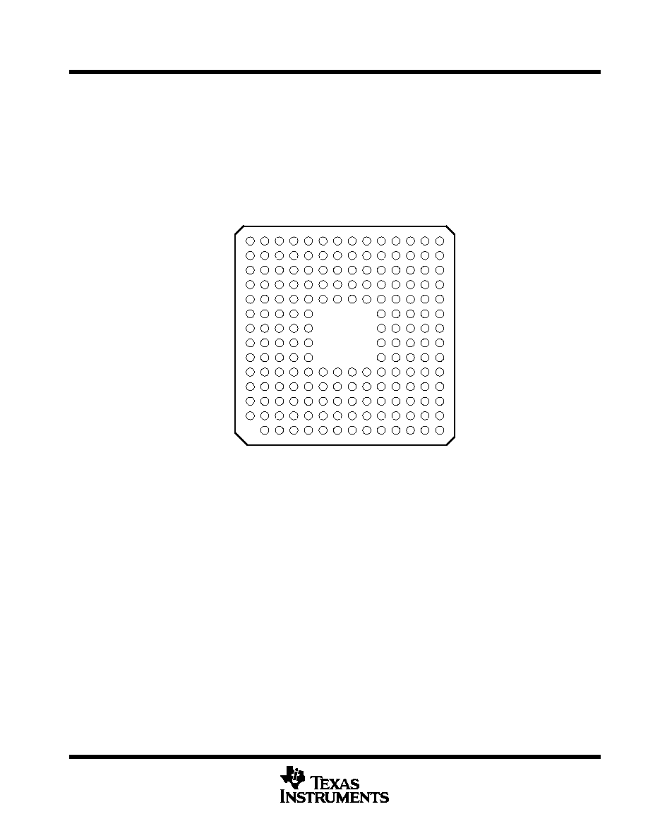
Package Options
Ł 179-Pin MicroStar BGA
With External
Interface (GHH) (F2812)
Ł 176-Pin Low-Profile Quad Flatpack
(LQFP) With External Interface (PGF)
(F2812)
Ł 128-Pin LQFP Without External Interface
(PBK) (F2810)
D
Temperature Options:
Ł A: Ł40
░
C to 85
░
C
Ł S: Ł40
░
C to 125
░
C
PR
O
DU
C
T PREVIEW
Copyright
2001, Texas Instruments Incorporated
Please be aware that an important notice concerning availability, standard warranty, and use in critical applications of
Texas Instruments semiconductor products and disclaimers thereto appears at the end of this data sheet.
TMS320C24x, Code Composer Studio, and MicroStar BGA are trademarks of Texas Instruments.
All trademarks are the property of their respective owners.
IEEE Standard 1149.1Ł1990, IEEE Standard Test-Access Port
PRODUCT PREVIEW information concerns products in the formative or
design phase of development. Characteristic data and other
specifications are design goals. Texas Instruments reserves the right to
change or discontinue these products without notice.

TMS320F2810, TMS320F2812
DIGITAL SIGNAL PROCESSORS
SPRS174B Ł APRIL 2001 Ł REVISED SEPTEMBER 2001
2
POST OFFICE BOX 1443
Ę
HOUSTON, TEXAS 77251Ł1443
Device Summary
3
. . . . . . . . . . . . . . . . . . . . . . . . . . . . . . . .
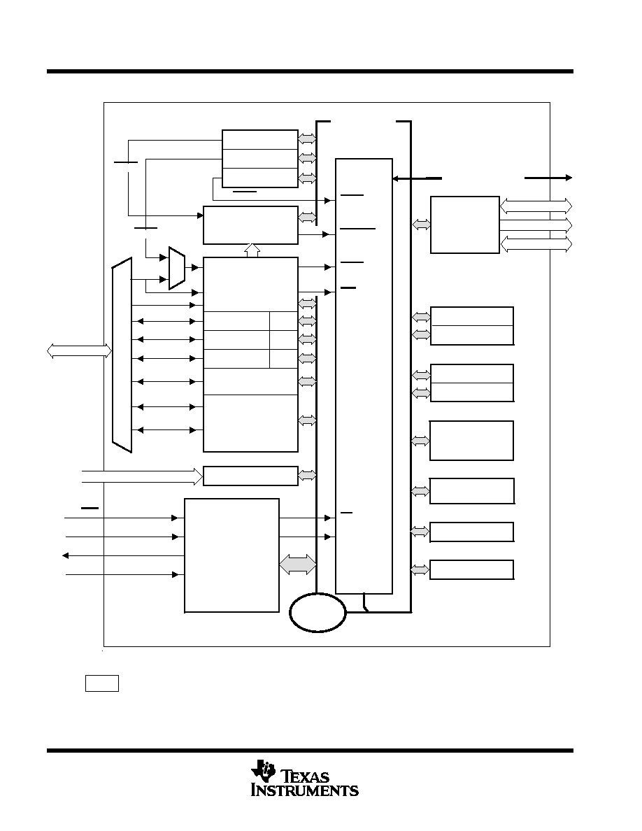
Functional Block Diagram
4
. . . . . . . . . . . . . . . . . . . . . . . .
Pin Functions
8
. . . . . . . . . . . . . . . . . . . . . . . . . . . . . . . . . . .
Memory Map
12
. . . . . . . . . . . . . . . . . . . . . . . . . . . . . . . . . .
Description
16
. . . . . . . . . . . . . . . . . . . . . . . . . . . . . . . . . . . .
C28x CPU
16
. . . . . . . . . . . . . . . . . . . . . . . . . . . . . . . . . . .
Memory Bus (Harvard Bus Architecture)
16
. . . . . . . . .
Peripheral Bus
16
. . . . . . . . . . . . . . . . . . . . . . . . . . . . . . . .
Real-Time JTAG and Analysis
17
. . . . . . . . . . . . . . . . . .
External Interface (XINTF) (F2812 Only)
17
. . . . . . . . .
Flash
17
. . . . . . . . . . . . . . . . . . . . . . . . . . . . . . . . . . . . . . . .
M0, M1 SARAMs
17
. . . . . . . . . . . . . . . . . . . . . . . . . . . . .
L0, L1, H0 SARAMs
17
. . . . . . . . . . . . . . . . . . . . . . . . . . .
Boot ROM
17
. . . . . . . . . . . . . . . . . . . . . . . . . . . . . . . . . . .
Security
18
. . . . . . . . . . . . . . . . . . . . . . . . . . . . . . . . . . . . . .
Peripheral Interrupt Expansion (PIE) Block
19
. . . . . . .
External Interrupts (XINT1, 2, 13, XNMI)
19
. . . . . . . . .
Oscillator and PLL
19
. . . . . . . . . . . . . . . . . . . . . . . . . . . .
Watchdog
19
. . . . . . . . . . . . . . . . . . . . . . . . . . . . . . . . . . . .
Peripheral Clocking
19
. . . . . . . . . . . . . . . . . . . . . . . . . . . .
Low-Power Modes
19
. . . . . . . . . . . . . . . . . . . . . . . . . . . .
Peripheral Frames 0, 1, 2 (PFn)
20
. . . . . . . . . . . . . . . . .
General-Purpose Input/Output (GPIO) Multiplexer
20
.
32-Bit CPU-Timers (0, 1, 2)
20
. . . . . . . . . . . . . . . . . . . . .
Motor Control Peripherals
20
. . . . . . . . . . . . . . . . . . . . . .
Serial Port Peripherals
21
. . . . . . . . . . . . . . . . . . . . . . . . .
Register Map
21
. . . . . . . . . . . . . . . . . . . . . . . . . . . . . . . . . .
Device Emulation Registers
24
. . . . . . . . . . . . . . . . . . . . . .
External Interface, XINTF (F2812 only)
27
. . . . . . . . . . . .
Interrupts
34
. . . . . . . . . . . . . . . . . . . . . . . . . . . . . . . . . . . . . .
Vector Table Mapping
36
. . . . . . . . . . . . . . . . . . . . . . . . . .
PIE Vector Map
38
. . . . . . . . . . . . . . . . . . . . . . . . . . . . . . .
PIE Registers
39
. . . . . . . . . . . . . . . . . . . . . . . . . . . . . . . . .
PIE/CPU Interrupt Response
41
. . . . . . . . . . . . . . . . . . .
External Interrupts
42
. . . . . . . . . . . . . . . . . . . . . . . . . . . .
System Control
44
. . . . . . . . . . . . . . . . . . . . . . . . . . . . . . . .
OSC and PLL Block
49
. . . . . . . . . . . . . . . . . . . . . . . . . . . .
PLL-Based Clock Module
50
. . . . . . . . . . . . . . . . . . . . . . . .
External Reference Oscillator Clock Option
50
. . . . . . . .
Watchdog Block
51
. . . . . . . . . . . . . . . . . . . . . . . . . . . . . . . .
Low-Power Modes Block
54
. . . . . . . . . . . . . . . . . . . . . . . .
Peripherals
56
. . . . . . . . . . . . . . . . . . . . . . . . . . . . . . . . . . . .
32-Bit CPU-Timers 0/1/2
56
. . . . . . . . . . . . . . . . . . . . . . . .
Event Manager Modules (EVA, EVB)
61
. . . . . . . . . . . . . .
Enhanced Analog-to-Digital Converter
(ADC) Module
67
. . . . . . . . . . . . . . . . . . . . . . . . . . . . .
Enhanced Controller Area Network (eCAN) Module
71
.
Multichannel Buffered Serial Port (McBSP) Module
75
. .
Serial Communications Interface (SCI) Module
79
. . . . .
Serial Peripheral Interface (SPI) Module
82
. . . . . . . . . . .
GPIO Mux
85
. . . . . . . . . . . . . . . . . . . . . . . . . . . . . . . . . . . . .
Development Support
95
. . . . . . . . . . . . . . . . . . . . . . . . . . .
Documentation Support
97
. . . . . . . . . . . . . . . . . . . . . . . . .
Absolute Maximum Ratings
98
. . . . . . . . . . . . . . . . . . . . . .
Recommended Operating Conditions
98
. . . . . . . . . . . . .
Electrical Characteristics Over Recommended
Operating Free-Air Temperature Range
99
. . . . . . . .
Mechanical Data
100
. . . . . . . . . . . . . . . . . . . . . . . . . . . . . .
Table of Contents
PR
O
DU
C
T PREVIEW
TMS320F2810, TMS320F2812
DIGITAL SIGNAL PROCESSORS
SPRS174B Ł APRIL 2001 Ł REVISED SEPTEMBER 2001
3
POST OFFICE BOX 1443
Ę
HOUSTON, TEXAS 77251Ł1443
device summary
Note that throughout this data sheet, F2810 is used to denote TMS320F2810; F2812 is used to denote
TMS320F2812; and F28x is used to denote F2810 and F2812.
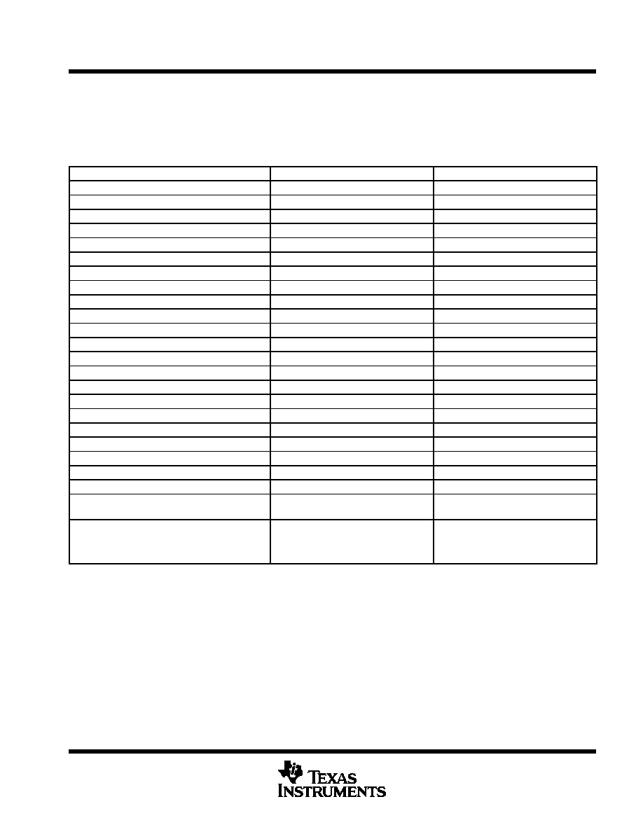
Table 1. Hardware Features of the F2810 and F2812 Devices
FEATURE
F2810
F2812
Instruction Cycle (at 150 MHz)
6.67 ns
6.67 ns
Single-Access RAM (SARAM) (16-bit word)
18K
18K
3.3-V On-Chip Flash (16-bit word)
64K
128K
Code Security for On-Chip Flash/SARAM
Yes
Yes
Boot ROM
Yes
Yes
OTP ROM
Yes
Yes
External Memory Interface
--
Yes
Event Managers A and B (EVA and EVB)
EVA, EVB
EVA, EVB
S
General-Purpose (GP) Timers
4
4
S
Compare (CMP)/PWM
16
16
S
Capture (CAP)/QEP Channels
6/2
6/2
Watchdog Timer
Yes
Yes
12-Bit ADC
Yes
Yes
S
Channels
16
16
32-bit CPU Timers
3
3
SPI
Yes
Yes
SCIA, SCIB
SCIA, SCIB
SCIA, SCIB
CAN
Yes
Yes
McBSP
Yes
Yes
Digital I/O Pins (Shared)
56
56
External Interrupts
3
3
Supply Voltage
1.8-V Core, 3.3-V I/O
1.8-V Core, 3.3-V I/O
Packaging
128-pin PBK
179-pin GHH
176-pin PGF
Product Status:
Product Preview (PP)
Advance Information (AI)
Production Data (PD)
PP
PP
PR
O
DU
C
T PREVIEW