TMS320C6712, TMS320C6712C Floating-Point Digital Signal Processors (Rev. D)
TMS320C6712, TMS320C6712C
FLOATING POINT DIGITAL SIGNAL PROCESSORS
SPRS148D AUGUST 2000 REVISED MARCH 2003
1
POST OFFICE BOX 1443
·
HOUSTON, TEXAS 772511443
D
Best Price/Performance Digital Signal
Processors (DSPs): TMS320C67x
(TMS320C6712, TMS320C6712C)
Eight 32-Bit Instructions/Cycle
100-, 150-MHz Clock Rates
10-, 6.7-ns Instruction Cycle Times
600, 900 MFLOPS
D
VelociTI
Advanced Very Long Instruction
Word (VLIW) C67x
DSP Core
Eight Highly Independent Functional
Units:
Four ALUs (Floating- and Fixed-Point)
Two ALUs (Fixed-Point)
Two Multipliers (Floating- and
Fixed-Point)
Load-Store Architecture With 32 32-Bit
General-Purpose Registers
Instruction Packing Reduces Code Size
All Instructions Conditional
D
Instruction Set Features
Hardware Support for IEEE
Single-Precision and Double-Precision
Instructions
Byte-Addressable (8-, 16-, 32-Bit Data)
8-Bit Overflow Protection
Saturation
Bit-Field Extract, Set, Clear
Bit-Counting
Normalization
D
L1/L2 Memory Architecture
32K-Bit (4K-Byte) L1P Program Cache
(Direct Mapped)
32K-Bit (4K-Byte) L1D Data Cache
(2-Way Set-Associative)
512K-Bit (64K-Byte) L2 Unified Mapped
RAM/Cache
(Flexible Data/Program Allocation)
D
Device Configuration
Boot Mode: 8- and 16-Bit ROM Boot
Endianness: Little Endian
D
Enhanced Direct-Memory-Access (EDMA)
Controller (16 Independent Channels)
D
16-Bit External Memory Interface (EMIF)
Glueless Interface to Asynchronous
Memories: SRAM and EPROM
Glueless Interface to Synchronous
Memories: SDRAM and SBSRAM
256M-Byte Total Addressable External
Memory Space
D
Two Multichannel Buffered Serial Ports
(McBSPs)
Direct Interface to T1/E1, MVIP, SCSA
Framers
ST-Bus-Switching Compatible
Up to 256 Channels Each
AC97-Compatible
Serial-Peripheral-Interface (SPI)
Compatible (Motorola
)
D
Two 32-Bit General-Purpose Timers
D
Flexible Phase-Locked-Loop (PLL) Clock
Generator [C6712]
D
Flexible Software-Configurable PLL-Based
Clock Generator Module [C6712C]
D
A Dedicated General-Purpose Input/Output
(GPIO) Module With 5 Pins [C6712C]
D
IEEE-1149.1 (JTAG
)
Boundary-Scan-Compatible
D
256-Pin Ball Grid Array (BGA) Package
(GFN Suffix) [C6712 Only]
D
272-Pin Ball Grid Array (BGA) Package
(GDP Suffix) [C6712C Only]
D
CMOS Technology
0.13-
µ
m/6-Level Copper Metal Process
(C6712C)
0.18-
µ
m/5-Level Metal Process (C6712)
D
3.3-V I/Os, 1.26-V Internal (C6712C)
D
3.3-V I/Os, 1.8-V Internal (C6712)
Please be aware that an important notice concerning availability, standard warranty, and use in critical applications of
Texas Instruments semiconductor products and disclaimers thereto appears at the end of this data sheet.
Copyright
2003, Texas Instruments Incorporated
TMS320C67x, VelociTI, and C67x are trademarks of Texas Instruments.
Motorola is a trademark of Motorola, Inc.
Other trademarks are the property of their respective owners.
IEEE Standard 1149.1-1990 Standard-Test-Access Port and Boundary Scan Architecture.
PRODUCTION DATA information is current as of publication date.
Products conform to specifications per the terms of Texas Instruments
standard warranty. Production processing does not necessarily include
testing of all parameters.
TMS320C6712, TMS320C6712C
FLOATING POINT DIGITAL SIGNAL PROCESSORS
SPRS148D AUGUST 2000 REVISED MARCH 2003
2
POST OFFICE BOX 1443
·
HOUSTON, TEXAS 772511443
Table of Contents
bootmode
54
. . . . . . . . . . . . . . . . . . . . . . . . . . . . . . . . . . . . . .
absolute maximum ratings over operating case
temperature range
55
. . . . . . . . . . . . . . . . . . . . . . . . . .
recommended operating conditions
55
. . . . . . . . . . . . . . . .
electrical characteristics over recommended ranges of
supply voltage and operating case temperature
56
.
parameter measurement information
57
. . . . . . . . . . . . . . .
signal transition levels
58
. . . . . . . . . . . . . . . . . . . . . . . . . .
timing parameters and board routing analysis
58
. . . . . .
input and output clocks
60
. . . . . . . . . . . . . . . . . . . . . . . . . . .
asynchronous memory timing
65
. . . . . . . . . . . . . . . . . . . . .
synchronous-burst memory timing
68
. . . . . . . . . . . . . . . . .
synchronous DRAM timing
70
. . . . . . . . . . . . . . . . . . . . . . . .
HOLD/HOLDA timing
76
. . . . . . . . . . . . . . . . . . . . . . . . . . . .
BUSREQ timing
77
. . . . . . . . . . . . . . . . . . . . . . . . . . . . . . . . .
reset timing [C6712]
78
. . . . . . . . . . . . . . . . . . . . . . . . . . . . .
reset timing [C6712C]
80
. . . . . . . . . . . . . . . . . . . . . . . . . . . .
external interrupt timing
82
. . . . . . . . . . . . . . . . . . . . . . . . . .
multichannel buffered serial port timing
83
. . . . . . . . . . . . .
timer timing
97
. . . . . . . . . . . . . . . . . . . . . . . . . . . . . . . . . . . . .
general-purpose input/output (GPIO) port timing
[C6712C only]
98
. . . . . . . . . . . . . . . . . . . . . . . . . . . . . .
JTAG test-port timing
99
. . . . . . . . . . . . . . . . . . . . . . . . . . . .
mechanical data [C6712 only]
100
. . . . . . . . . . . . . . . . . . . .
mechanical data [C6712C only]
101
. . . . . . . . . . . . . . . . . .
revision history
102
. . . . . . . . . . . . . . . . . . . . . . . . . . . . . . . . .
GFN BGA package (bottom view) [C6712 only]
3
. . . . . . . . . .
GDP BGA package (bottom view) [C6712C only]
3
. . . . . . . .
description
4
. . . . . . . . . . . . . . . . . . . . . . . . . . . . . . . . . . . . . . . . .
device characteristics
5
. . . . . . . . . . . . . . . . . . . . . . . . . . . . . . . .
device compatibility
6
. . . . . . . . . . . . . . . . . . . . . . . . . . . . . . . . . .
functional block and CPU (DSP core) diagram
7
. . . . . . . . . . .
CPU (DSP core) description
8
. . . . . . . . . . . . . . . . . . . . . . . . . .
memory map summary
10
. . . . . . . . . . . . . . . . . . . . . . . . . . . . . .
peripheral register descriptions
11
. . . . . . . . . . . . . . . . . . . . . . .
signal groups description
16
. . . . . . . . . . . . . . . . . . . . . . . . . . . .
device configurations
18
. . . . . . . . . . . . . . . . . . . . . . . . . . . . . . .
terminal functions
21
. . . . . . . . . . . . . . . . . . . . . . . . . . . . . . . . . .
development support
32
. . . . . . . . . . . . . . . . . . . . . . . . . . . . . . . .
documentation support
35
. . . . . . . . . . . . . . . . . . . . . . . . . . . . . .
CPU CSR register description
36
. . . . . . . . . . . . . . . . . . . . . . . .
interrupt sources and interrupt selector [C6712 only]
38
. . . .
interrupt sources and interrupt selector [C6712C only]
39
. . .
EDMA channel synchronization events [C6712 only]
40
. . . .
EDMA module and EDMA selector [C6712C only]
41
. . . . . . .
clock PLL [C6712 only]
43
. . . . . . . . . . . . . . . . . . . . . . . . . . . . . .
PLL and PLL controller [C6712C only]
45
. . . . . . . . . . . . . . . . .
power-supply sequencing
52
. . . . . . . . . . . . . . . . . . . . . . . . . . . .
power-supply decoupling
53
. . . . . . . . . . . . . . . . . . . . . . . . . . . .
IEEE 1149.1 JTAG compatibility statement
53
. . . . . . . . . . . . .
EMIF device speed
54
. . . . . . . . . . . . . . . . . . . . . . . . . . . . . . . . .
TMS320C6712, TMS320C6712C
FLOATING POINT DIGITAL SIGNAL PROCESSORS
SPRS148D AUGUST 2000 REVISED MARCH 2003
3
POST OFFICE BOX 1443
·
HOUSTON, TEXAS 772511443
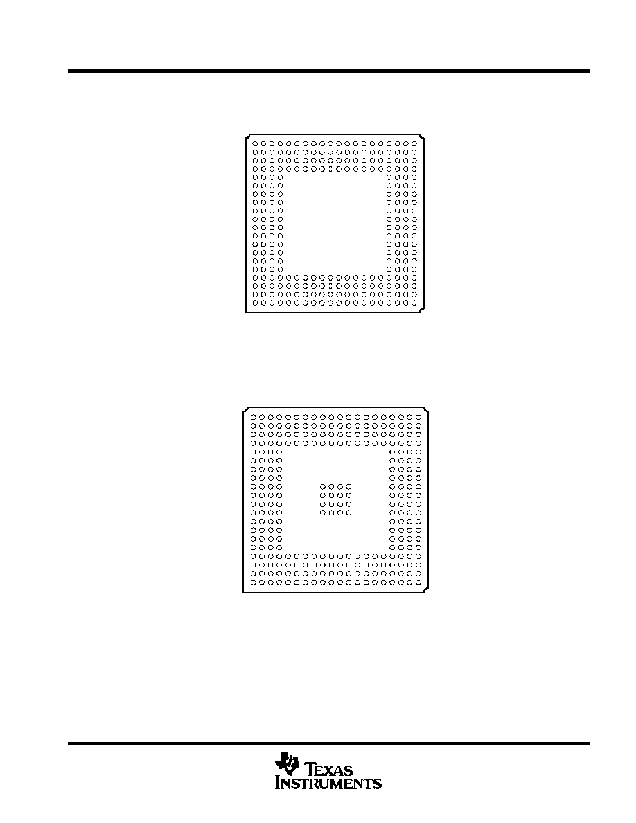
GFN BGA package (bottom view) [C6712 only]
19
15
17
13
11
9
Y
V
T
U
P
N
R
W
7
5
L
J
K
H
F
G
3
1
D
B
C
A
E
M
2
4
6
8
20
18
16
14
12
10
GFN 256-PIN BALL GRID ARRAY (BGA) PACKAGE
(BOTTOM VIEW)
GDP BGA package (bottom view) [C6712C only]
GDP 272-PIN BALL GRID ARRAY (BGA) PACKAGE
(BOTTOM VIEW)
2
4
6
8
20
18
16
14
12
10
M
E
A
1
C
B
D
G
F
H
K
J
L
W
R
N
P
U
T
V
Y
3
5
7
9
11
17
15
13
19

TMS320C6712, TMS320C6712C
FLOATING POINT DIGITAL SIGNAL PROCESSORS
SPRS148D AUGUST 2000 REVISED MARCH 2003
4
POST OFFICE BOX 1443
·
HOUSTON, TEXAS 772511443
description
The TMS320C67x
DSPs (including the TMS320C6712, TMS320C6712C devices
) are members of the
floating-point DSP family in the TMS320C6000
DSP platform. The C6712 and C6712C devices are based on
the high-performance, advanced VelociTI
very-long-instruction-word (VLIW) architecture developed by Texas
Instruments (TI), making these DSPs an excellent choice for multichannel and multifunction applications.
With performance of up to 900 million floating-point operations per second (MFLOPS) at a clock rate of
150 MHz, the C6712C device is the lowest-cost DSP in the C6000
DSP platform. The C6712C DSP
possesses the operational flexibility of high-speed controllers and the numerical capability of array processors.
This processor has 32 general-purpose registers of 32-bit word length and eight highly independent functional
units. The eight functional units provide four floating-/fixed-point ALUs, two fixed-point ALUs, and two
floating-/fixed-point multipliers. The C6712C can produce two MACs per cycle for a total of 300 MMACS.
With performance of up to 600 million floating-point operations per second (MFLOPS) at a clock rate of
100 MHz, the C6712 device also offers cost-effective solutions to high-performance DSP programming
challenges. The C6712 DSP possesses the operational flexibility of high-speed controllers and the numerical
capability of array processors. This processor has 32 general-purpose registers of 32-bit word length and eight
highly independent functional units. The eight functional units provide four floating-/fixed-point ALUs, two
fixed-point ALUs, and two floating-/fixed-point multipliers. The C6712 can produce two multiply-accumulates
(MACs) per cycle for a total of 200 million MACs per second (MMACS).
The C6712/C6712C uses a two-level cache-based architecture and has a powerful and diverse set of
peripherals. The Level 1 program cache (L1P) is a 32-Kbit direct mapped cache and the Level 1 data cache
(L1D) is a 32-Kbit 2-way set-associative cache. The Level 2 memory/cache (L2) consists of a 512-Kbit memory
space that is shared between program and data space. L2 memory can be configured as mapped memory,
cache, or combinations of the two. The peripheral set includes two multichannel buffered serial ports (McBSPs),
two general-purpose timers, and a glueless 16-bit external memory interface (EMIF) capable of interfacing to
SDRAM, SBSRAM, and asynchronous peripherals. The C6712C device also includes a dedicated
general-purpose input/output (GPIO) peripheral module.
The C6712/C6712C DSPs also have application-specific hardware logic, on-chip memory, and additional
on-chip peripherals.
The C6712/C6712C has a complete set of development tools which includes: a new C compiler, an assembly
optimizer to simplify programming and scheduling, and a Windows
debugger interface for visibility into source
code execution.
TMS320C6000 and C6000 are trademarks of Texas Instruments.
Windows is a registered trademark of the Microsoft Corporation.
Throughout the remainder of this document, the TMS320C6712 and TMS320C6712C shall be referred to as TMS320C67x or C67x where
generic, and where specific, their individual full device part numbers will be used or abbreviated as C6712 or C6712C.
TMS320C6712, TMS320C6712C
FLOATING POINT DIGITAL SIGNAL PROCESSORS
SPRS148D AUGUST 2000 REVISED MARCH 2003
5
POST OFFICE BOX 1443
·
HOUSTON, TEXAS 772511443
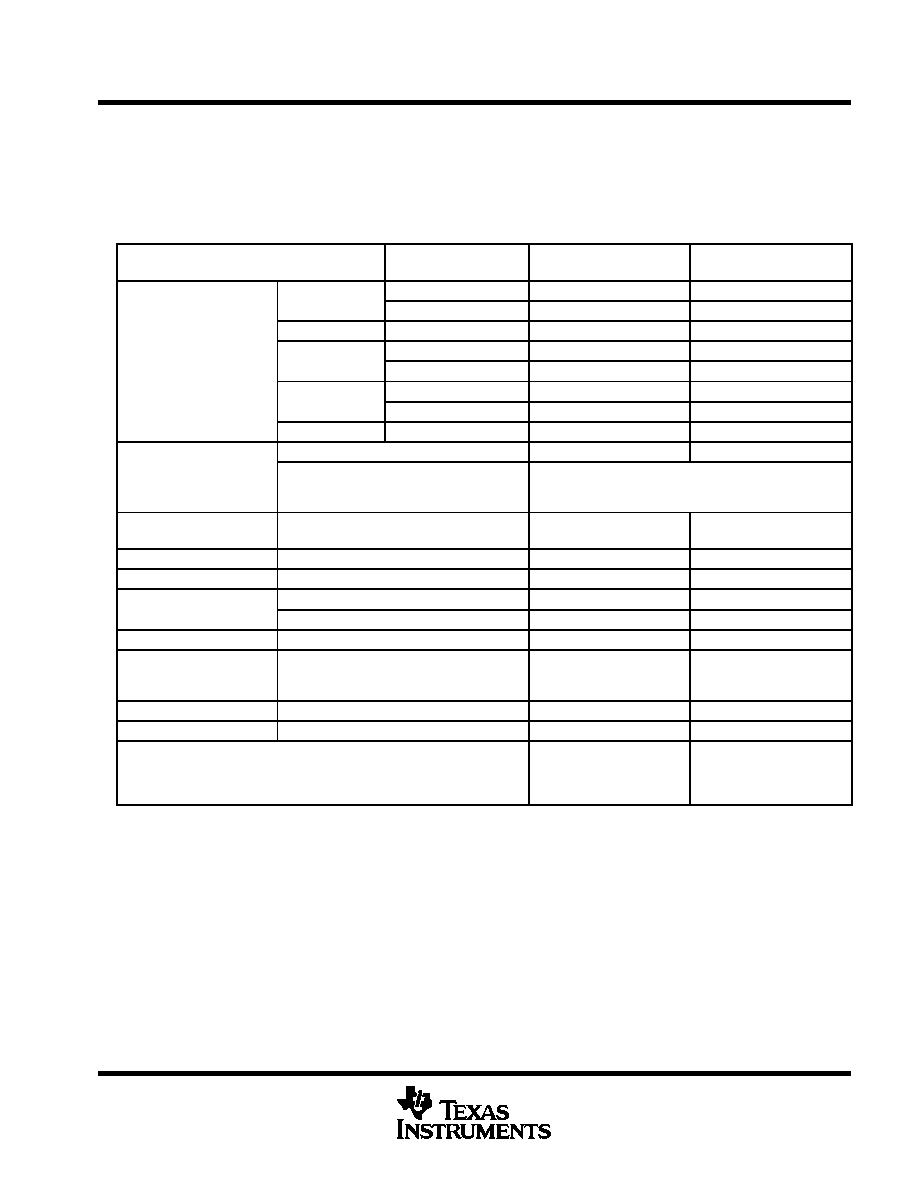
device characteristics
Table 1 provides an overview of the C6712/C6712C DSPs. The table shows significant features of each device,
including the capacity of on-chip RAM, the peripherals, the execution time, and the package type with pin count.
For more details on the C6000
DSP device part numbers and part numbering, see Table 17 and Figure 5.
Table 1. Characteristics of the C6712 and C6712C Processors
HARDWARE FEATURES
INTERNAL CLOCK
SOURCE
C6712
(FLOATING-POINT DSP)
C6712C
(FLOATING-POINT DSP)
EMIF
ECLKIN
1
EMIF
SYSCLK3 or ECLKIN
1
EDMA
CPU clock frequency
1
1
Peripherals
McBSPs
CPU/2 clock frequency
2
--
Peripherals
McBSPs
SYSCLK2
--
2
32 Bit Timers
CPU/4 clock frequency
2
--
32-Bit Timers
1/4 of SYSCLK1
--
2
GPIO Module
SYSCLK2
--
1
Size (Bytes)
72K
72K
On-Chip Memory
Organization
4K-Byte (4KB) L1 Program (L1P) Cache
4KB L1 Data (L1D) Cache
64KB Unified Mapped RAM/Cache (L2)
CPU ID+
CPU Rev ID
Control Status Register (CSR.[31:16])
0x0202
0x0203
Frequency
MHz
100
150
Cycle Time
ns
10 ns (C6712-100)
6.7 ns (C6712C-150)
Voltage
Core (V)
1.8
1.26
Voltage
I/O (V)
3.3
3.3
PLL Options
CLKIN frequency multiplier
Bypass (x1), x4
Clock Generator Options
Prescaler
Multiplier
Postscaler
--
/1, /2, /3, ..., /32
x4, x5, x6, ..., x25
/1, /2, /3, ..., /32
BGA Package
27 x 27 mm
256-Pin BGA (GFN)
272-Pin BGA (GDP)
Process Technology
µ
m
0.18
µ
m
0.13
µ
m
Product Status
Product Preview (PP)
Advance Information (AI)
Production Data (PD)
PD
PD
PRODUCT PREVIEW information concerns products in the formative or design phase of development. Characteristic data and other
specifications are design goals. Texas Instruments reserves the right to change or discontinue these products without notice.
ADVANCE INFORMATION concerns new products in the sampling or preproduction phase of development. Characteristic data and
other specifications are subject to change without notice.
PRODUCTION DATA information is current as of publication date. Products conform to specifications per the terms of Texas
Instruments standard warranty. Production processing does not necessarily include testing of all parameters.
Document Outline
- features
- Table of Contents
- GFN BGA package (bottom view) [C6712 only]
- GDP BGA package (bottom view) [C6712C only]
- description
- device characteristics
- device compatibility
- functional block and CPU (DSP core) diagram
- CPU (DSP core) description
- memory map summary
- peripheral register descriptions
- signal groups description
- DEVICE CONFIGURATIONS
- device configurations at device reset
- DEVCFG register description [C6712C only]
- TERMINAL FUNCTIONS
- development support
- Software Development Tools:
- Hardware Development Tools:
- device and development-support tool nomenclature
- documentation support
- CPU CSR register description
- interrupt sources and interrupt selector [C6712 only]
- interrupt sources and interrupt selector [C6712C only]
- EDMA channel synchronization events [C6712 only]
- EDMA module and EDMA selector [C6712C only]
- ESEL0 Register (0x01A0 FF00)
- ESEL1 Register (0x01A0 FF04)
- ESEL3 Register (0x01A0 FF0C)
- clock PLL [C6712 only]
- PLL and PLL controller [C6712C only]
- PLLCSR Register (0x01B7 C100)
- PLLM Register (0x01B7 C110)
- PLLDIV0, PLLDIV1, PLLDIV2, and PLLDIV3 Registers
- OSCDIV1 Register (0x01B7 C124)
- power-supply sequencing
- system-level design considerations
- power-supply design considerations
- C6712 device applicable only
- power-supply decoupling
- IEEE 1149.1 JTAG compatibility statement
- C6712C device applicable only
- C6712 device applicable only
- EMIF device speed
- C6712C device applicable only
- bootmode
- absolute maximum ratings over operating case temperature range (unless \
otherwise noted)
- recommended operating conditions
- electrical characteristics over recommended ranges of supply voltage and\
operating case
temperature (unless otherwise note
- PARAMETER MEASUREMENT INFORMATION
- signal transition levels
- timing parameters and board routing analysis
- INPUT AND OUTPUT CLOCKS
- timing requirements for CLKIN (see Figure 16) [C6712]
- timing requirements for CLKIN (see Figure 16) [C6712C]
- switching characteristics over recommended operating conditions for CLKO\
UT1 (see Figure 17) [C6712 only]
- switching characteristics over recommended operating conditions for CLKO\
UT2 (see Figure 18)
[C6712]
- switching characteristics over recommended operating conditions for CLKO\
UT2 (see Figure 18) [C6712C]
- switching characteristics over recommended operating conditions for CLKO\
UT3 (see Figure 19) [C6712C only]
- timing requirements for ECLKIN (see Figure 20)
- switching characteristics over recommended operating conditions for ECLK\
OUT (see Figure 21)
- ASYNCHRONOUS MEMORY TIMING
- timing requirements for asynchronous memory cycles (see Figure 22-Figur\
e 23)
- switching characteristics over recommended operating conditions for asyn\
chronous memory cycles (see Figure 22-Figure 23)
- SYNCHRONOUS-BURST MEMORY TIMING
- timing requirements for synchronous-burst SRAM cycles (see Figure 24)
- switching characteristics over recommended operating conditions for sync\
hronous-burst SRAM cycles (see Figure 24 and Figure 2
- SYNCHRONOUS DRAM TIMING
- timing requirements for synchronous DRAM cycles (see Figure 26)
- switching characteristics over recommended operating conditions for sync\
hronous DRAM cycles (see Figure 26-Figure 32)
- HOLD/HOLDA TIMING
- timing requirements for the HOLD\/ HOLDA\ cycles (see Figure 33)
- switching characteristics over recommended operating conditions for the \
HOLD\/HOLDA\ cycles (see Figure 33)
- BUSREQ TIMING
- switching characteristics over recommended operating conditions for the \
BUSREQ cycles (see Figure 34)
- RESET TIMING [C6712]
- timing requirements for reset (see Figure 35)
- switching characteristics over recommended operating conditions during r\
eset (see Figure 35)
- RESET TIMING [C6712C]
- timing requirements for reset (see Figure 36)
- switching characteristics over recommended operating conditions during r\
eset (see Figure 36)
- EXTERNAL INTERRUPT TIMING
- timing requirements for external interrupts (see Figure 37)
- MULTICHANNEL BUFFERED SERIAL PORT TIMING
- timing requirements for McBSP (see Figure 38) [C6712]
- timing requirements for McBSP (see Figure 38) [C6712C]
- switching characteristics over recommended operating conditions for McBS\
P (see Figure 38)
[C6712]
- switching characteristics over recommended operating conditions for McBS\
P (see Figure 38)
[C6712C]
- timing requirements for FSR when GSYNC = 1 (see Figure 39)
- timing requirements for McBSP as SPI master or slave: CLKSTP = 10b, CLKX\
P = 0 (see Figure 40)
[C6712]
- timing requirements for McBSP as SPI master or slave: CLKSTP = 10b, CLKX\
P = 0 (see Figure 40)
[C6712C]
- switching characteristics over recommended operating conditions for McBS\
P as SPI master or slave: CLKSTP = 10b, CLKXP = 0
- switching characteristics over recommended operating conditions for McBS\
P as SPI master or slave: CLKSTP = 10b, CLKXP = 0
- timing requirements for McBSP as SPI master or slave: CLKSTP = 11b, CLKX\
P = 0 (see Figure 41)
[C6712]
- timing requirements for McBSP as SPI master or slave: CLKSTP = 11b, CLKX\
P = 0 (see Figure 41)
[C6712C]
- switching characteristics over recommended operating conditions for McBS\
P as SPI master or slave: CLKSTP = 11b, CLKXP = 0
- switching characteristics over recommended operating conditions for McBS\
P as SPI master or slave: CLKSTP = 11b, CLKXP = 0
- timing requirements for McBSP as SPI master or slave: CLKSTP = 10b, CLKX\
P = 1 (see Figure 42)
[C6712]
- timing requirements for McBSP as SPI master or slave: CLKSTP = 10b, CLKX\
P = 1 (see Figure 42)
[C6712C]
- switching characteristics over recommended operating conditions for McBS\
P as SPI master or slave: CLKSTP = 10b, CLKXP = 1
- switching characteristics over recommended operating conditions for McBS\
P as SPI master or slave: CLKSTP = 10b, CLKXP = 1
- timing requirements for McBSP as SPI master or slave: CLKSTP = 11b, CLKX\
P = 1 (see Figure 43)
[C6712]
- timing requirements for McBSP as SPI master or slave: CLKSTP = 11b, CLKX\
P = 1 (see Figure 43)
[C6712C]
- switching characteristics over recommended operating conditions for McBS\
P as SPI master or slave: CLKSTP = 11b, CLKXP = 1
- switching characteristics over recommended operating conditions for McBS\
P as SPI master or slave: CLKSTP = 11b, CLKXP = 1
- TIMER TIMING
- timing requirements for timer inputs (see Figure 44)
- switching characteristics over recommended operating conditions for time\
r outputs (see Figure 44)
- GENERAL-PURPOSE INPUT/OUTPUT (GPIO) PORT TIMING [C6712C ONLY]
- timing requirements for GPIO inputs (see Figure 45)
- switching characteristics over recommended operating conditions for GPIO\
outputs (see Figure 45)
- JTAG TEST-PORT TIMING
- timing requirements for JTAG test port (see Figure 46)
- switching characteristics over recommended operating conditions for JTAG\
test port (see Figure 46)
- MECHANICAL DATA [C6712 ONLY]
- GFN (S-PBGA-N256) [C6712 only] PLASTIC BALL GRID ARRAY
- thermal resistance characteristics (S-PBGA package) [C6712 only]
- MECHANICAL DATA [C6712C ONLY]
- GDP (S
PBGA
N272) [C6712C only] PLASTIC BALL GRID ARRAY
- thermal resistance characteristics (S-PBGA package) [C6712C only]
- REVISION HISTORY
- IMPORTANT NOTICE