Document Outline
- tms320C40 DIGITAL SIGNAL PROCESSOR
- features
- block diagram
- functions
- GF Package Pin Assignments ä Alphabetical Listing
- GF Package Pin Assignments ä Numerical Listing
- memory map
- description
- operation
- central processing unit
- DMA coprocessor
- communication ports
- communication-port software reset (ÉC40 silicon revision 5.0)
- IDLE2 clock-stop power-down mode (ÉC40 silicon revision
- development tools
- silicon revision identification
- absolute maximum ratings over specified temperature range (unless otherwise noted)ü
- recommended operating conditions (see Note 2)
- electrical characteristics over recommended ranges of supply voltage and operating case temperature ( unless otherwise noted)
- PARAMETER MEASUREMENT INFORMATION
- signal transition levels
- timing parameter symbology
- timing for IIOFx interrupt response [P =tc(H)] (see Notes 6, 7 and Figure 20)
- timing for IACK\ (see Note 9 anf Figure 21)
- communication-port word-transfer-cycle timingü [P = tc(H)] )see Note 10 and Figure 22)
- timing for communication-token transfer sequence, input to an output port [P =
- communication-port byte-cycle timing (write and read) (see Note 11 and Figure 23)
- timing for communication-token transfer sequence, input to an output port [P = tc(H)] (see Figure 24)ü
- timing for communication-token transfer sequence, output to an input port [P = tc(H)] (see Figure25)ü
- timer pin timing (see Note 12 and Figure 26)
- timing for IEEE-1149.1 test access port (see Figure 27)
- MECHANICAL DATA
- GF (S-CPGA-P325) CERAMIC PIN GRID ARRAY PACKAGE
- IMPORTANT NOTICE
See Pin Assignments table and Pin Functions table for location
and description of all pins.
1
2
3
4
5
6
7
8
9
10
11 13
12
15
14 16
17
18
19
20
21
22
23
24
25
26 28
27
30
29 31
32
33
34
35
A
B
C
D
E
F
G
H
J
K
L
M
N
P
R
T
U
V
W
Y
AA
AB
AC
AD
AE
AF
AG
AH
AJ
AK
AL
AM
AN
AP
AR
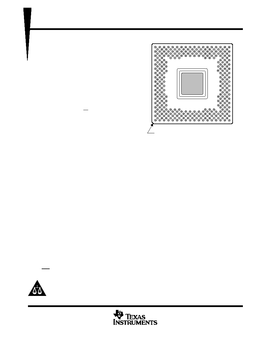
Pin A1
325-PIN GF GRID ARRAY PACKAGE
(BOTTOM VIEW)
x
TMS320C40
DIGITAL SIGNAL PROCESSOR
SPRS038 Ł JANUARY 1996
1
POST OFFICE BOX 1443
Ę
HOUSTON, TEXAS 77251Ł1443
D
Highest Performance Floating-Point Digital
Signal Processor (DSP)
Ł '320C40-60:
33-ns Instruction Cycle Time,
330 MOPS, 60 MFLOPS,
30 MIPS, 384M Bytes / s
Ł '320C40-50:
40-ns Instruction Cycle Time
Ł '320C40-40:
50-ns Instruction Cycle Time
D
Six Communications Ports
D
Six-Channel Direct Memory Access (DMA)
Coprocessor
D
Single-Cycle Conversion to and From
IEEE-754 Floating-Point Format
D
Single Cycle, 1/x, 1/
D
Source-Code Compatible With TMS320C3x
D
Single-Cycle 40-Bit Floating-Point,
32-Bit Integer Multipliers
D
Twelve 40-Bit Registers, Eight Auxiliary
Registers, 14 Control Registers, and Two
Timers
D
IEEE 1149.1
(JTAG) Boundary Scan
Compatible
D
Two Identical External Data and Address
Buses Supporting Shared Memory Systems
and High Data-Rate, Single-Cycle
Transfers:
Ł High Port-Data Rate of 120M Bytes/s
('C40-60) (Each Bus)
Ł 16G-Byte Continuous
Program/ Data / Peripheral Address
Space
Ł Memory-Access Request for Fast,
Intelligent Bus Arbitration
Ł Separate Address-Bus, Data-Bus, and
Control-Enable Pins
Ł Four Sets of Memory-Control Signals
Support Different Speed Memories in
Hardware
D
325-Pin Ceramic Grid Array (GF Suffix)
D
Fabricated Using 0.72-
Ą
m Enhanced
Performance Implanted CMOS (EPIC
TM
)
Technology by Texas Instruments (TI
TM
)
D
Software-Communication-Port Reset
D
NMI With Bus-Grant Feature
D
Separate Internal Program, Data, and DMA
Coprocessor Buses for Support of Massive
Concurrent Input / Output (I/O) of Program
and Data Throughput, Maximizing
Sustained Central Processing Unit (CPU)
Performance
D
On-Chip Program Cache and
Dual-Access/Single-Cycle RAM for
Increased Memory-Access Performance
Ł 512-Byte Instruction Cache
Ł 8K Bytes of Single-Cycle Dual-Access
Program or Data RAM
Ł ROM-Based Boot Loader Supports
Program Bootup Using 8-, 16-, or 32-Bit
Memories or One of the Communication
Ports
D
IDLE2 Clock-Stop Power-Down Mode
D
5-V Operation
Please be aware that an important notice concerning availability, standard warranty, and use in critical applications of
Texas Instruments semiconductor products and disclaimers thereto appears at the end of this data sheet.
PRODUCTION DATA information is current as of publication date.
Products conform to specifications per the terms of Texas Instruments
standard warranty. Production processing does not necessarily include
testing of all parameters.
Copyright
®
1996, Texas Instruments Incorporated
IEEE Standard 1149.1Ł1990 Standard Test-Access Port and Boundary-Scan Architecture
EPIC and TI are trademarks of Texas Instruments Incorporated.
TMS320C40
DIGITAL SIGNAL PROCESSOR
SPRS038 Ł JANUARY 1996
2
POST OFFICE BOX 1443
Ę
HOUSTON, TEXAS 77251Ł1443
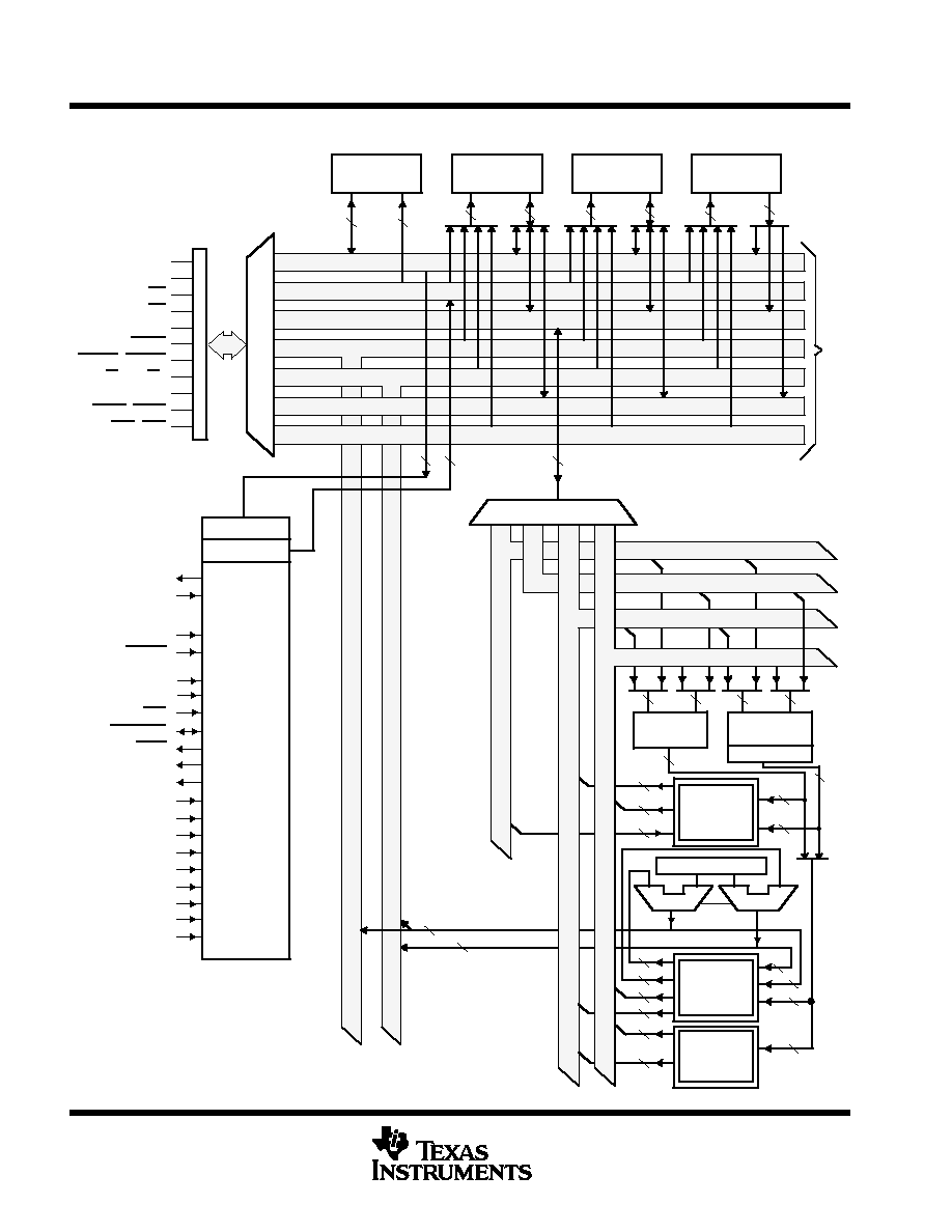
block diagram
Cache
(512 Bytes)
32
32
PDATA Bus
DDATA Bus
DADDR 1 Bus
DADDR 2 Bus
DMADATA Bus
RAM Block 0
(4K Bytes)
32
32
RAM Block 1
(4K Bytes)
32
32
ROM Block
(Reserved)
32
32
PADDR Bus
DMAADDR Bus
M
U
X
D(31Ł0)
A(30Ł0)
DE
AE
STAT(3 Ł 0)
LOCK
STRB0, STRB1
R / W0, R / W1
PAGE0, PAGE1
RDY0, RDY1
CE0, CE1
IR
PC
X1
X2/CLKIN
ROMEN
RESET
RESETLOC0
RESETLOC1
NMI
IIOF(3 Ł 0)
IACK
H1
H3
CVSS
DVDD
DVSS
IVSS
LADVDD
LDDVDD
VDDL
VSSL
SUBS
32
32
40
40
40
40
32-Bit Barrel
Shifter
40
40
ALU
Extended
Precision
Registers
(R0ŁR11)
40
40
32
40
40
DISP, IR0, IR1
ARAU0
ARAU1
BK
Auxiliary
Registers
(AR0ŁAR7)
Other
Registers
(14)
CPU1
CPU2
32
32
32
32
32
32
32
32
32
32
REG1
REG2
32
MUX
C
P
U
1
R
E
G
2
Multiplier
Continued on next page
32
32
Controller
R
E
G
1

TMS320C40
DIGITAL SIGNAL PROCESSOR
SPRS038 Ł JANUARY 1996
3
POST OFFICE BOX 1443
Ę
HOUSTON, TEXAS 77251Ł1443
block diagram (continued)
LD31 Ł LD0
LA30 Ł LA0
LDE
LAE
LSTAT3 Ł LSTAT0
LLOCK
LSTRB0 Ł LSTRB1
LR / W0 Ł LR / W1
LPAGE0 Ł LPAGE1
LRDY0 Ł LRDY1
LCE0,LCE1
DMA Channel 0
DMA Channel 1
DMA Channel 2
DMA Channel 3
DMA Channel 4
DMA Channel 5
DMA Coprocessor
Six DMA Channels
32
32
Global
Local
Port Control
Global-Control Register
Time-Period Register
Timer 1
Timer-Counter Register
TCLK1
Global-Control Register
Time-Period Register
Timer 0
Timer-Counter Register
TCLK0
Port-Control Registers
Output
FIFO
Input
FIFO
PAU
COM Port 0
CREQ0
CACK0
CSTRB0
CRDY0
C0D7ŁC0D0
Continued from previous page
Port-Control Registers
Output
FIFO
Input
FIFO
PAU
COM Port 5
CREQ5
CACK5
CSTRB5
CRDY5
C5D7Ł C5D0
MUX
DDATA Bus
DADDR 1 Bus
DADDR 2 Bus
DMADATA Bus
PADDR Bus
DMAADDR Bus
PDATA Bus
M
U
X
Six Communication Ports
Peripheral Data Bus
Peripheral Address
Bus
TMS320C40
DIGITAL SIGNAL PROCESSOR
SPRS038 Ł JANUARY 1996
4
POST OFFICE BOX 1443
Ę
HOUSTON, TEXAS 77251Ł1443
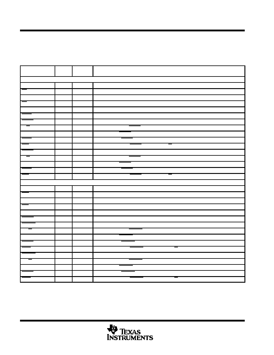
functions
This section lists signal descriptions for the '320C40 device. The '320C40 pin functions table lists each signal,
number of pins, operating mode(s) (that is, input, output, or high-impedance state as indicated by I, O, or Z,
respectively ), and function. The signals are grouped according to function.
Pin Functions
NAME
NO. OF
PINS
TYPE
DESCRIPTION
GLOBAL-BUS EXTERNAL INTERFACE ( 80 PINS)
D31 Ł D0
32
I / O / Z
32-bit data port of the global-bus external interface
DE
1
I
Data-bus-enable signal for the global-bus external interface
A30 Ł A0
31
O / Z
31-bit address port of the global-bus external interface
AE
1
I
Address-bus-enable signal for the global-bus external interface
STAT3 Ł STAT0
4
O
Status signals for the global-bus external interface
LOCK
1
O
Lock signal for the global-bus external interface
STRB0
1
O / Z
Access strobe 0 for the global-bus external interface
R / W0
1
O / Z
Read / write signal for STRB0 accesses
PAGE0
1
O / Z
Page signal for STRB0 accesses
RDY0
1
I
Ready signal for STRB0 accesses
CE0
1
I
Control enable for the STRB0, PAGE0, and R / W0 signals
STRB1
1
O / Z
Access strobe 1 for the global-bus external interface
R / W1
1
O / Z
Read / write signal for STRB1 accesses
PAGE1
1
O / Z
Page signal for STRB1 accesses
RDY1
1
I
Ready signal for STRB1 accesses
CE1
1
I
Control enable for the STRB1, PAGE1, and R / W1 signals
LOCAL-BUS EXTERNAL INTERFACE ( 80 PINS)
LD31 Ł LD0
32
I / O / Z
32-bit data port of the local-bus external interface
LDE
1
I
Data-bus-enable signal for the local-bus external interface
LA30 Ł LA0
31
O / Z
31-bit address port of the local-bus external interface
LAE
1
I
Address-bus-enable signal for the local-bus external interface
LSTAT3 Ł LSTAT0
4
O
Status signals for the local-bus external interface
LLOCK
1
O
Lock signal for the local-bus external interface
LSTRB0
1
O / Z
Access strobe 0 for the local-bus external interface
LR / W0
1
O / Z
Read / write signal for LSTRB0 accesses
LPAGE0
1
O / Z
Page signal for LSTRB0 accesses
LRDY0
1
I
Ready signal for LSTRB0 accesses
LCE0
1
I
Control enable for the LSTRB0, LPAGE0, and LR / W0 signals
LSTRB1
1
O / Z
Access strobe 1 for the local-bus external interface
LR / W1
1
O / Z
Read / write signal for LSTRB1 accesses
LPAGE1
1
O / Z
Page signal for LSTRB1 accesses
LRDY1
1
I
Ready signal for LSTRB1 accesses
LCE1
1
I
Control enable for the LSTRB1, LPAGE1, and LR / W1 signals
I = input, O = output, Z = high impedance
Signal's effective address range is defined by the local / global STRB ACTIVE bits.

TMS320C40
DIGITAL SIGNAL PROCESSOR
SPRS038 Ł JANUARY 1996
5
POST OFFICE BOX 1443
Ę
HOUSTON, TEXAS 77251Ł1443
Pin Functions ( Continued)
NAME
NO. OF
PINS
TYPE
DESCRIPTION
COMMUNICATION PORT 0 INTERFACE ( 12 PINS)
C0D7 Ł C0D0
8
I / O
Communication port 0 data bus
CREQ0
1
I / O
Communication port 0 token-request signal
CACK0
1
I / O
Communication port 0 token-request-acknowledge signal
CSTRB0
1
I / O
Communication port 0 data-strobe signal
CRDY0
1
I / O
Communication port 0 data-ready signal
COMMUNICATION PORT 1 INTERFACE ( 12 PINS)
C1D7 Ł C1D0
8
I / O
Communication port 1 data bus
CREQ1
1
I / O
Communication port 1 token-request signal
CACK1
1
I / O
Communication port 1 token-request-acknowledge signal
CSTRB1
1
I / O
Communication port 1 data-strobe signal
CRDY1
1
I / O
Communication port 1 data-ready signal
COMMUNICATION PORT 2 INTERFACE ( 12 PINS)
C2D7 Ł C2D0
8
I / O
Communication port 2 data bus
CREQ2
1
I / O
Communication port 2 token-request signal
CACK2
1
I / O
Communication port 2 token-request-acknowledge signal
CSTRB2
1
I / O
Communication port 2 data-strobe signal
CRDY2
1
I / O
Communication port 2 data-ready signal
COMMUNICATION PORT 3 INTERFACE ( 12 PINS)
C3D7 Ł C3D0
8
I / O
Communication port 3 data bus
CREQ3
1
I / O
Communication port 3 token-request signal
CACK3
1
I / O
Communication port 3 token-request-acknowledge signal
CSTRB3
1
I / O
Communication port 3 data-strobe signal
CRDY3
1
I / O
Communication port 3 data-ready signal
COMMUNICATION PORT 4 INTERFACE ( 12 PINS)
C4D7 Ł C4D0
8
I / O
Communication port 4 data bus
CREQ4
1
I / O
Communication port 4 token-request signal
CACK4
1
I / O
Communication port 4 token-request-acknowledge signal
CSTRB4
1
I / O
Communication port 4 data-strobe signal
CRDY4
1
I / O
Communication port 4 data-ready signal
COMMUNICATION PORT 5 INTERFACE ( 12 PINS)
C5D7 Ł C5D0
8
I / O
Communication port 5 data bus
CREQ5
1
I / O
Communication port 5 token-request signal
CACK5
1
I / O
Communication port 5 token-request-acknowledge signal
CSTRB5
1
I / O
Communication port 5 data-strobe signal
CRDY5
1
I / O
Communication port 5 data-ready signal
I = input, O = output, Z = high impedance