
1
2
3
4
5
6
7
14
13
12
11
10
9
8
DV
DD
AV
DD
SIG
DC OFFSET
MID
GND
BW
CLK
TEST
TRACKINH
EXTS0
EXTS1
CON2
CON1
D PACKAGE
(TOP VIEW)
TLV5590
2-BIT ANALOG-TO-DIGITAL CONVERTER
FOR FLEX
t PAGER CHIPSET
SLAS134B NOVEMBER 1995 REVISED NOVEMBER 1996
1
POST OFFICE BOX 655303
·
DALLAS, TEXAS 75265
D
Supports FLEX
t
Protocol Pagers With The
TLV5591 FLEX Decoder
D
3-Pole Butterworth Low-Pass Selectable
Dual-Bandwidth Audio Filter
BW 1 = 1 kHz
±
5% ( 3 dB)
BW 2 = 2 kHz
±
5% ( 3 dB)
D
Both Peak and Valley Detectors Available
D
2-Bit Analog-to-Digital Converter
D
Operating Temperature Range . . . 25
°
C to 85
°
C
D
Four Modes of Operation:
Fast Acquisition
Slow Acquisition
Hold Acquisition
Standby
D
2.7-V to 3.3-V Single Power Supply
Operation
applications
D
FLEX Protocol Numeric and
Alphanumeric Pagers
D
One-Way or Two-Way
description
The TLV5590 analog-to-digital converter is a
system level solution to interface a 4-level
baseband audio signal to a digital decoder. The
TLV5590 is a direct interface to the TLV5591BVF
FLEX decoder. Designed primarily for pager
applications, the TLV5590 incorporates signal
conditioning, both peak and valley detection along
with analog-to-digital conversion. A selectable
third-order Butterworth filter with cutoff
frequencies of 1 kHz and 2 kHz is included. The
peak and valley detectors are implemented with a unique design that does not require external capacitors. Two
8-bit digital-to-analog converters (DACs) are used in a feedback loop to automatically adjust to the peak and
valley levels. The DAC outputs are used to set V
ref+
and V
ref
for the 2-bit analog-to-digital converter (ADC).
Modes of operation include fast track, slow track, hold, and standby. The standby mode maximizes battery life.
The TLV5590 operates on a single supply down to 2.7 V.
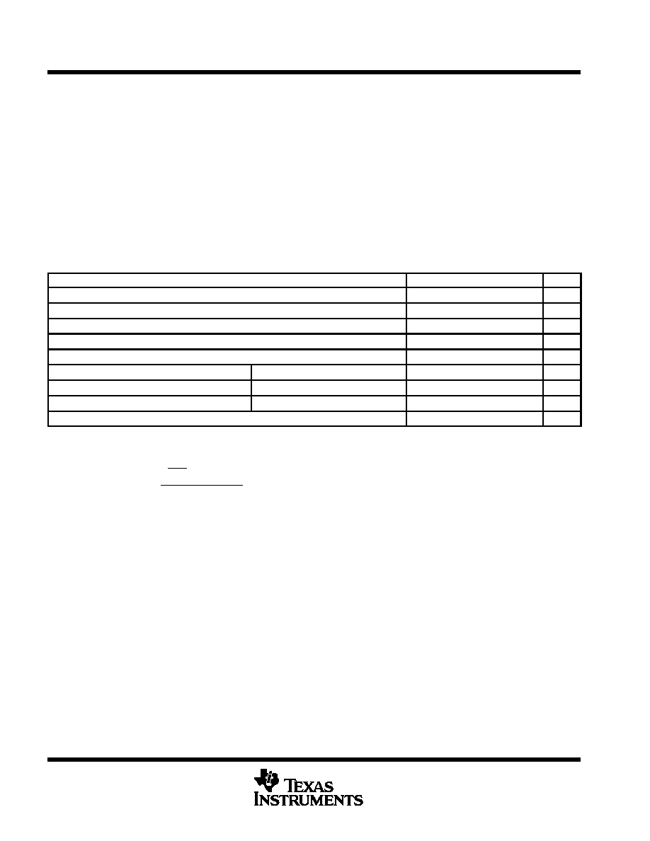
AVAILABLE OPTIONS
PACKAGE
TA
SMALL OUTLINE
(D)
25
°
C to 85
°
C
TLV5590ED
Please be aware that an important notice concerning availability, standard warranty, and use in critical applications of
Texas Instruments semiconductor products and disclaimers thereto appears at the end of this data sheet.
FLEX is a trademark of Motorola, Incorporated.
TLV5591BVF Data Manual Literature Number SLWS048
PRODUCTION DATA information is current as of publication date.
Products conform to specifications per the terms of Texas Instruments
standard warranty. Production processing does not necessarily include
testing of all parameters.
Copyright
©
1996, Texas Instruments Incorporated

TLV5590
2-BIT ANALOG-TO-DIGITAL CONVERTER
FOR FLEX
t PAGER CHIPSET
SLAS134B NOVEMBER 1995 REVISED NOVEMBER 1996
2
POST OFFICE BOX 655303
·
DALLAS, TEXAS 75265
functional block diagram
_
+
8-Bit
DAC
CTR
2-Bit
ADC
fs = 1 kHz
Gain = 12
dB nom.
3rd-Order Butterworth
3rd-Order Butterworth
Mode Control
and Enable
AVDD
MID
Peak Detector
Valley Detector
REF +
REF
EXTS0
EXTS1
DC OFFSET
SIG
CON1
CON2
BW
TRACKINH
11
10
5
2
4
3
8
9
7
12
Up/
Down
CLK
14
fs = 2 kHz
Gain = 12
dB nom.
FILOUT
Decay
Counter
8-Bit
DAC
CTR
Up/
Down
Decay
Counter
TLV5590
2-BIT ANALOG-TO-DIGITAL CONVERTER
FOR FLEX
t PAGER CHIPSET
SLAS134B NOVEMBER 1995 REVISED NOVEMBER 1996
3
POST OFFICE BOX 655303
·
DALLAS, TEXAS 75265
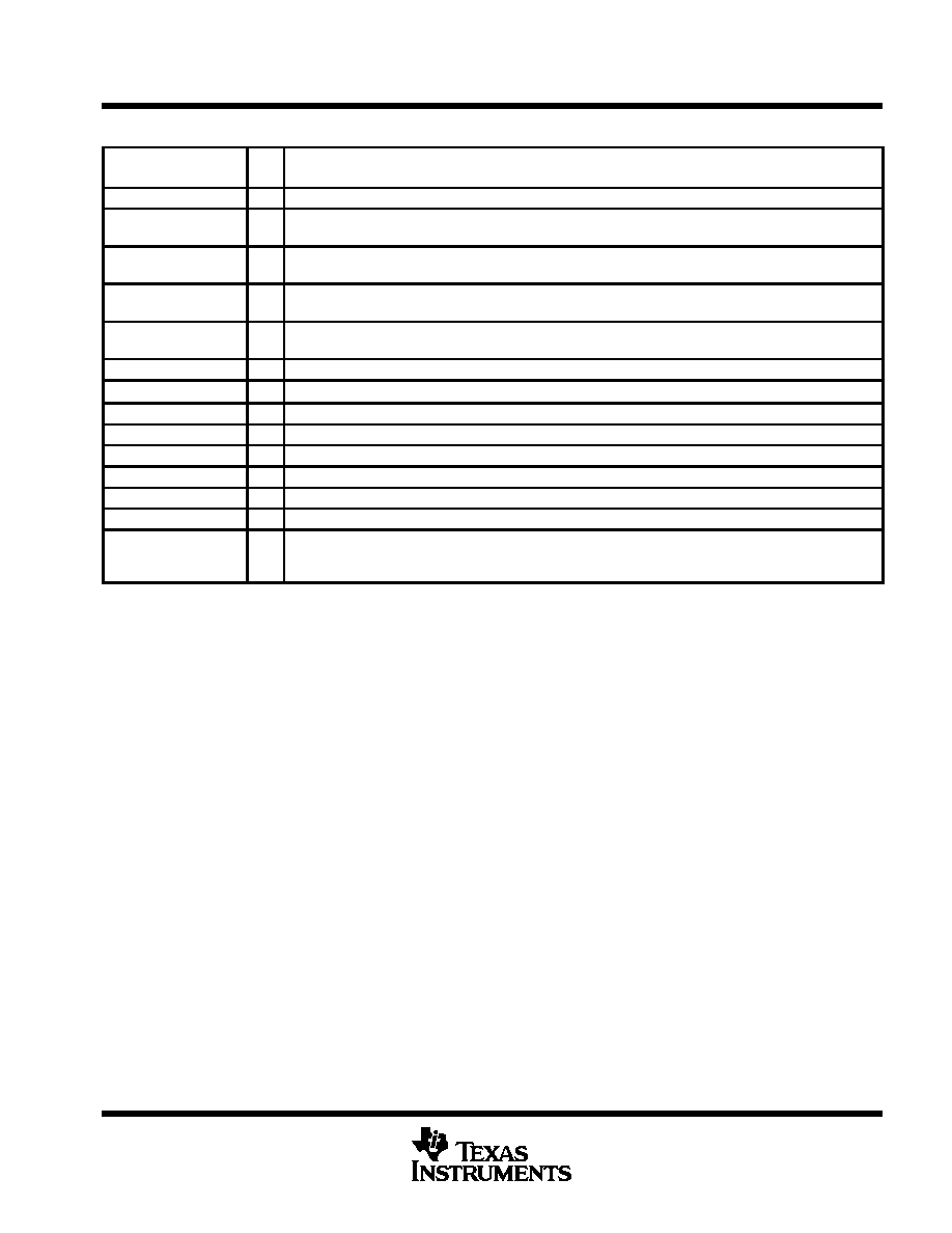
Terminal Functions
TERMINAL
I/O
DESCRIPTION
NAME
NO.
DESCRIPTION
AVDD
2
I
Analog supply voltage
BW
7
I
Digital bandwidth select. A high level on BW selects the 2-kHz filter cutoff and a low level selects the 1-kHz
filter cutoff.
CON1
8
I
Digital control 1 input. In conjunction with CON2, CON1 selects the fast acquisition mode, slow acquisition
mode, hold or standby.
CON2
9
I
Digital control 2 input. In conjunction with CON1, CON2 selects the fast acquisition mode, slow acquisition
mode, hold or standby.
CLK
14
I
Digital clock input. CLK input is a 50% duty cycle TTL-level clock input with nominal frequency of 38.4 kHz.
The CLK input is edge sensitive in all non-test modes. For all test modes, the CLK input is level sensitive.
DC OFFSET
4
I
Analog dc offset correction input. The dc component of the audio signal should be applied to DC OFFSET.
DVDD
1
I
Digital supply voltage
EXTS0
11
O
Digital output 0 of the ADC. Data bit 0 is the LSB.
EXTS1
10
O
Digital output 1 of the ADC. Data bit 1 is the MSB.
GND
6
Return terminal for the IC current.
SIG
3
I
Analog audio signal input. An appropriate RC low-pass filter (antialiasing filter) should be connected to SIG.
MID
5
O
Analog midpoint output. MID is a buffered output of AVDD/2.
TEST
13
I
Digital test input enable. TEST should be connected to ground in normal operation.
TRACKINH
12
I
Digital track inhibit logic input. A high level on TRACKINH disables the peak and valley detector counters, and
a low level enables the peak and valley detector counters. The counters continue to decay at the decay rate
while TRACKINH is a low level.
TLV5590
2-BIT ANALOG-TO-DIGITAL CONVERTER
FOR FLEX
t PAGER CHIPSET
SLAS134B NOVEMBER 1995 REVISED NOVEMBER 1996
4
POST OFFICE BOX 655303
·
DALLAS, TEXAS 75265
absolute maximum ratings over operating free-air temperature range (unless otherwise noted)
Supply voltage range, AV
DD
, DV
DD
0.5 V to 6.5 V
. . . . . . . . . . . . . . . . . . . . . . . . . . . . . . . . . . . . . . . . . . . . . . . . .
Input voltage range, V
I
0.3 V to AV
DD
+ 0.3 V
. . . . . . . . . . . . . . . . . . . . . . . . . . . . . . . . . . . . . . . . . . . . . . . . . . . . .
Output voltage range, EXTS0, EXTS1
0.3 V to DV
DD
+ 0.3 V
. . . . . . . . . . . . . . . . . . . . . . . . . . . . . . . . . . . . . . .
Offset input voltage, V
IO
0.3 V to AV
DD
+ 0.3 V
. . . . . . . . . . . . . . . . . . . . . . . . . . . . . . . . . . . . . . . . . . . . . . . . . . .
Peak input current (any input)
±
20 mA
. . . . . . . . . . . . . . . . . . . . . . . . . . . . . . . . . . . . . . . . . . . . . . . . . . . . . . . . . . . .
Operating free-air temperature range, T
A
25
°
C to 85
°
C
. . . . . . . . . . . . . . . . . . . . . . . . . . . . . . . . . . . . . . . . . . . .
Storage temperature range, T
stg
65
°
C to 150
°
C
. . . . . . . . . . . . . . . . . . . . . . . . . . . . . . . . . . . . . . . . . . . . . . . . . . .
Lead temperature 1,6 mm (1/16 inch) from case for 10 seconds
260
°
C
. . . . . . . . . . . . . . . . . . . . . . . . . . . . . . .
Stresses beyond those listed under "absolute maximum ratings" may cause permanent damage to the device. These are stress ratings only, and
functional operation of the device at these or any other conditions beyond those indicated under "recommended operating conditions" is not
implied. Exposure to absolute-maximum-rated conditions for extended periods may affect device reliability.
recommended operating conditions
MIN
NOM
MAX
UNIT
Supply voltage, AVDD, DVDD
2.7
3.3
V
Power supply ripple
0.002
Vpp
Input clock frequency, f(CLK)
38.4
kHz
Input clock duty cycle
45
50
55
%
Voltage offset applied at DC OFFSET, VI(DC OFFSET) (see Notes 1 and 2)
0.25
VDD0.25
V
Analog input voltage, VI(pp) (See Notes 1 and 2)
VDD = 3.1 V
0.25
VDD 0.25
Vpp
High-level control input voltage, VIH
VDD = 2.7 V to 3.3 V
0.2 DVDD
V
Low-level control input voltage, VIL
VDD = 2.7 V to 3.3 V
0.8 DVDD
V
Operating free-air temperature, TA
25
85
°
C
NOTES:
1. VI(OFFSET) =VQ VI(DC OFFSET) where VQ is the dc quiescent voltage of the signal applied to the SIG terminal.
NOTES:
2.
V
I(PEAK)
+
V
DD
2
*
0.25 V
4.217
*
V
I(OFFSET)
*
80 mV
The pass-band filter gain represents the maximum specified voltage gain in volts/volt of the filter. The maximum gain for the filter
is 4.217 V/V (12.5 dB). The input voltage range from this equation defines the maximum allowable input signal at the SIG terminal
with a given voltage, VI(DC OFFSET), applied at the DC OFFSET terminal and a quiescent dc input voltage, VQ, of the signal applied
at the SIG terminal. When the input voltage is within this range, the peak and valley DACs do not over range. The 80 mV value is
the tolerance on the voltage output at the MID terminal.

TLV5590
2-BIT ANALOG-TO-DIGITAL CONVERTER
FOR FLEX
t PAGER CHIPSET
SLAS134B NOVEMBER 1995 REVISED NOVEMBER 1996
5
POST OFFICE BOX 655303
·
DALLAS, TEXAS 75265
electrical characteristics over recommended operating free-air temperature range,
AV
DD
= DV
DD
= 2.7 V to 3.3 V, f
(CLK)
= 38.4 kHz (unless otherwise noted)
power
PARAMETER
TEST CONDITIONS
MIN
MAX
UNIT
IDD
Operating supply current
Fast track, slow track, or hold mode
250
µ
A
IDD(standby) Standby supply current
VI(DC OFFSET) = 0.8 V,
VI(SIG) = 0.8 V, For all digital inputs,
0 < VI < 0.5 V or VI > DVDD 0.5 V
1
µ
A
digital
PARAMETER
TEST CONDITIONS
MIN
TYP
MAX
UNIT
VOH
High-level output voltage
IOH = 100
µ
A
DVDD 0.5
V
VOL
Low-level output voltage
IOL = 100
µ
A
0.5
V
IIH
High-level input current
VI = DVDD
0.1
1
µ
A
IIL
Low-level input current
VI = 0
0.1
1
µ
A
Ci
Input capacitance, digital input
10
pF
analog
PARAMETER
TEST CONDITIONS
MIN
TYP
MAX
UNIT
Voltage accuracy at MID
VDD = 3 V,
CL(MID) = 220 nF
1.42
1.5
1.58
V
Zi
Input impedance at SIG (see Note 3)
f(IN) = 800 Hz
1
M
Zi(offset)
Input impedance at DC OFFSET (see Note 3)
1
3
M
II(SIG)
Average input current into SIG
GND < VI < AVDD
50
200
nA
Ci
Input capacitance, analog input at SIG
10
pF
NOTE 3: The input is capacitive and, therefore, is dynamic. Impedance specifications are based on f(CLK) = 38.4 kHz.
operating characteristics over recommended operating free-air temperature range,
AV
DD
= DV
DD
= 3 V, f
(CLK)
= 38.4 kHz (unless otherwise noted)
peak-and-valley DACs
PARAMETER
TEST CONDITIONS
MIN
TYP
MAX
UNIT
Step size, LSB
VDD/255
V
EFS
Full-scale error
±
1
LSB
EZS
Zero-code error
±
3
LSB
Voltage output drift
Hold mode
0
mV/ms
ED
Differential linearity error
±
1
LSB
low-pass filter
PARAMETER
TEST CONDITIONS
MIN
TYP
MAX
UNIT
G
Pass band filter gain
VI(DC OFFSET) = 0.8 V, VI =
±
125 mV
11.5
12
12.5
dB
Filter attenuation
1-kHz filter
VI =
±
500 mV
fI(SIG) = 1 kHz
2
3
4
dB
Filter attenuation
2-kHz filter
VI =
±
500 mV
fI(SIG) = 2 kHz
2
3
4
dB
ts
Stabilization time
Off mode to hold mode (see Table 1)
5
ms