
TLV2630, TLV2631
TLV2632, TLV2633
TLV2634, TLV2635
SLOS362A - JUNE 2001 - REVISED JANUARY 2005
FAMILY OF LOW POWER WIDE BANDWIDTH SINGLE SUPPLY
OPERATIONAL AMPLIFIERS WITH AND WITHOUT SHUTDOWN
1
www.ti.com
FEATURES
D
Rail-To-Rail Output
D
V
ICR
Includes Ground
D
Gain-Bandwidth Product . . . 9 MHz
D
Supply Current . . . 730
Á
A/Channel
D
Single, Duals, and Quad Versions
D
Ultralow Power Down Mode
I
DD(SHDN
) = 4
Á
A/Channel
D
Specified Temperature Range
-40
░
C to 125
░
C . . . Industrial Grade
D
Supply Voltage Range . . . 2.7 V to 5.5 V
D
Ultrasmall Packaging
5 or 6 Pin SOT-23 (TLV2630/1)
8 or 10 Pin MSOP (TLV2632/3)
D
Universal Op-Amp EVM (See SLOU060
for More Information)
Operational Amplifier
+
-
DESCRIPTION
The TLV263x single supply operational amplifiers
provide rail-to-rail output with an input range that
includes ground. The TLV263x takes the minimum
operating supply voltage down to 2.7 V over the
extended industrial temperature range (-40
░
C to
125
░
C) while adding the rail-to-rail output swing feature.
The TLV263x also provides a 9 MHz gain-bandwidth
product from only 730
Á
A of supply current. The
maximum recommended supply voltage is 5.5 V, which,
when coupled with a 2.7-V minimum, allows the devices
to be operated from lithium ion cells.
The combination of wide bandwidth, low noise, and low
distortion makes it ideal for high speed and high
resolution data converter applications. The ground
input range allows it to directly interface to ground rail
referred systems.
All members are available in PDIP and SOIC with the
singles in the small SOT-23 package, duals in the
MSOP, and quads in the TSSOP package.
The 2.7-V operation makes it compatible with Li-Ion
powered systems and the operating supply voltage
range of many micro-power microcontrollers available
today including TI's MSP430.
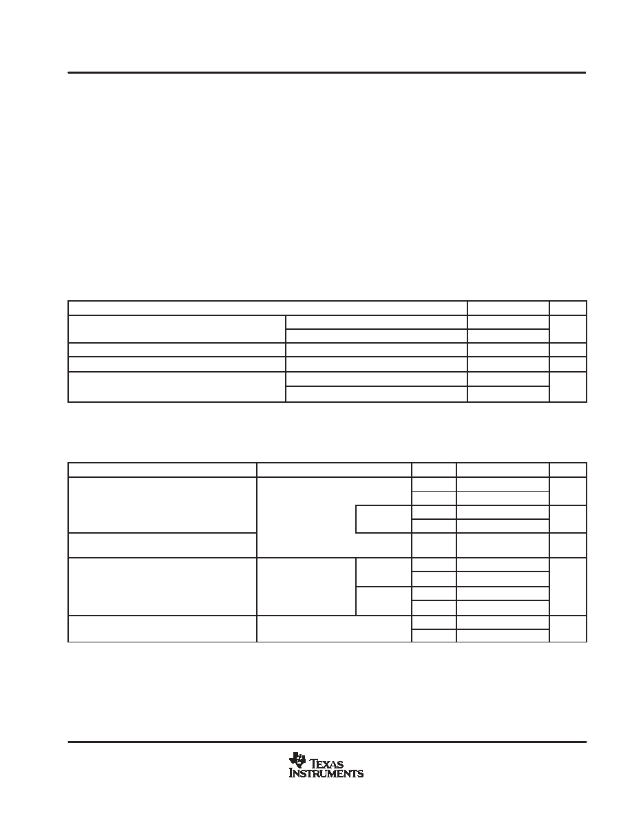
AMPLIFIER SELECTION TABLE
DEVICE
VDD
[V]
IDD/ch
[
Á
A]
VICR
[V]
GBW
[MHz]
SLEW RATE
[V/
Á
s]
Vn, 1 kHz
[nV/
Hz]
IO
[mA]
OPAx343
2.5-5.5
850
-0.3 to VDD + 0.3
5.5
6
25
40
OPAx743
3.5-12
1100
-0.1 to VDD + 0.1
7
10
30
20
TLV278x
1.8-3.6
650
-0.2 to VDD + 0.2
8
5
9
10
TLV263x
2.7-5.5
730
GND to VDD - 1
9
9.5
50
28
TLV262x
2.7-5.5
750
1 V to VDD + 0.2
11
10
27
28
OPAx353
2.7-5.5
8000
-0.1 to VDD + 0.1
44
22
7
40
Copyright
2001-2005, Texas Instruments Incorporated
PRODUCTION DATA information is current as of publication date.
Products conform to specifications per the terms of Texas Instruments
standard warranty. Production processing does not necessarily include
testing of all parameters.
Please be aware that an important notice concerning availability, standard warranty, and use in critical applications of
Texas Instruments semiconductor products and disclaimers thereto appears at the end of this data sheet.

TLV2630, TLV2631
TLV2632, TLV2633
TLV2634, TLV2635
SLOS362A - JUNE 2001 - REVISED JANUARY 2005
2
www.ti.com
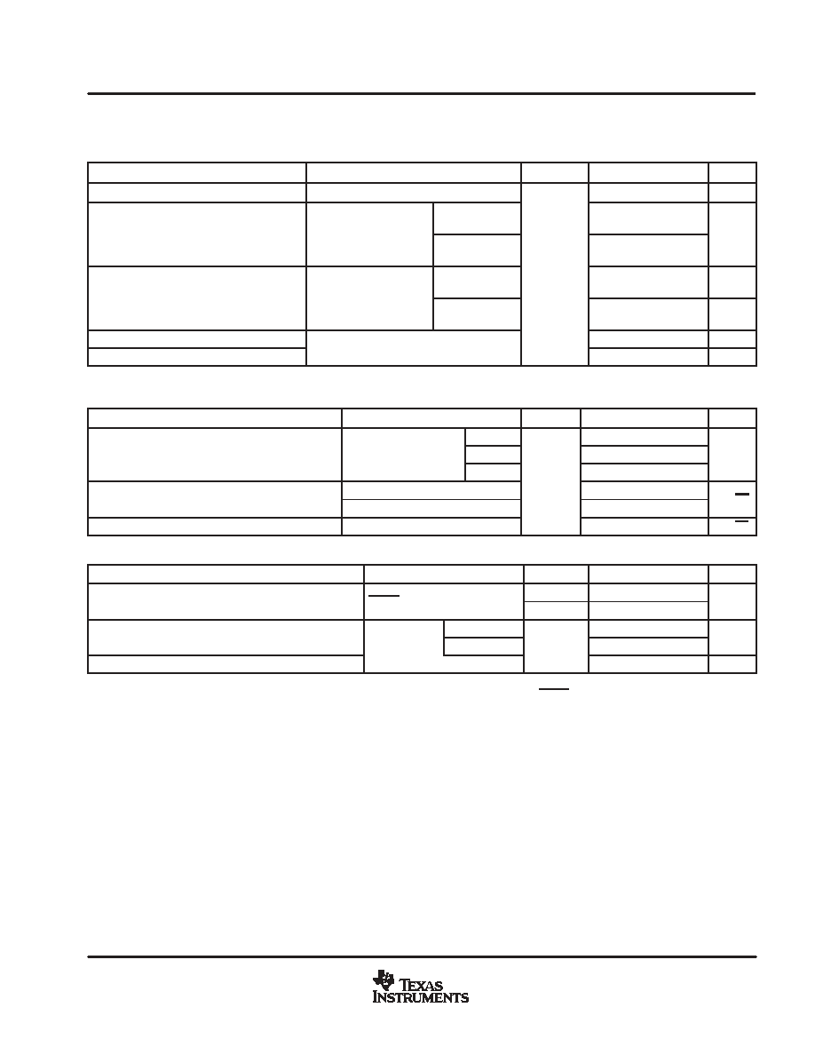
PACKAGE/ORDERING INFORMATION(1)
PRODUCT
PACKAGE
PACKAGE
CODE
SYMBOL
SPECIFIED
TEMPERATURE RANGE
ORDER NUMBER
TRANSPORT MEDIA
Single with Shutdown
TLV2630ID
SOIC-8
D
--
TLV2630ID
TLV2630IDR
Tube
Tape and Reel
TLV2630IDBV
SOT-23-6
DBV
VAYI
-40
░
C to 125
░
C
TLV2630IDBVR
TLV2630IDBVT
Tape and Reel
TLV2630IP
DIP-8
P
--
TLV2630IP
Tube
Single without Shutdown
TLV2631ID
SOIC-8
D
--
TLV2631ID
TLV2631IDR
Tube
Tape and Reel
TLV2631IDBV
SOT-23-5
DBV
VAZI
-40
░
C to 125
░
C
TLV2631IDBVR
TLV2631IDBVT
Tape and Reel
TLV2631IP
DIP-8
P
--
TLV2631IP
Tube
Dual without Shutdown
TLV2632ID
SOIC-8
D
--
TLV2632ID
TLV2632IDR
Tube
Tape and Reel
TLV2632IDGK
MSOP-8
DGK
AKG
-40
░
C to 125
░
C
TLV2632IDGK
TLV2632IDGKR
Tube
Tape and Reel
TLV2632IP
DIP-8
P
--
TLV2632IP
Tube
Dual with Shutdown
TLV2633ID
SOIC-14
D
--
TLV2633ID
TLV2633IDR
Tube
Tape and Reel
TLV2633IDGS
MSOP-10
DGS
AKK
-40
░
C to 125
░
C
TLV2633IDGS
TLV2633IDGSR
Tube
Tape and Reel
TLV2633IN
DIP-14
N
--
TLV2633IN
Tube
Quad without Shutdown
TLV2634ID
SOIC-14
D
--
TLV2634ID
TLV2634IDR
Tube
Tape and Reel
TLV2634IN
DIP-14
N
--
-40
░
C to 125
░
C
TLV2634IN
Tube
TLV2634IPW
TSSOP-14
PW
--
-40 C to 125 C
TLV2634IPW
TLV2634IPWR
Tube
Tape and Reel
Quad with Shutdown
TLV2635ID
SOIC-16
D
--
TLV2635ID
TLV2635IDR
Tube
Tape and Reel
TLV2635IN
DIP-16
N
--
-40
░
C to 125
░
C
TLV2635IN
Tube
TLV2635IPW
TSSOP-16
PW
--
-40 C to 125 C
TLV2635IPW
TLV2635IPWR
Tube
Tape and Reel
The SOT23 package devices are only available taped and reeled. The R Suffix denotes quantities (3,000 pieces per reel).
The T Suffix denotes smaller quantities (250 pieces per mini-reel).
1. For the most current package and ordering information, see the Package Option Addendum at the end of this document, or see the TI
website at www.ti.com.
TLV2630, TLV2631
TLV2632, TLV2633
TLV2634, TLV2635
SLOS362A - JUNE 2001 - REVISED JANUARY 2005
3
www.ti.com
absolute maximum ratings over operating free-air temperature range (unless otherwise noted)
Supply voltage, V
DD
(see Note 1)
6 V
. . . . . . . . . . . . . . . . . . . . . . . . . . . . . . . . . . . . . . . . . . . . . . . . . . . . . . . . . . . . . . . . . .
Differential input voltage, V
ID
▒
V
DD
. . . . . . . . . . . . . . . . . . . . . . . . . . . . . . . . . . . . . . . . . . . . . . . . . . . . . . . . . . . . . . . . . . . .
Input voltage range, V
I
(see Note 1)
GND to V
DD
- 1 V
. . . . . . . . . . . . . . . . . . . . . . . . . . . . . . . . . . . . . . . . . . . . . . . . . . .
Input current, I
I
(any input)
▒
10 mA
. . . . . . . . . . . . . . . . . . . . . . . . . . . . . . . . . . . . . . . . . . . . . . . . . . . . . . . . . . . . . . . . . . . . .
Output current, I
O
▒
40 mA
. . . . . . . . . . . . . . . . . . . . . . . . . . . . . . . . . . . . . . . . . . . . . . . . . . . . . . . . . . . . . . . . . . . . . . . . . . . .
Continuous total power dissipation
See Dissipation Rating Table
. . . . . . . . . . . . . . . . . . . . . . . . . . . . . . . . . . . . . . . . . .
Operating free-air temperature range, T
A
: I-suffix
-40
░
C to 125
░
C
. . . . . . . . . . . . . . . . . . . . . . . . . . . . . . . . . . . . . . . . .
Maximum junction temperature, T
J
150
░
C
. . . . . . . . . . . . . . . . . . . . . . . . . . . . . . . . . . . . . . . . . . . . . . . . . . . . . . . . . . . . . .
Storage temperature range, T
stg
-65
░
C to 150
░
C
. . . . . . . . . . . . . . . . . . . . . . . . . . . . . . . . . . . . . . . . . . . . . . . . . . . . . . . .
Lead temperature 1,6 mm (1/16 inch) from case for 10 seconds
260
░
C
. . . . . . . . . . . . . . . . . . . . . . . . . . . . . . . . . . . . .
Stresses beyond those listed under "absolute maximum ratings" may cause permanent damage to the device. These are stress ratings only, and
functional operation of the device at these or any other conditions beyond those indicated under "recommended operating conditions" is not
implied. Exposure to absolute-maximum-rated conditions for extended periods may affect device reliability.
NOTE 2: All voltage values, except differential voltages, are with respect to GND.
recommended operating conditions
MIN
MAX
UNIT
Supply voltage, VDD
Single supply
2.7
5.5
V
Supply voltage, VDD
Split supply
▒
1.35
▒
2.75
V
Common-mode input voltage range, VICR
GND
VDD-1
V
Operating free-air temperature, TA
I-suffix
- 40
125
░
C
Shutdown on/off voltage level
VIL
0.4
V
Shutdown on/off voltage level
VIH
2
V
Relative to GND.
electrical characteristics at specified free-air temperature, V
DD
= 2.7 V, 5 V (unless otherwise noted)
dc performance
PARAMETER
TEST CONDITIONS
TA
MIN
TYP
MAX
UNIT
25
░
C
250
3500
V
VIO
Input offset voltage
Full range
4500
Á
V
VIO
Input offset voltage
VIC = VDD/2,
V = V
/2
TLV2634/5
25
░
C
250
4200
V
VIC = VDD/2,
VO = VDD/2
TLV2634/5
Full range
5200
Á
V
VIO
Temperature coefficient of input offset
voltage
O
DD
25
░
C
3
Á
V/
░
C
VDD = 2.7 V
25
░
C
76
100
CMRR
Common-mode rejection ratio
VIC = GND to VDD-1 V
VDD = 2.7 V
Full range
67
dB
CMRR
Common-mode rejection ratio
VIC = GND to VDD-1 V
VDD = 5 V
25
░
C
77
100
dB
VDD = 5 V
Full range
74
AVD
Large-signal differential voltage
RL = 2 k
, VO(PP) = VDD-1 V
25
░
C
90
100
dB
AVD
Large-signal differential voltage
amplification
RL = 2 k
, VO(PP) = VDD-1 V
Full range
82
dB

TLV2630, TLV2631
TLV2632, TLV2633
TLV2634, TLV2635
SLOS362A - JUNE 2001 - REVISED JANUARY 2005
4
www.ti.com
electrical characteristics at specified free-air temperature, V
DD
= 2.7 V, 5 V (unless otherwise noted)
(continued)
input characteristics
PARAMETER
TEST CONDITIONS
TA
MIN
TYP
MAX
UNIT
IIO
Input offset current
25
░
C
1
50
IIO
Input offset current
VIC = VDD/2,
Full range
100
pA
IIB
Input bias current
VIC = VDD/2,
VO = VDD/2
25
░
C
1
50
pA
IIB
Input bias current
VO = VDD/2
Full range
200
ri(d)
Differential input resistance
25
░
C
1000
G
Ci(c)
Common-mode input capacitance
f = 1 kHz
25
░
C
12
pF
Full range is -40
░
C to 125
░
C for the I-suffix.
output characteristics
PARAMETER
TEST CONDITIONS
TA
MIN
TYP
MAX
UNIT
VDD = 2.7 V
25
░
C
2.6
2.67
VIC = VDD/2, IOH = - 1 mA
VDD = 2.7 V
Full range
2.55
VIC = VDD/2, IOH = - 1 mA
VDD = 5 V
25
░
C
4.92
4.98
VOH
High-level output voltage
VDD = 5 V
Full range
4.9
V
VOH
High-level output voltage
VDD = 2.7 V
25
░
C
2.25
2.43
V
VIC = VDD/2, IOH = - 10 mA
VDD = 2.7 V
Full range
2.15
VIC = VDD/2, IOH = - 10 mA
VDD = 5 V
25
░
C
4.7
4.8
VDD = 5 V
Full range
4.65
VDD = 2.7 V
25
░
C
0.03
0.1
VIC = VDD/2, IOL = 1 mA
VDD = 2.7 V
Full range
0.15
VIC = VDD/2, IOL = 1 mA
VDD = 5 V
25
░
C
0.025
0.08
VOL
Low-level output voltage
VDD = 5 V
Full range
0.1
mV
VOL
Low-level output voltage
VDD = 2.7 V
25
░
C
0.26
0.45
mV
VIC = VDD/2, IOL = 10 mA
VDD = 2.7 V
Full range
0.47
VIC = VDD/2, IOL = 10 mA
VDD = 5 V
25
░
C
0.2
0.3
VDD = 5 V
Full range
0.35
VDD = 2.7 V,
Sourcing
14
IO
Output current
VDD = 2.7 V,
VO = 0.5 V from rail
Sinking
25
░
C
19
mA
IO
Output current
VDD = 5 V,
Sourcing
25
░
C
28
mA
VDD = 5 V,
VO = 0.5 V from rail
Sinking
28
Sourcing
VDD = 2.7 V
50
IOS
Short-circuit output current
Sourcing
VDD = 5 V
25
░
C
95
mA
IOS
Short-circuit output current
Sinking
VDD = 2.7 V
25
░
C
50
mA
Sinking
VDD = 5 V
95
Full range is -40
░
C to 125
░
C for the I-suffix.
power supply
PARAMETER
TEST CONDITIONS
TA
MIN
TYP
MAX
UNIT
IDD
Supply current (per channel)
VO = VDD/2,
SHDN = VDD
25
░
C
730
1000
A
IDD
Supply current (per channel)
VO = VDD/2,
SHDN = VDD
Full range
1350
Á
A
PSRR
Supply voltage rejection ratio
VDD = 2.7 V to 5.5 V,
No load
25
░
C
70
90
dB
PSRR
Supply voltage rejection ratio
(
VDD /
VIO)
VDD = 2.7 V to 5.5 V,
VIC = VDD /2
No load
Full range
65
dB
Full range is -40
░
C to 125
░
C for the I-suffix.
TLV2630, TLV2631
TLV2632, TLV2633
TLV2634, TLV2635
SLOS362A - JUNE 2001 - REVISED JANUARY 2005
5
www.ti.com
electrical characteristics at specified free-air temperature, V
DD
= 2.7 V, 5 V (unless otherwise noted)
(continued)
dynamic performance
PARAMETER
TEST CONDITIONS
TA
MIN
TYP
MAX
UNIT
GBWP
Gain-bandwidth product
RL = 2 k
, CL = 10 pF, f = 10 kHz
9
MHz
SR+
Positive slew rate at unity gain
RL = 2 k
CL = 50 pF
VDD = 2.7 V,
VO(PP) = 1.7 V
6
V/ s
SR+
Positive slew rate at unity gain
RL = 2 k
,
CL = 50 pF
VDD = 5 V,
VO(PP) = 3.5 V
6
V/
Á
s
SR-
Negative slew rate at unity gain
RL = 2 k
CL = 50 pF
VDD = 2.7 V,
VO(PP) = 1.7 V
25
░
C
10
V/
Á
s
SR-
Negative slew rate at unity gain
RL = 2 k
,
CL = 50 pF
VDD = 5 V,
VO(PP) = 3.5 V
9.5
V/
Á
s
m
Phase margin
RL = 2 k
,
CL = 10 pF
50
░
Gain margin
RL = 2 k
,
CL = 10 pF
20
dB
Full range is -40
░
C to 125
░
C for the I-suffix.
noise/distortion performance
PARAMETER
TEST CONDITIONS
TA
MIN
TYP
MAX
UNIT
VO(PP) = VDD/2,
AV = 1
0.003%
THD + N
Total harmonic distortion plus noise
VO(PP) = VDD/2,
RL = 2 k
, f = 10 kHz
AV = 10
0.02%
THD + N
Total harmonic distortion plus noise
RL = 2 k
, f = 10 kHz
AV = 100
25
░
C
0.095%
Vn
Equivalent input noise voltage
f = 1 kHz
25
░
C
50
nV/
Hz
Vn
Equivalent input noise voltage
f = 10 kHz
30
nV/
Hz
In
Equivalent input noise current
f = 1 kHz
0.9
fA /
Hz
shutdown characteristics
PARAMETER
TEST CONDITIONS
TA
MIN
TYP
MAX
UNIT
IDD(SHDN)
Supply current, per channel in shutdown
SHDN = 0.4 V
25
░
C
4
17
A
IDD(SHDN)
Supply current, per channel in shutdown
mode (TLV2630, TLV2633, TLV2635)
SHDN = 0.4 V
Full range
19
Á
A
t(on)
Amplifier turnon time
RL = 2 k
VDD = 2.7 V
4.5
s
t(on)
Amplifier turnon time
RL = 2 k
,
CL = 10 pF
VDD = 5 V
25
░
C
1.5
Á
s
t(off)
Amplifier turnoff time
CL = 10 pF
25 C
200
ns
Full range is -40
░
C to 125
░
C for the I-suffix.
Disable time and enable time are defined as the interval between application of the logic signal to SHDN and the point at which the supply current
has reached half its final value.