TLV2544, TLV2548
2.7 V TO 5.5 V, 12-BIT, 200 KSPS, 4/8 CHANNEL, LOW POWER,
SERIAL ANALOG-TO-DIGITAL CONVERTERS WITH AUTO POWER DOWN
SLAS198A ÙFEBRUARY 1999Ù REVISED AUGUST 1999
1
POST OFFICE BOX 655303
ñ
DALLAS, TEXAS 75265
D
Maximum Throughput 200 KSPS
D
Built-In Reference, Conversion Clock and
8
æ
FIFO
D
Differential/Integral Nonlinearity Error:
Ý
1 LSB
D
Signal-to-Noise and Distortion Ratio:
69 dB, f
i
= 12 kHz
D
Spurious Free Dynamic Range: 75 dB,
f
i
= 12 kHz
D
SPI/DSP-Compatible Serial Interfaces With
SCLK up to 20 MHz
D
Single Wide Range Supply 2.7 Vdc to
5.5 Vdc
D
Analog Input Range 0 V to Supply Voltage
with 500 kHz BW
D
Hardware Controlled and Programmable
Sampling Period
D
Low Operating Current (1 mA at 2.7 V,
1.2 mA at 5.5 V External Ref,
1.6 mA at 2.7 V,
2.1 mA at 5.5 V, Internal Ref)
D
Power Down: Software/Hardware
Power-Down Mode (1
ç
A Max, Ext Ref),
Auto Power-Down Mode (1
ç
A, Ext Ref)
D
Programmable Auto-Channel Sweep
1
2
3
4
5
6
7
8
9
10
20
19
18
17
16
15
14
13
12
11
SDO
SDI
SCLK
EOC/(INT)
V
CC
A0
A1
A2
A3
A4
CS
REFP
REFM
FS
PWDN
GND
CSTART
A7
A6
A5
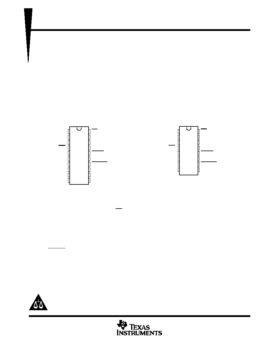
DW OR PW PACKAGE
1
2
3
4
5
6
7
8
16
15
14
13
12
11
10
9
SDO
SDI
SCLK
EOC/(INT)
V
CC
A0
A1
A2
CS
REFP
REFM
FS
PWDN
GND
CSTART
A3
D OR PW PACKAGE
(TOP VIEW)
(TOP VIEW)
description
The TLV2548 and TLV2544 are a family of high performance, 12-bit low power, 3.6
ç
s, CMOS analog-to-digital
converters (ADC) which operate from a single 2.7 V to 5.5 V power supply. These devices have three digital
inputs and a 3-state output [chip select (CS), serial input-output clock (SCLK), serial data input (SDI) and serial
data output (SDO)] that provide a direct 4-wire interface to the serial port of most popular host microprocessors
(SPI interface). When interfaced with a DSP, a frame sync (FS) signal is used to indicate the start of a serial data
frame.
In addition to a high-speed A/D converter and versatile control capability, these devices have an on-chip analog
multiplexer that can select any analog inputs or one of three internal self-test voltages. The sample-and-hold
function is automatically started after the fourth SCLK edge (normal sampling) or can be controlled by a special
pin, CSTART, to extend the sampling period (extended sampling). The normal sampling period can also be
programmed as short (12 SCLKs) or as long (24 SCLKs) to accommodate faster SCLK operation popular
among high-performance signal processors. The TLV2548 and TLV2544 are designed to operate with very low
power consumption. The power-saving feature is further enhanced with software/hardware/auto power down
modes and programmable conversion speeds. The conversion clock (OSC) and reference are built-in. The
converter can use the external SCLK as the source of the conversion clock to achieve higher (up to 3.6
ç
s when
a 20 MHz SCLK is used) conversion speed. Two different internal reference voltages are available. An optional
external reference can also be used to achieve maximum flexibility.
Copyright
ˋ
1999, Texas Instruments Incorporated
PRODUCTION DATA information is current as of publication date.
Products conform to specifications per the terms of Texas Instruments
standard warranty. Production processing does not necessarily include
testing of all parameters.
Please be aware that an important notice concerning availability, standard warranty, and use in critical applications of
Texas Instruments semiconductor products and disclaimers thereto appears at the end of this data sheet.

TLV2544, TLV2548
2.7 V TO 5.5 V, 12-BIT, 200 KSPS, 4/8 CHANNEL, LOW POWER,
SERIAL ANALOG-TO-DIGITAL CONVERTERS WITH AUTO POWER DOWN
SLAS198A ÙFEBRUARY 1999Ù REVISED AUGUST 1999
2
POST OFFICE BOX 655303
ñ
DALLAS, TEXAS 75265
functional block diagram
Command
Decode
SDI
CS
FS
EOC/(INT)
Low Power
12-BIT
SAR ADC
Control Logic
CSTART
PWDN
VCC
GND
REFP
Analog
MUX
4/2 V
Reference
S/H
OSC
Conversion
Clock
M
U
X
FIFO
12 Bit
æ
8
CFR
SCLK
SDO
2548
A0
A1
A2
A3
A4
A5
A6
A7
REFM
2544
A0
X
A1
X
A2
X
A3
X
CMR (4 MSBs)
AVAILABLE OPTIONS
PACKAGED DEVICES
TA
20-TSSOP
(PW)
20-SOIC
(DW)
16-SOIC
(D)
16-TSSOP
(PW)
0
¯
C to 70
¯
C
TLV2548CPW
TLV2548CDW
TLV2544CD
TLV2544CPW
Ù 40
¯
C to 85
¯
C
TLV2548IPW
TLV2548IDW
TLV2544ID
TLV2544IPW
TLV2544, TLV2548
2.7 V TO 5.5 V, 12-BIT, 200 KSPS, 4/8 CHANNEL, LOW POWER,
SERIAL ANALOG-TO-DIGITAL CONVERTERS WITH AUTO POWER DOWN
SLAS198A ÙFEBRUARY 1999Ù REVISED AUGUST 1999
3
POST OFFICE BOX 655303
ñ
DALLAS, TEXAS 75265
Terminal Functions
TERMINAL
NAME
NO.
I/O
DESCRIPTION
NAME
TLV2544
TLV2548
A0
A0
A1
A1
A2
A2
A3
A3
A4
A5
A6
A7
6
7
8
9
6
7
8
9
10
11
12
13
I
Analog signal inputs. The analog inputs are applied to these terminals and are internally
multiplexed. The driving source impedance should be less than or equal to 1 k
.
For a source impedance greater than 1 k
, use the asynchronous conversion start signal CSTART
(CSTART low time controls the sampling period) or program long sampling period to increase the
sampling time.
CS
16
20
I
Chip select. A high-to-low transition on the CS input resets the internal 4-bit counter, enables SDI,
and removes SDO from 3-state within a maximum setup time. SDI is disabled within a setup time
after the 4-bit counter counts to 16 (clock edges) or a low-to-high transition of CS whichever
happens first. SDO is 3-stated after the rising edge of CS.
CS can be used as the FS pin when a dedicated serial port is used.
CSTART
10
14
I
This terminal controls the start of sampling of the analog input from a selected multiplex channel.
A high-to-low transition starts sampling of the analog input signal. A low-to-high transition puts the
S/H in hold mode and starts the conversion. This input is independent from SCLK and works when
CS is high (inactive). The low time of CSTART controls the duration of the sampling period of the
converter (extended sampling).
Tie this terminal to VCC if not used.
EOC/(INT)
4
4
O
End of conversion or interrupt to host processor.
[PROGRAMMED AS EOC]: This output goes from a high-to-low logic level at the end of the
sampling period and remains low until the conversion is complete and data are ready for transfer.
EOC is used in conversion mode 00 only.
[PROGRAMMED AS INT]: This pin can also be programmed as an interrupt output signal to the
host processor. The falling edge of INT indicates data are ready for output. The following CS
or
FS
clears INT. The falling edge of INT puts SDO back to 3-state even if CS is still active.
FS
13
17
I
DSP frame sync input. Indication of the start of a serial data frame in or out of the device. If FS
remains low after the falling edge of CS, SDI is not enabled until an active FS is presented. A
high-to-low transition on the FS input resets the internal 4-bit counter and enables SDI within a
maximum setup time. SDI is disabled within a setup time after the 4-bit counter counts to 16 (clock
edges) or a low-to-high transition of CS whichever happens first. SDO is 3-stated after the 16th bit
is presented.
Tie this terminal to VCC if not used.
GND
11
15
I
Ground return for the internal circuitry. Unless otherwise noted, all voltage measurements are with
respect to GND.
PWDN
12
16
I
Both analog and reference circuits are powered down when this pin is at logic zero. The device can
be restarted by active CS or CSTART after this pin is pulled back to logic one.
SCLK
3
3
I
Input serial clock. This terminal receives the serial SCLK from the host processor. SCLK is used to
clock the input SDI to the input register. When programmed, it may also be used as the source of
the conversion clock.
SDI
2
2
I
Serial data input. The input data is presented with the MSB (D15) first. The first 4-bit MSBs,
D(15Ù12) are decoded as one of the 16 commands (12 only for the TLV2544). All trailing blanks are
filled with zeros. The configure write commands require an additional 12 bits of data.
When FS is not used (FS =1), the first MSB (D15) is expected after the falling edge of CS and is
shifted in on the rising edges of SCLK (after CS
).
When FS is used (typical with an active FS from a DSP) the first MSB (D15) is expected after the
falling edge of FS and is shifted in on the falling edges of SCLK.
TLV2544, TLV2548
2.7 V TO 5.5 V, 12-BIT, 200 KSPS, 4/8 CHANNEL, LOW POWER,
SERIAL ANALOG-TO-DIGITAL CONVERTERS WITH AUTO POWER DOWN
SLAS198A ÙFEBRUARY 1999Ù REVISED AUGUST 1999
4
POST OFFICE BOX 655303
ñ
DALLAS, TEXAS 75265
Terminal Functions (Continued)
TERMINAL
NAME
NO.
I/O
DESCRIPTION
NAME
TLV2544
TLV2548
SDO
1
1
O
The 3-state serial output for the A/D conversion result. SDO is kept in the high-impedance state
when CS is high and after the CS falling edge and until the MSB (D15) is presented. The output
format is MSB (D15) first.
When FS is not used (FS = 1 at the falling edge of CS), the MSB (D15) is presented to the SDO pin
after the CS falling edge, and successive data are available at the rising edge of SCLK.
When FS is used (FS = 0 at the falling edge of CS), the MSB (D15) is presented to SDO after the
falling edge of CS and FS = 0 is detected. Successive data are available at the falling edge of SCLK.
(This is typically used with an active FS from a DSP.)
For conversion and FIFO read cycles, the first 12 bits are result from previous conversion (data)
followed by 4 trailing zeros. The first four bits from SDO for CFR read cycles should be ignored. The
register content is in the last 12 bits. SDO is 3 stated after the 16th bit.
REFM
14
18
I
External reference input or internal reference decoupling.
REFP
15
19
I
External reference input or internal reference decoupling. (Shunt capacitors of 10
ç
F and 0.1
ç
F
between REFP and REFM.) The maximum input voltage range is determined by the difference
between the voltage applied to this terminal and the REFM terminal when an external reference is
used.
VCC
5
5
I
Positive supply voltage
detailed description
analog inputs and internal test voltages
The 4/8 analog inputs and three internal test inputs are selected by the analog multiplexer depending on the
command entered. The input multiplexer is a break-before-make type to reduce input-to-input noise injection
resulting from channel switching.
converter
The TLV2544/48 uses a 12-bit successive approximation ADC utilizing a charge redistribution DAC. Figure 1
shows a simplified version of the DAC.
The sampling capacitor acquires the signal on Ain during the sampling period. When the conversion process
starts, the SAR control logic and charge redistribution DAC are used to add and subtract fixed amounts of charge
from the sampling capacitor to bring the comparator into a balanced condition. When the comparator is
balanced, the conversion is complete and the ADC output code is generated.
TLV2544, TLV2548
2.7 V TO 5.5 V, 12-BIT, 200 KSPS, 4/8 CHANNEL, LOW POWER,
SERIAL ANALOG-TO-DIGITAL CONVERTERS WITH AUTO POWER DOWN
SLAS198A ÙFEBRUARY 1999Ù REVISED AUGUST 1999
5
POST OFFICE BOX 655303
ñ
DALLAS, TEXAS 75265
detailed description (continued)
Charge
Redistribution
DAC
Control
Logic
_
+
REFM
Ain
ADC Code
Figure 1. Simplified Model of the Successive-Approximation System
serial interface
INPUT DATA FORMAT
MSB
LSB
D15ÙD12
D11ÙD0
Command
Configuration data field
Input data is binary. All trailing blanks can be filled with zeros.
OUTPUT DATA FORMAT READ CFR
MSB
LSB
D15ÙD12
D11ÙD0
Don't care
Register content
OUTPUT DATA FORMAT CONVERSION/READ FIFO
MSB
LSB
D15ÙD4
D3ÙD0
Conversion result
All zeros
The output data format is binary (unipolar straight binary).
binary
Zero scale code = 000h, Vcode = VREFM
Full scale code = FFFh, Vcode = VREFP Ù 1 LSB