Document Outline
- FEATURES
- APPLICATIONS
- DESCRIPTION
- PACKAGE/ORDERING INFORMATION
- absolute maximum ratings over operating free-air temperature (unless otherwise noted)ü
- DISSIPATION RATING TABLE
- recommended operating conditions
- electrical characteristics at recommended operating conditions, VS = 2.7 V, 5 V, and 15 V ( unless otherwise noted)
- dc performance
- input characteristics
- power supply
- output characteristics
- dynamic performance
- noise/distortion performance
- TYPICAL CHARACTERISTICS
- APPLICATION INFORMATION
- offset voltage
- general configurations
- circuit layout considerations
- general power dissipation considerations
- IMPORTANT NOTICE
TLV2381
TLV2382
SLOS377A ş SEPTEMBER 2001ş REVISED JULY 2003
FAMILY OF MICROPOWER RAIL-TO-RAIL INPUT AND OUTPUT
OPERATIONAL AMPLIFIERS
1
www.ti.com
FEATURES
D
BiMOS Rail-to-Rail Input/Output
D
Input Bias Current . . . 1 pA
D
High Wide Bandwidth . . . 160 kHz
D
High Slew Rate . . . 0.1 V/
Á
s
D
Supply Current . . . 7
Á
A (per channel)
D
Input Noise Voltage . . . 90 nV/
Hz
D
Supply Voltage Range . . . 2.7 V to 16 V
D
Specified Temperature Range
ş ş40
░
C to 125
░
C . . . Industrial Grade
D
Ultra-Small Packaging
ş 5 Pin SOT-23 (TLV2381)
APPLICATIONS
D
Portable Medical
D
Power Monitoring
D
Low Power Security Detection Systems
D
Smoke Detectors
DESCRIPTION
The TLV238x single supply operational amplifiers
provide rail-to-rail input and output capability. The
TLV238x takes the minimum operating supply voltage
down to 2.7 V over the extended industrial temperature
range, while adding the rail-to-rail output swing feature.
The TLV238x also provides 160-kHz bandwidth from
only 7
Á
A. The maximum recommended supply voltage
is 16 V, which allows the devices to be operated from
(
▒
8 V supplies down to
▒
1.35 V) two rechargeable cells.
The combination of rail-to-rail inputs and outputs make
them good upgrades for the TLC27Lx family--offering
more bandwidth at a lower quiescent current. The offset
voltage is lower than the TLC27LxA variant.
To maintain cost effectiveness the TLV2381/2 are only
available in the extended industrial temperature range.
This means that one device can be used in a wide range
of applications that include PDAs as well as automotive
sensor interface.
All members are available in SOIC, with the singles in
the small SOT-23 package, duals in the MSOP.
SELECTION GUIDE
DEVICE
VS
[V]
IQ/ch
[
Á
A]
VICR
[V]
VIO
[mV]
IIB
[pA]
GBW
[MHz]
SLEW RATE
[V/
Á
s]
Vn, 1 kHz
[nV/
Hz]
TLV238x
2.7 to 16
10
ş0.2 to VS + 0.2
4.5
60
0.16
0.06
100
TLV27Lx
2.7 to 16
11
ş0.2 to VS ş 1.2
5
60
0.16
0.06
100
TLC27Lx
4 to 16
17
ş0.2 to VS ş 1.5
10/5/2
60
0.085
0.03
68
OPAx349
1.8 to 5.5
2
ş0.2 to VS + 0.2
10
10
0.070
0.02
300
OPAx347
2.3 to 5.5
34
ş0.2 to VS + 0.2
6
10
0.35
0.01
60
TLC225x
2.7 to 16
62.5
0 to VS ş 1.5
1.5/0.85
60
0.200
0.02
19
NOTE: All dc specs are maximums while ac specs are typicals.
PRODUCTION DATA information is current as of publication date.
Products conform to specifications per the terms of Texas Instruments
standard warranty. Production processing does not necessarily include
testing of all parameters.
Copyright
2001ş2003 Texas Instruments Incorporated
Please be aware that an important notice concerning availability, standard warranty, and use in critical applications of
Texas Instruments semiconductor products and disclaimers thereto appears at the end of this data sheet.
TLV2381
TLV2382
SLOS377A ş SEPTEMBER 2001ş REVISED JULY 2003
2
www.ti.com
PACKAGE/ORDERING INFORMATION
PRODUCT
PACKAGE
PACKAGE
CODE
SYMBOL
SPECIFIED
TEMPERATURE
RANGE
ORDER NUMBER
TRANSPORT MEDIA
TLV2381ID
SOIC-8
D
2381I
ş40 C to 125 C
TLV2381ID
Tube
TLV2381ID
SOIC-8
D
2381I
ş40 C to 125 C
TLV2381IDR
Tape and Reel
TLV2381IDBV
SOT-23
DBV
VBKI
ş40
░
C to 125
░
C
TLV2381IDBVR
Tape and Reel
TLV2381IDBV
SOT-23
DBV
VBKI
ş40
░
C to 125
░
C
TLV2381IDBVT
Tape and Reel
TLV2382ID
SOIC-8
D
2382I
TLV2382ID
Tube
TLV2382ID
SOIC-8
D
2382I
TLV2382IDR
Tape and Reel
absolute maximum ratings over operating free-air temperature (unless otherwise noted)
Supply voltage, V
S
16.5 V
. . . . . . . . . . . . . . . . . . . . . . . . . . . . . . . . . . . . . . . . . . . . . . . . . . . . . . . . . . . . . . . . . . . . . . . . . . . .
Input voltage, V
I
(see Notes 1 and 2)
V
S
+ 0.2 V
. . . . . . . . . . . . . . . . . . . . . . . . . . . . . . . . . . . . . . . . . . . . . . . . . . . . . . . .
Output current, I
O
100 mA
. . . . . . . . . . . . . . . . . . . . . . . . . . . . . . . . . . . . . . . . . . . . . . . . . . . . . . . . . . . . . . . . . . . . . . . . . . . .
Differential input voltage, V
ID
V
S
. . . . . . . . . . . . . . . . . . . . . . . . . . . . . . . . . . . . . . . . . . . . . . . . . . . . . . . . . . . . . . . . . . . . . .
Continuous total power dissipation
See Dissipation Rating Table
. . . . . . . . . . . . . . . . . . . . . . . . . . . . . . . . . . . . . . . . . .
Maximum junction temperature, T
J
150
░
C
. . . . . . . . . . . . . . . . . . . . . . . . . . . . . . . . . . . . . . . . . . . . . . . . . . . . . . . . . . . . . .
Operating free-air temperature range, T
A
: I suffix
ş40
░
C to 125
░
C
. . . . . . . . . . . . . . . . . . . . . . . . . . . . . . . . . . . . . . . . .
Storage temperature range, T
stg
ş65
░
C to 125
░
C
. . . . . . . . . . . . . . . . . . . . . . . . . . . . . . . . . . . . . . . . . . . . . . . . . . . . . . .
Lead temperature 1,6 mm (1/16 inch) from case for 10 seconds
300
░
C
. . . . . . . . . . . . . . . . . . . . . . . . . . . . . . . . . . . . .
Stresses beyond those listed under "absolute maximum ratings" may cause permanent damage to the device. These are stress ratings only, and
functional operation of the device at these or any other conditions beyond those indicated under "recommended operating conditions" is not
implied. Exposure to absolute-maximum-rated conditions for extended periods may affect device reliability.
NOTES:
1. Relative to GND pin.
2. Maximum is 16.5 V or VS+0.2 V whichever is the lesser value.
DISSIPATION RATING TABLE
PACKAGE
JC
(
░
C/W)
JA
(
░
C/W)
TA
25
░
C
POWER RATING
TA = 85
░
C
POWER RATING
D (8)
38.3
176
710 mW
370 mW
DBV (5)
55
324.1
385 mW
201 mW
DBV (6)
55
294.3
425 mW
221 mW

TLV2381
TLV2382
SLOS377A ş SEPTEMBER 2001ş REVISED JULY 2003
3
www.ti.com
recommended operating conditions
MIN
MAX
UNIT
Supply voltage, (VS)
Dual supply
▒
1.35
▒
8
V
Supply voltage, (VS)
Single supply
2.7
16
V
Input common-mode voltage range
ş0.2
VS+0.2
V
Operating free air temperature, TA
I-suffix
ş40
125
░
C
electrical characteristics at recommended operating conditions, V
S
= 2.7 V, 5 V, and 15 V (unless
otherwise noted)
dc performance
PARAMETER
TEST CONDITIONS
TA
MIN
TYP
MAX
UNIT
VIO
Input offset voltage
VIC = VS/2,
VO = VS/2
25
░
C
0.5
4.5
mV
VIO
Input offset voltage
VIC = VS/2,
VO = VS/2
RL = 100 k
RS = 50
Full range
6.5
mV
VIO
Offset voltage drift
RL = 100 k
RS = 50
25
░
C
1.1
Á
V/
░
C
CMRR
Common-mode rejection ratio
V
IC
= 0 V to VS,
V = 2.7 V
25
░
C
54
69
dB
CMRR
Common-mode rejection ratio
V
IC
= 0 V to VS,
RS = 50
VS = 2.7 V
Full range
53
dB
CMRR
Common-mode rejection ratio
V
IC
= 0 V to VSş1.3 V,
VS = 2.7 V
25
░
C
71
86
dB
CMRR
Common-mode rejection ratio
V
IC
= 0 V to VSş1.3 V,
RS = 50
Full range
70
CMRR
Common-mode rejection ratio
V
IC
= 0 V to VS,
V = 5 V
25
░
C
58
74
dB
CMRR
Common-mode rejection ratio
V
IC
= 0 V to VS,
RS = 50
VS = 5 V
Full range
57
dB
CMRR
Common-mode rejection ratio
V
IC
= 0 V to VSş1.3 V,
VS = 5 V
25
░
C
72
88
dB
V
IC
= 0 V to VSş1.3 V,
RS = 50
Full range
70
V
IC
= 0 V to VS,
V = 15 V
25
░
C
65
80
dB
V
IC
= 0 V to VS,
RS = 50
VS = 15 V
Full range
64
dB
V
IC
= 0 V to VSş1.3 V,
VS = 15 V
25
░
C
72
90
dB
V
IC
= 0 V to VSş1.3 V,
RS = 50
Full range
70
A
Large-signal differential voltage
V
=V /2,
VS = 2.7 V
25
░
C
80
100
dB
A
Large-signal differential voltage
V
=V /2,
VS = 2.7 V
Full range
77
dB
AVD
Large-signal differential voltage
V
O(PP)
=VS/2,
VS = 5 V
25
░
C
80
100
dB
AVD
Large-signal differential voltage
amplification
V
O(PP)
=VS/2,
RL = 100 k
VS = 5 V
Full range
77
dB
VS = 15 V
25
░
C
77
83
VS = 15 V
Full range
74
Full range is ş40
░
C to 125
░
C.
input characteristics
PARAMETER
TEST CONDITIONS
TA
MIN
TYP
MAX
UNIT
I
Input offset current
V
= V /2,
V = V /2,
25
░
C
1
60
pA
IIO
Input offset current
V
= V /2,
V = V /2,
70
░
C
100
pA
IO
VIC = VS/2, VO = VS/2,
125
░
C
1000
I
Input bias current
VIC = VS/2, VO = VS/2,
RL = 100 k
,
RS = 50
25
░
C
1
60
pA
IIB
Input bias current
70
░
C
200
pA
IB
125
░
C
1000
ri(d)
Differential input resistance
25
░
C
1000
G
CIC
Common-mode input capacitance
f = 1 kHz
25
░
C
8
pF
TLV2381
TLV2382
SLOS377A ş SEPTEMBER 2001ş REVISED JULY 2003
4
www.ti.com
electrical characteristics at recommended operating conditions, V
S
= 2.7 V, 5 V, and 15 V (unless
otherwise noted) (continued)
power supply
PARAMETER
TEST CONDITIONS
TA
MIN
TYP
MAX
UNIT
IDD
Supply current (per channel)
V
O
= VS/2
25
░
C
7
10
Á
A
IDD
Supply current (per channel)
V
O
= VS/2
Full range
15
Á
A
PSRR
Power supply rejection ratio (
VS/
VIO)
VS = 2.7 V to 16V,
No load,
25
░
C
74
82
dB
PSRR
Power supply rejection ratio (
VS/
VIO)
VS = 2.7 V to 16V,
VIC = VS/2 V
No load,
Full range
70
dB
Full range is ş40
░
C to 125
░
C for I suffix.
output characteristics
PARAMETER
TEST CONDITIONS
TA
MIN
TYP
MAX
UNIT
V
Output voltage swing from rail
V
= V /2,
VS = 2.7 V
25
░
C
200
160
mV
V
Output voltage swing from rail
V
= V /2,
VS = 2.7 V
Full range
220
mV
V
Output voltage swing from rail
VIC = VS/2,
VS = 5 V
25
░
C
120
85
mV
V
Output voltage swing from rail
VIC = VS/2,
IO = 100
Á
A
VS = 5 V
Full range
200
mV
VO
Output voltage swing from rail
VS = 15 V
25
░
C
120
50
VO
Output voltage swing from rail
VS = 15 V
Full range
150
V
= V /2,
VS = 5 V
25
░
C
800
420
mV
VIC = VS/2,
VS = 5 V
Full range
900
mV
VIC = VS/2,
IO = 500
Á
A
VS = 15 V
25
░
C
400
200
mV
VS = 15 V
Full range
500
IO
Output current
VO = 0.5 V from rail
VS = 2.7 V
25
░
C
400
Á
A
Full range is ş40
░
C to 125
░
C for I suffix.
dynamic performance
PARAMETER
TEST CONDITIONS
TA
MIN
TYP
MAX
UNIT
GBP
Gain bandwidth product
RL = 100 k
, CL = 10 pF, f = 1 kHz
25
░
C
160
kHz
SR
Slew rate at unity gain
VO(pp) = 2 V, RL = 100 k
25
░
C
0.06
V/ s
SR
Slew rate at unity gain
VO(pp) = 2 V, RL = 100 k
,
CL = 10 pF
ş40
░
C
0.05
V/
Á
s
CL = 10 pF
125
░
C
0.08
M
Phase margin
RL = 100 k
, CL = 50 pF
25
░
C
62
░
Gain margin
RL = 100 k
, CL = 50 pF
25
░
C
6.7
dB
ts
Settling time (0.1%)
V(STEP)pp = 1 V, AV = ş1,
Rise
25
░
C
31
Á
s
ts
Settling time (0.1%)
V(STEP)pp = 1 V, AV = ş1,
CL = 10 pF, RL = 100 k
Fall
25
░
C
61
Á
s
noise/distortion performance
PARAMETER
TEST CONDITIONS
TA
MIN
TYP
MAX
UNIT
Vn
Equivalent input noise voltage
f = 1 kHz
25
░
C
90
nV/
Hz
TLV2381
TLV2382
SLOS377A ş SEPTEMBER 2001ş REVISED JULY 2003
5
www.ti.com
TYPICAL CHARACTERISTICS
Table of Graphs
FIGURE
VIO
Input offset voltage
vs Common-mode input voltage
1, 2, 3
IIB/IIO
Input bias and offset current
vs Free-air temperature
4
VOH
High-level output voltage
vs High-level output current
5, 7, 9
VOL
Low-level output voltage
vs Low-level output current
6, 8, 10
IQ
Quiescent current
vs Supply voltage
11
IQ
Quiescent current
vs Free-air temperature
12
Supply voltage and supply current ramp up
13
AVD
Differential voltage gain and phase shift
vs Frequency
14
GBP
Gain-bandwidth product
vs Free-air temperature
15
m
Phase margin
vs Load capacitance
16
CMRR
Common-mode rejection ratio
vs Frequency
17
PSRR
Power supply rejection ratio
vs Frequency
18
Input referred noise voltage
vs Frequency
19
SR
Slew rate
vs Free-air temperature
20
VO(PP) Peak-to-peak output voltage
vs Frequency
21
Inverting small-signal response
22
Inverting large-signal response
23
Crosstalk
vs Frequency
24
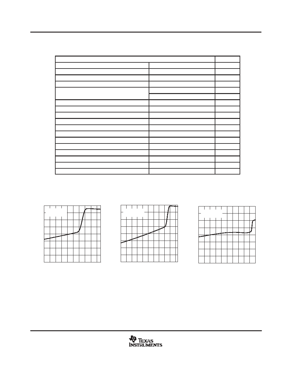
Figure 1
ş2000
ş1500
ş1000
ş500
0
500
1000
1500
2000
0
0.3 0.6 0.9 1.2 1.5 1.8 2.1 2.4 2.7
INPUT OFFSET VOLTAGE
vs
COMMON-MODE INPUT VOLTAGE
ş Input Offset V
oltage ş
V
IO
A
Á
VIC ş Common-Mode Input Voltage ş V
VS = 2.7 V
TA = 25
░
C
Figure 2
ş2000
ş1500
ş1000
ş500
0
500
1000
1500
2000
0
0.5
1
1.5
2 2.5
3 3.5
4
4.5
5
INPUT OFFSET VOLTAGE
vs
COMMON-MODE INPUT VOLTAGE
VIC ş Common-Mode Input Voltage ş V
ş Input Offset V
oltage ş
V
IO
A
Á
VS = 5 V
TA = 25
░
C
Figure 3
ş2000
ş1500
ş1000
ş500
0
500
1000
1500
2000
ş0.2
7.5
15.2
INPUT OFFSET VOLTAGE
vs
COMMON-MODE INPUT VOLTAGE
VIC ş Common-Mode Input Voltage ş V
ş Input Offset V
oltage ş
V
IO
A
Á
VS = 15 V
TA = 25
░
C