TLV1572
2.7 V TO 5.5 V, 10-BIT, 1.25 MSPS
SERIAL ANALOG-TO-DIGITAL CONVERTER WITH AUTO-POWERDOWN
SLAS171A DECEMBER 1997 REVISED SEPTEMBER 1998
1
POST OFFICE BOX 655303
·
DALLAS, TEXAS 75265
D
Fast Throughput Rate: 1.25 MSPS
D
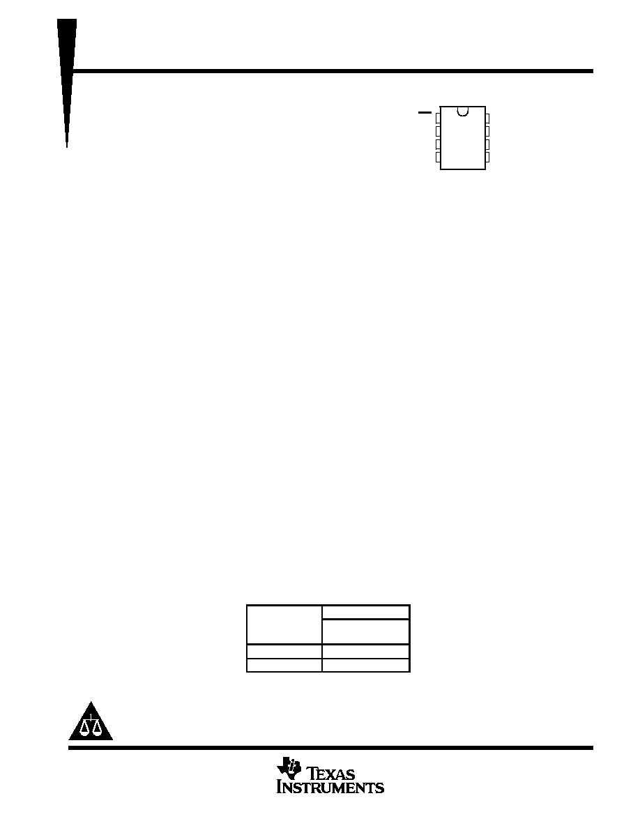
8-Pin SOIC Package
D
Differential Nonlinearity Error: <
±
1 LSB
D
Integral Nonlinearity Error: <
±
1 LSB
D
Signal-to-Noise and Distortion Ratio: 59 dB,
f
(input)
= 500 kHz
D
Single 3-V to 5-V Supply Operation
D
Very Low Power: 8 mW at 3V; 25mW at 5 V
D
Auto-Powerdown: 10
µ
A Maximum
D
Glueless Serial Interface to TMS320 DSPs
and (Q)SPI Compatible Micro-Controllers
D
Inherent Internal Sample and Hold
Operation
Applications
D
Mass Storage and HDD
D
Automotive
D
Digital Servos
D
Process Control
D
General Purpose DSP
D
Contact Image Sensor Processing
description
The TLV1572 is a high-speed 10-bit successive-approximation analog-to-digital converter (ADC) that operates
from a single 2.7-V to 5.5-V power supply and is housed in a small 8-pin SOIC package.
The TLV1572 accepts an analog input range from 0 to V
CC
and digitizes the input at a maximum 1.25 MSPS
throughput rate. The power dissipation is only 8 mW with a 3-V supply or 25 mW with a 5-V supply. The device
features an auto-powerdown mode that automatically powers down to 10
µ
A whenever a conversion is not
performed.
The TLV1572 communicates with digital microprocessors via a simple 3- or 4-wire serial port that interfaces
directly to the Texas Instruments TMS320 DSPs and (Q)SPI compatible microcontrollers without using
additional glue logic.
Very high throughput rate, simple serial interface, SO-8 package, 3-V operation, and low power consumption
make the TLV1572 an ideal choice for compact or remote high-speed systems.
AVAILABLE OPTIONS
PACKAGE
TA
SMALL OUTLINE
(D)
0
°
C to 70
°
C
TLV1572CD
40
°
C to 85
°
C
TLV1572ID
Copyright
©
1998, Texas Instruments Incorporated
PRODUCTION DATA information is current as of publication date.
Products conform to specifications per the terms of Texas Instruments
standard warranty. Production processing does not necessarily include
testing of all parameters.
Please be aware that an important notice concerning availability, standard warranty, and use in critical applications of
Texas Instruments semiconductor products and disclaimers thereto appears at the end of this data sheet.
1
2
3
4
8
7
6
5
CS
VREF
GND
AIN
DO
FS
V
CC
SCLK
D PACKAGE
(TOP VIEW)

TLV1572
2.7 V TO 5.5 V, 10-BIT, 1.25 MSPS
SERIAL ANALOG-TO-DIGITAL CONVERTER WITH AUTO-POWERDOWN
SLAS171A DECEMBER 1997 REVISED SEPTEMBER 1998
2
POST OFFICE BOX 655303
·
DALLAS, TEXAS 75265
functional block diagram
AIN
SCLK
FS
CS
DO
10-BIT
SAR ADC
CONTROL LOGIC
VCC
GND
VREF
GND
VREF
Terminal Functions
TERMINAL
I/O
DESCRIPTION
NAME
NO.
I/O
DESCRIPTION
CS/Powerdown
1
I
Chip Select. A low on this input enables the TLV1572. A high disables the device and disconnects the power
to the TLV1572.
AIN
2
I
Analog input
VREF
3
I
Reference voltage input. The voltage applied to this pin defines the input span of the TLV1572.
GND
4
Ground
DO
5
O
Serial data output. A/D conversion results are provided at this output pin.
FS
6
I
Frame sync input in DSP mode. The falling edge of the frame sync pulse from DSP indicates the start of
a serial data frame shifted out of the TLV1572. The FS input is tied to VCC when interfacing to a
micro-controller.
SCLK
7
I
Serial clock input. This clock synchronizes the serial data transfer and is also used for internal data
conversion.
VCC
8
Power supply, recommend connection to analog supply

TLV1572
2.7 V TO 5.5 V, 10-BIT, 1.25 MSPS
SERIAL ANALOG-TO-DIGITAL CONVERTER WITH AUTO-POWERDOWN
SLAS171A DECEMBER 1997 REVISED SEPTEMBER 1998
3
POST OFFICE BOX 655303
·
DALLAS, TEXAS 75265
absolute maximum ratings over operating free-air temperature (unless otherwise noted)
Supply voltage, GND to V
CC
0.3 V to 6.5 V
. . . . . . . . . . . . . . . . . . . . . . . . . . . . . . . . . . . . . . . . . . . . . . . . . . . . . . .
Analog input voltage range
0.3 V to V
CC
+ 0.3 V
. . . . . . . . . . . . . . . . . . . . . . . . . . . . . . . . . . . . . . . . . . . . . . . . . .
Reference input voltage
V
CC
+ 0.3 V
. . . . . . . . . . . . . . . . . . . . . . . . . . . . . . . . . . . . . . . . . . . . . . . . . . . . . . . . . . . . .
Digital input voltage range
0.3 V to V
CC
+ 0.3 V
. . . . . . . . . . . . . . . . . . . . . . . . . . . . . . . . . . . . . . . . . . . . . . . . . .
Operating
virtual junction temperature range, T
J
40
°
C to 150
°
C
. . . . . . . . . . . . . . . . . . . . . . . . . . . . . . . . . . . .
Operating free-air temperature range, T
A
0
°
C to 70
°
C
. . . . . . . . . . . . . . . . . . . . . . . . . . . . . . . . . . . . . . . . . . . . . .
Storage temperature range, T
stg
65
°
C to 150
°
C
. . . . . . . . . . . . . . . . . . . . . . . . . . . . . . . . . . . . . . . . . . . . . . . . . . .
Lead temperature 1.6 mm (1/16 inch) from case for 10 seconds
260
°
C
. . . . . . . . . . . . . . . . . . . . . . . . . . . . . . .
Stresses beyond those listed under "absolute maximum ratings" may cause permanent damage to the device. These are stress ratings only, and
functional operation of the device at these or any other conditions beyond those indicated under "recommended operating conditions" is not
implied. Exposure to absolute-maximum-rated conditions for extended periods may affect device reliability.
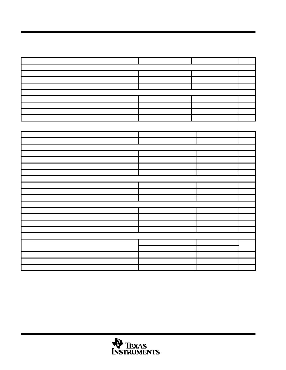
recommended operating conditions
power supply
MIN
NOM
MAX
UNIT
VCC
Supply voltage
2.7
5.5
V
analog inputs
MIN
MAX
UNIT
VAIN
Analog input voltage
GND
VREF
V
VREF
Reference input voltage
2.7
VCC
V
digital inputs
MIN
NOM
MAX
UNIT
High-level input voltage, VIH
VCC = 3 V to 5.5 V
2.1
2.4
V
Low-level input voltage, VIL
VCC = 3 V to 5.5 V
0.8
V
Input SCLK frequency
VCC = 4.5 V to 5.5 V
20
MHZ
SCLK pulse duration, clock high, tw(SCLKH)
VCC = 4.5 V to 5.5 V
23
ns
SCLK pulse duration, clock low, tw(SCLKL)
VCC = 4.5 V to 5.5 V
23
ns
Input SCLK frequency
VCC = 3 V
10
MHZ
SCLK pulse duration, clock high, tw(SCLKH)
VCC = 3 V
45
ns
SCLK pulse duration, clock low, tw(SCLKL)
VCC = 3 V
45
ns
TLV1572
2.7 V TO 5.5 V, 10-BIT, 1.25 MSPS
SERIAL ANALOG-TO-DIGITAL CONVERTER WITH AUTO-POWERDOWN
SLAS171A DECEMBER 1997 REVISED SEPTEMBER 1998
4
POST OFFICE BOX 655303
·
DALLAS, TEXAS 75265
electrical characteristics over recommended operating free-air temperature range, V
CC
= 5 V,
V
REF
= 5 V, f
SCLK
= 20 MHz (unless otherwise noted)
digital specifications
PARAMETER
TEST CONDITIONS
MIN
TYP
MAX
UNIT
Logic inputs
IIH
High-level input current
VCC = 5 V
50
50
µ
A
IIL
Low-level input current
VCC = 5 V
50
50
µ
A
Ci
input capacitance
5
pF
Logic outputs
VOH
High-level output voltage
IOH = 50
µ
A 0.5 mA
VCC 0.4
V
VOL
Low-level output voltage
IOL = 50
µ
A 0.5 mA
0.4
V
IOZ
High-impedance-state output current
50
50
µ
A
CO
Output capacitance
5
pF
dc specifications
PARAMETER
TEST CONDITIONS
MIN
TYP
MAX
UNIT
Resolution
10
Bits
Accuracy
INL
Integral nonlinearity
Best fit
±
0.5
±
1
LSB
DNL
Differential nonlinearity
±
0.3
±
1
LSB
Offset error
±
0.1
±
0.15
%FSR
Gain error
±
0.1
±
0.2
%FSR
Analog input
Input full scale range
GND
VCC
V
Input capacitance
15
pF
input leakage current
VAIN = 0 to VCC
50
µ
A
Voltage reference input
VREF+
Positive reference voltage
3
VCC
V
VREF
Negative reference voltage
Internally connects to GND
GND
V
Input resistance
2
K
Input capcitance
300
pF
Power supply
ICC + IREF Operating supply current
VCC = 5.5 V, fSCLK = 20 MHz
5.5
8.5
mA
ICC + IREF Operating supply current
VCC = 3 V,
fSCLK = 10 MHz
2.7
mA
IPD
Supply current in powerdown mode
VCC
10
µ
A
Power dissipation
VCC = 5 V
25
mW
Power dissipation
VCC = 3 V
8
mW

TLV1572
2.7 V TO 5.5 V, 10-BIT, 1.25 MSPS
SERIAL ANALOG-TO-DIGITAL CONVERTER WITH AUTO-POWERDOWN
SLAS171A DECEMBER 1997 REVISED SEPTEMBER 1998
5
POST OFFICE BOX 655303
·
DALLAS, TEXAS 75265
electrical characteristics over recommended operating free-air temperature range, V
CC
= 5 V,
V
REF
= 5 V, f
SCLK
= 20 MHz (unless otherwise noted) (continued)
ac specifications
PARAMETER
TEST CONDITIONS
MIN
TYP
MAX
UNIT
Signal-to-noise ratio + distortion
f(input) = 200 kHz
54
58
dB
THD
Total harmonic distortion
f(input) = 200 kHz
56
60
dB
Effective number of bits
f(input) = 200 kHz
8.7
9.35
Bits
Spurious-free dynamic range
f(input) = 200 kHz
57
62
dB
Analog Input
BW
Full-power bandwidth
Source impedance = 1 k
12
MHz
BW
Small-signal bandwidth
Source impedance = 1 k
20
Mhz
timing specifications
PARAMETER
TEST CONDITIONS
MIN
TYP
MAX
UNIT
tc
SCLK period
VCC = 4.5 V 5.5 V
50
ns
tc
SCLK period
VCC = 2.7 V 3.3 V
100
ns
trs
Reset and sampling period
6
SLCK
cycles
tc
Conversion period
10
SLCK
cycles
tsu1
FS setup time to SCLK falling edge in DSP mode
10
ns
th1
FS hold time to SCLK falling edge in DSP mode
4
ns
tsu2
FS setup time to CS falling edge in DSP mode
6
ns
th2
FS hold time to CS falling edge in DSP mode
9
ns
td1
Output delay after SCLK rising edge in DSP mode
15
25
ns
td(L)1
FS falling edge to next SCLK falling edge in DSP mode
6
ns
td(L)2
SCLK rising edge after CS falling edge in
µ
C mode
4
ns
td2
Output delay after SCLK rising edge in
µ
C mode
15
25
ns
Specifications subject to change without notice.