
TLV1570
2.7 V TO 5.5 V 8-CHANNEL 10-BIT 1.25-MSPS
SERIAL ANALOG-TO-DIGITAL CONVERTER
SLAS169A DECEMBER 1997 REVISED SEPTEMBER 1998
1
POST OFFICE BOX 655303
·
DALLAS, TEXAS 75265
D
Fast Throughput Rate: 1.25 MSPS at 5 V,
625 KSPS at 3 V
D
Wide Analog Channel Input: 0 V to AV
DD
D
Eight Analog Input Channels
D
Channel Auto-Scan
D
Differential Nonlinearity Error: <
±
1 LSB
D
Integral Nonlinearity Error: <
±
1 LSB
D
Signal-to-Noise and Distortion Ratio: 57 dB
D
Single 2.7-V to 5.5-V Supply Operation
D
Very Low Power: 40 mW at 5.5 V,
8 mW at 2.7 V
D
Auto-Power Down: 300
µ
A Max
D
Software Power Down: 10
µ
A Max
D
Glueless Serial Interface to TMS320 DSPs
and (Q)SPI Compatible Microcontrollers
D
Programmable Internal Reference Voltage:
3.8-V Reference for 5-V Operation,
2.3-V Reference for 3-V Operation
applications
D
Mass Storage and Hard Disk Drive
D
Automotive
D
Digital Servos
D
Process Control
D
General Purpose DSP
D
Image Sensor Processing
description
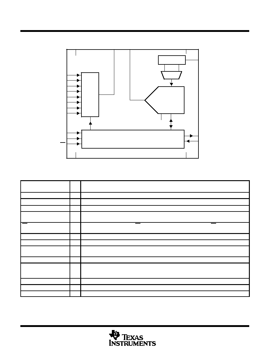
The TLV1570 is a 10-bit data acquisition system that combines an 8-channel input multiplexer (MUX), a
high-speed 10-bit ADC, an on-chip reference, and a high-speed serial interface. The device contains an on-chip
control register allowing control of channel selection, conversion start, reference voltage levels, and power
down via the serial port. The MUX is independently accessible, which allows the user to insert a signal
conditioning circuit such as an anti-aliasing filter or an amplifier, if required, between the MUX and the ADC.
Therefore one signal conditioning circuit can be used for all eight channels.
The TLV1570 operates from a single 2.7-V to 5.5-V power supply. The device accepts an analog input range
from 0 V to AV
DD
and digitizes the input at a maximum 1.25 MSPS throughput rate. Power dissipation is only
8 mW with a 2.7-V supply or 40 mW with a 5.5-V supply. The device features an auto-power down mode that
automatically powers down to 300
µ
A, 10 ns after a conversion is performed. With software power down
enabled, the device is further powered down to only 10
µ
A.
The TLV1570 communicates with digital microprocessors via a simple 4- or 5-wire serial port that interfaces
directly to Texas Instruments TMS320 DSPs, and SPI
TM
and QSPI
TM
compatible microcontrollers without using
additional glue logic.
A very high throughput rate, a simple serial interface, and low power consumption make the TLV1570 an ideal
choice for high-speed digital signal processing requiring multiple analog inputs.
AVAILABLE OPTIONS
PACKAGED DEVICES
TA
SMALL OUTLINE
(DW)
SMALL OUTLINE
(PW)
0
°
C to 70
°
C
TLV1570CDW
TLV1570CPW
40
°
C to 85
°
C
TLV1570IDW
TLV1570IPW
SPI and QSPI are trademarks of Motorola, Inc.
Copyright
©
1998, Texas Instruments Incorporated
PRODUCTION DATA information is current as of publication date.
Products conform to specifications per the terms of Texas Instruments
standard warranty. Production processing does not necessarily include
testing of all parameters.
Please be aware that an important notice concerning availability, standard warranty, and use in critical applications of
Texas Instruments semiconductor products and disclaimers thereto appears at the end of this data sheet.
1
2
3
4
5
6
7
8
9
10
20
19
18
17
16
15
14
13
12
11
CH4
CH3
CH2
CH1
CH0
DV
DD
DGND
FS
SCLK
SDIN
AIN
MO
CH5
CH6
CH7
AV
DD
AGND
REF
CS
SDOUT
DW OR PW PACKAGE
(TOP VIEW)
TLV1570
2.7 V TO 5.5 V 8-CHANNEL 10-BIT 1.25-MSPS
SERIAL ANALOG-TO-DIGITAL CONVERTER
SLAS169A DECEMBER 1997 REVISED SEPTEMBER 1998
2
POST OFFICE BOX 655303
·
DALLAS, TEXAS 75265
functional block diagram
CH0
CH1
CH2
CH3
CH4
CH5
CH6
CH7
SCLK
SDIN
CS
SDOUT
FS
MUX
REFERENCE
10-BIT
SAR ADC
I/O REGISTERS
AND CONTROL LOGIC
AVDD
DVDD
AGND
DGND
MO
AIN
REF
AGND
REF+
REF
Terminal Functions
TERMINAL
I/O
DESCRIPTION
NAME
NO.
I/O
DESCRIPTION
AGND
14
Analog ground
AIN
20
I
ADC analog input
AVDD
15
Analog supply voltage, 2.7 V to 5.5 V
CH0 CH7
5,4,3,2,1,
18,17,16
I
Analog input channels 0 7
CS
12
I
Chip Select. A low level signal on CS enables the TLV1570. A high level signal on CS disables the device
and disconnects power to the TLV1570.
DGND
7
Digital ground
DVDD
6
Digital supply voltage, 2.7 V to 5.5 V
FS
8
I
Frame sync. The falling edge of the frame sync pulse from a DSP indicates the start of a serial data frame
shifted out of the TLV1570. FS is pulled high when interfaced to a microcontroller.
MO
19
O
On-chip MUX analog output
REF
13
I
Reference voltage input. The voltage applied to REF defines the input span of the TLV1570. In external
reference mode, a 0.1
µ
F decoupling capacitor must be placed between the reference and AGND. This
is not required for internal reference mode.
SCLK
9
I
Serial clock input. SCLK synchronizes the serial data transfer and is also used for internal data conversion.
SDIN
10
I
Serial data input used to configure the internal control register.
SDOUT
11
O
Serial data output. A/D conversion results are output at SDOUT.
TLV1570
2.7 V TO 5.5 V 8-CHANNEL 10-BIT 1.25-MSPS
SERIAL ANALOG-TO-DIGITAL CONVERTER
SLAS169A DECEMBER 1997 REVISED SEPTEMBER 1998
3
POST OFFICE BOX 655303
·
DALLAS, TEXAS 75265
detailed description
analog-to-digital converter
The TLV1570 ADC uses the SAR architecture described in this section. The CMOS threshold detector in the
successive-approximation conversion system determines the value of each bit by examining the charge on a
series of binary-weighted capacitors (see Figure 1). In the first phase of the conversion process, the analog input
is sampled by closing the S
C
switch and all S
T
switches simultaneously. This action charges all of the capacitors
to the input voltage.
SC
Threshold
Detector
Node 512
REF
REF+
ST
512
VI
To Output
Latches
REF
ST
REF+
REF
ST
REF+
REF
ST
REF+
REF
ST
REF+
ST
REF+
REF
ST
REF+
REF
ST
1
1
2
4
8
128
256
REF
NOTE: REF is tied to AGND
Figure 1. Simplified Model of the Successive-Approximation System
In the next phase of the conversion process, all S
T
and S
C
switches are opened and the threshold detector
begins identifying bits by identifying the charge (voltage) on each capacitor relative to the reference (REF)
voltage (REF is tied to AGND). In the switching sequence, ten capacitors are examined separately until all ten
bits are identified and then the charge-convert sequence is repeated. In the first step of the conversion phase,
the threshold detector looks at the first capacitor (weight = 512). Node 512 of this capacitor is switched to the
REF+ voltage, and the equivalent nodes of all the other capacitors on the ladder are switched to REF. If the
voltage at the summing node is greater than the trip point of the threshold detector (approximately one-half V
CC
),
a bit 0 is placed in the output register and the 512-weight capacitor is switched to REF. If the voltage at the
summing node is less than the trip point of the threshold detector, a bit 1 is placed in the register and the
512-weight capacitor remains connected to REF+ through the remainder of the successive-approximation
process. The process is repeated for the 256-weight capacitor, the 128-weight capacitor, and so forth down the
line until all bits are counted.
With each step of the successive-approximation process, the initial charge is redistributed among the
capacitors. The conversion process relies on charge redistribution to count and weigh the bits from MSB to LSB.
In the case of the TLV1570, REF is tied to ground and REF+ is connected to the REF input.
The TLV1570 can be programmed to use the on-chip internal reference (DI6=1). The user can select between
two values of internal reference, 2.3 V or 3.8 V, using the control bit DI5.
During internal reference mode, the reference voltage is not output on the REF pin. Therefore it cannot be
decoupled to analog ground (AGND), which acts as the negative reference for the ADC, using an external
capacitor. Hence this mode requires the ground noise to be very low. The REF pin can be left open in this mode.

TLV1570
2.7 V TO 5.5 V 8-CHANNEL 10-BIT 1.25-MSPS
SERIAL ANALOG-TO-DIGITAL CONVERTER
SLAS169A DECEMBER 1997 REVISED SEPTEMBER 1998
4
POST OFFICE BOX 655303
·
DALLAS, TEXAS 75265
sampling frequency, f
s
The TLV1570 requires 16 SCLKs for each sampling and conversion, therefore the equivalent maximum
sampling frequency achievable with a given SCLK frequency is:
f
s(MAX)
= (1/16)f
SCLK
power down
The TLV1570 offers two different power-down options. With auto power-down mode enabled, (DI4=0) the ADC
proceeds to power down if FS is not detected on the 17th falling SCLK edge of a cycle (a cycle starts with FS
being detected on a falling edge of SCLK) in DSP mode and after 16 SCLKs in
µ
C mode. The TLV1570 will
recover from auto power down when FS goes high in DSP mode or when the next SCLK comes in
µ
C mode.
In the case of software power down, the ADC goes to the software power-down state one cycle after CR.DI15
is set to 1. Unlike auto power down which recovers in 1 SCLK, software power down takes 16 SCLKs to recover.
DESCRIPTION
AUTO POWER DOWN
SOFTWARE
POWERDOWN
CS = DVDD
Maximum power down dissipation current
300
µ
A
10
µ
A
Comparator
Power down
Powerdown
Clock buffer
Power down
Powerdown
Reference
Active
Powerdown
Register
Not saved
Not saved
Minimum power down time
1 SCLK
1
µ
s
Minimum resume time
1 SCLK
800 ns
Power down
DSP mode
No FS present one SCLK after previous conversion completed
CR.DI15 set to 1
Power down
Microprocessor mode (FS = 1)
SCLK stopped after previous conversion completed
CR.DI15 set to 1
Power up
DSP mode
FS present
CR.DI15 set to 1
Power up
Microprocessor mode (FS = 1)
SCLK present
CR.DI15 set to 1
Only in DSP mode is input buffer of clock in power-down mode.
The software power down enable/disable bit is not acted until the start of the next cycle (see section configuring the TLV1570 for more information.
configuring the TLV1570
The TLV1570 is to be configured by writing the control bits to SDIN. The configuration will not take affect until
the next cycle. A new configuration is needed for each conversion. Once the channel input and other options
are selected, the conversion takes place in the next cycle. Conversion results are shifted out as conversion
progresses ( see Figure 2).
17
32
One Cycle
Second Cycle
ts
tconv
ts
tconv
Result 0
Result 1
Configure Data 1
Configure Data 2
SCLK
SDOUT
SDIN
Figure 2. TLV1570 Configuration Cycle Timing
TLV1570
2.7 V TO 5.5 V 8-CHANNEL 10-BIT 1.25-MSPS
SERIAL ANALOG-TO-DIGITAL CONVERTER
SLAS169A DECEMBER 1997 REVISED SEPTEMBER 1998
5
POST OFFICE BOX 655303
·
DALLAS, TEXAS 75265
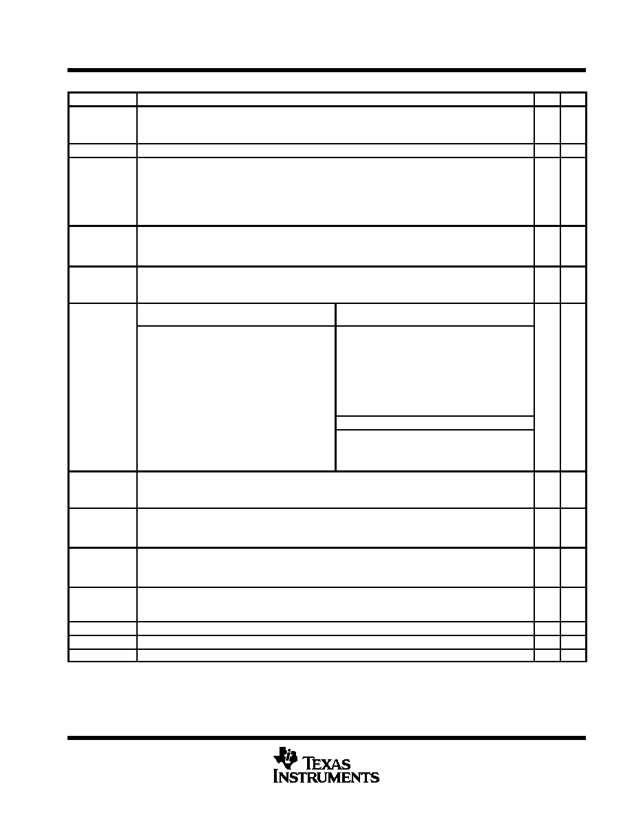
configuration register (CR) definition
BIT
DESCRIPTION
5 V
3 V
Software power down:
X
X
DI15
0:
1:
Normal
Power down enabled
X
X
DI14
Reads out values of the internal register, 1 read. Only DI15 DI1 are read out.
X
X
These two bits select the self-test voltage to be applied to the ADC input during next clock cycle:
X
X
00:
Allow AIN to come in normally
DI13, DI12
01:
Apply AGND to AIN
10:
Apply VREF/2 to AIN
11:
N/A
Choose speed application
X
X
DI11
0:
High speed (higher power consumption)
1:
Low speed (lower power consumption)
This bit enables channel auto-scan function.
X
X
DI10
0:
1:
Auto-scan disabled
Auto-scan enabled
DI9 DI7 These three bits select which of the eight
channels is to be used (if DI10 = 0).
DI9, DI8 These two bits select the channel swept
sequence used by auto scan mode (if DI10 = 1)
X
X
000:
Channel 0 selected as input
00:
Analog inputs CH0, CH1, CH2,
...
.., CH7
sequentially selected
001:
Channel 1 selected as input
01:
Analog inputs CH1, CH3, CH5, CH7
sequentially selected
DI9, DI8, DI7
010:
Channel 2 selected as input
10:
Analog inputs CH0, CH2, CH4, CH6
sequentially selected
011:
Channel 3 selected as input
11:
Analog inputs CH7, CH6, CH5,
...
.., CH0
sequentially selected
100:
Channel 4 selected as input
DI7 Auto-scan reset
101:
Channel 5 selected as input
0:
No reset
110:
Channel 6 selected as input
1:
Reset autoscan sequence
111:
Channel 7 selected as input
Selects Internal or external reference voltage:
X
X
DI6
0:
1:
External
Internal
Selects internal reference voltage value to be applied to the ADC during next conversion cycle.
DI5
0:
2.3 V
X
1:
3.8 V
X
Enables/disables auto-power down function:
X
X
DI4
1:
Enable
0:
Disable
DI3
Performance optimizer linearity
0: AVDD = 5.5 V to 3.6 V
1: AVDD = 3.5 V to 2.7 V
X
X
DI2
Always write 0 (reserved bit)
X
X
DI1
Always write 0 (reserved bit)
X
X
DI0
Always write 0 (reserved bit)
X
X