
TLV0831C, TLV0831I
TLV0832C, TLV0832I
3-VOLT 8-BIT ANALOG-TO-DIGITAL CONVERTERS WITH SERIAL CONTROL
SLAS148 SEPTEMBER 1996
1
POST OFFICE BOX 655303
·
DALLAS, TEXAS 75265
D
8-Bit Resolution
D
2.7 V to 3.6 V V
CC
D
Easy Microprocessor Interface or
Standalone Operation
D
Operates Ratiometrically or With V
CC
Reference
D
Single Channel or Multiplexed Twin
Channels With Single-Ended or Differential
Input Options
D
Input Range 0 V to V
CC
With V
CC
Reference
D
Inputs and Outputs Are Compatible With
TTL and MOS
D
Conversion Time of 32
µ
s at
f
(CLK)
= 250 kHz
D
Designed to Be Functionally Equivalent to
the National Semiconductor ADC0831 and
ADC0832 at 3 V Supply
D
Total Unadjusted Error . . .
±
1 LSB
description
These devices are 8-bit successive-approximation analog-to-digital converters. The TLV0831 has single input
channels; the TLV0832 has multiplexed twin input channels. The serial output is configured to interface with
standard shift registers or microprocessors.
The TLV0832 multiplexer is software configured for single-ended or differential inputs. The differential analog
voltage input allows for common-mode rejection or offset of the analog zero input voltage value. In addition, the
voltage reference input can be adjusted to allow encoding any smaller analog voltage span to the full 8 bits of
resolution.
The operation of the TLV0831 and TLV0832 devices is very similar to the more complex TLV0834 and TLV0838
devices. Ratiometric conversion can be attained by setting the REF input equal to the maximum analog input
signal value, which gives the highest possible conversion resolution. Typically, REF is set equal to V
CC
(done
internally on the TLV0832).
The TLV0831C and TLV0832C are characterized for operation from 0
°
C to 70
°
C. The TLV0831I and TLV0832I
are characterized for operation from 40
°
C to 85
°
C.
AVAILABLE OPTIONS
PACKAGE
TA
SMALL OUTLINE
(D)
PLASTIC DIP
(P)
0
°
C to 70
°
C
TLV0831CD
TLV0832CD
TLV0831CP
TLV0832CP
40
°
C to 85
°
C
TLV0831ID
TLV0832ID
TLV0831IP
TLV0832IP
Please be aware that an important notice concerning availability, standard warranty, and use in critical applications of
Texas Instruments semiconductor products and disclaimers thereto appears at the end of this data sheet.
1
2
3
4
8
7
6
5
CS
IN+
IN
GND
V
CC
CLK
DO
REF
TLV0831 . . . D OR P PACKAGE
(TOP VIEW)
1
2
3
4
8
7
6
5
CS
CH0
CH1
GND
V
CC
/REF
CLK
DO
DI
TLV0832 . . . D OR P PACKAGE
(TOP VIEW)
PRODUCTION DATA information is current as of publication date.
Products conform to specifications per the terms of Texas Instruments
standard warranty. Production processing does not necessarily include
testing of all parameters.
Copyright
©
1996, Texas Instruments Incorporated
TLV0831C, TLV0831I
TLV0832C, TLV0832I
3-VOLT 8-BIT ANALOG-TO-DIGITAL CONVERTERS WITH SERIAL CONTROL
SLAS148 SEPTEMBER 1996
2
POST OFFICE BOX 655303
·
DALLAS, TEXAS 75265
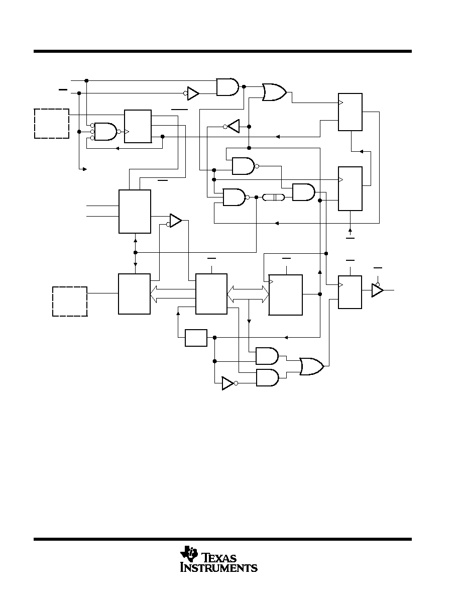
functional block diagram
R
Start
Flip-Flop
S
CLK
CLK
Time
Delay
S
R
CS
DO
CS
CS
D
CLK
R
EOC
9-Bit
Shift
Register
CS
R
CLK
First
LSB
Bit 1
Bits 07
First
One
Shot
SAR
Logic
and
Latch
R
EN
CS
Bits 07
REF
Ladder
and
Decoder
EN
Comparator
EN
Analog
MUX
CH1/IN
CH0/IN+
SGL/DIF
ODD/EVEN
Start
CLK
D
Shift Register
To Internal
Circuits
(TLV0832
only)
DI
CS
CLK
MSB
(TLV0831
only)

TLV0831C, TLV0831I
TLV0832C, TLV0832I
3-VOLT 8-BIT ANALOG-TO-DIGITAL CONVERTERS WITH SERIAL CONTROL
SLAS148 SEPTEMBER 1996
3
POST OFFICE BOX 655303
·
DALLAS, TEXAS 75265
functional description
The TLV0831 and TLV0832 use a sample-data-comparator structure that converts differential analog inputs by
a successive-approximation routine. The input voltage to be converted is applied to an input terminal and is
compared to ground (single ended), or to an adjacent input (differential). The TLV0832 input terminals can be
assigned a positive (+) or negative () polarity. The TLV0831 contains only one differential input channel with
fixed polarity assignment; therefore it does not require addressing. The signal can be applied differentially,
between IN+ and IN, to the TLV0831 or can be applied to IN+ with IN grounded as a single ended input. When
the signal input applied to the assigned positive terminal is less than the signal on the negative terminal, the
converter output is all zeros.
Channel selection and input configuration are under software control using a serial-data link from the controlling
processor. A serial-communication format allows more functions to be included in a converter package with no
increase in size. In addition, it eliminates the transmission of low-level analog signals by locating the converter
at the analog sensor and communicating serially with the controlling processor. This process returns noise-free
digital data to the processor.
A conversion is initiated by setting CS low, which enables all logic circuits. CS must be held low for the complete
conversion process. A clock input is then received from the processor. An interval of one clock period is
automatically inserted to allow the selected multiplexed channel to settle. DO comes out of the high-impedance
state and provides a leading low for one clock period of multiplexer settling time. The SAR comparator compares
successive outputs from the resistive ladder with the incoming analog signal. The comparator output indicates
whether the analog input is greater than or less than the resistive-ladder output. As the conversion proceeds,
conversion data is simultaneously output from DO, with the most significant bit (MSB) first. After eight clock
periods, the conversion is complete. When CS goes high, all internal registers are cleared. At this time, the
output circuits go to the high-impedance state. If another conversion is desired, CS must make a high-to-low
transition followed by address information.
A TLV0832 input configuration is assigned during the multiplexer-addressing sequence. The multiplexer
address shifts into the converter through the data input (DI) line. The multiplexer address selects the analog
inputs to be enabled and determines whether the input is single ended or differential. When the input is
differential, the polarity of the channel input is assigned. In addition to selecting the differential mode, the polarity
may also be selected. Either channel of the channel pair may be designated as the negative or positive input.
On each low-to-high transition of the clock input, the data on DI is clocked into the multiplexer-address shift
register. The first logic high on the input is the start bit. A 2-bit assignment word follows the start bit on the
TLV0832. On each successive low-to-high transition of the clock input, the start bit and assignment word are
shifted through the shift register. When the start bit is shifted into the start location of the multiplexer register,
the input channel is selected and conversion starts. The TLV0832 DI terminal to the multiplexer shift register
is disabled for the duration of the conversion.
The TLV0832 outputs the least-significant-bit (LSB) first data after the MSB-first data stream. The DI and DO
terminals can be tied together and controlled by a bidirectional processor I/O bit received on a single wire. This
is possible because DI is only examined during the multiplexer-addressing interval and DO is still in the
high-impedance state.

TLV0831C, TLV0831I
TLV0832C, TLV0832I
3-VOLT 8-BIT ANALOG-TO-DIGITAL CONVERTERS WITH SERIAL CONTROL
SLAS148 SEPTEMBER 1996
4
POST OFFICE BOX 655303
·
DALLAS, TEXAS 75265
sequence of operation
Don't Care
1
7
6
2
0
1
2
6
7
MSB
LSB
LSB-First Data
EVEN
DIF
+Sign Bit
ODD
SGL
Start
Bit
1
7
6
5
2
4
3
MSB
DI
DO
CS
tsu
CLK
21
20
19
18
14
13
12
1
2
3
4
5
6
10
11
TLV0832
Hi-Z
0
LSB
tconv
MSB-First Data
MSB
Hi-Z
DO
MUX
Settling Time
CS
CLK
10
9
8
7
6
5
4
3
2
1
tsu
tconv
TLV0831
Hi-Z
MSB-First Data
TLV0832 MUX-ADDRESS CONTROL LOGIC TABLE
MUX ADDRESS
CHANNEL NUMBER
SGL/DIF
ODD/EVEN
CH0
CH1
L
H
L
H
L
L
H
H
+
+
+
+
MUX
Settling Time
H = high level, L = low level,
or + = terminal polarity for the selected input channel
(TLV0832
only)
TLV0831C, TLV0831I
TLV0832C, TLV0832I
3-VOLT 8-BIT ANALOG-TO-DIGITAL CONVERTERS WITH SERIAL CONTROL
SLAS148 SEPTEMBER 1996
5
POST OFFICE BOX 655303
·
DALLAS, TEXAS 75265
absolute maximum ratings over recommended operating free-air temperature range (unless
otherwise noted)
Supply voltage, V
CC
(see Note 1)
6.5 V
. . . . . . . . . . . . . . . . . . . . . . . . . . . . . . . . . . . . . . . . . . . . . . . . . . . . . . . . . . .
Input voltage range, V
I
: Logic
0.3 V to V
CC
+ 0.3 V
. . . . . . . . . . . . . . . . . . . . . . . . . . . . . . . . . . . . . . . . . . . . . . .
Analog
0.3 V to V
CC
+ 0.3 V
. . . . . . . . . . . . . . . . . . . . . . . . . . . . . . . . . . . . . . . . . . . . . .
Input current, I
I
±
5 mA
. . . . . . . . . . . . . . . . . . . . . . . . . . . . . . . . . . . . . . . . . . . . . . . . . . . . . . . . . . . . . . . . . . . . . . . . . .
Total input current
±
20 mA
. . . . . . . . . . . . . . . . . . . . . . . . . . . . . . . . . . . . . . . . . . . . . . . . . . . . . . . . . . . . . . . . . . . . . . .
Operating free-air temperature range, T
A
: C suffix
0
°
C to 70
°
C
. . . . . . . . . . . . . . . . . . . . . . . . . . . . . . . . . . . . . .
I suffix
40
°
C to 85
°
C
. . . . . . . . . . . . . . . . . . . . . . . . . . . . . . . . . . . . .
Storage temperature range, T
stg
65
°
C to 150
°
C
. . . . . . . . . . . . . . . . . . . . . . . . . . . . . . . . . . . . . . . . . . . . . . . . . . .
Lead temperature 1,6 mm (1/16 inch) from case for 10 seconds: P package
260
°
C
. . . . . . . . . . . . . . . . . . . . .
Stresses beyond those listed under "absolute maximum ratings" may cause permanent damage to the device. These are stress ratings only, and
functional operation of the device at these or any other conditions beyond those indicated under "recommended operating conditions" is not
implied. Exposure to absolute-maximum-rated conditions for extended periods may affect device reliability.
NOTE 1: All voltage values, except differential voltages, are with respect to the network ground terminal.
recommended operating conditions
MIN
NOM
MAX
UNIT
Supply voltage, VCC (see clock operating conditions)
2.7
3.3
3.6
V
High-level input voltage, VIH
2
V
Low-level input voltage, VIL
0.8
V
Clock frequency f(CLK)
VCC = 2.7 V
250
kHz
Clock frequency, f(CLK)
VCC = 3.3 V
10
600
kHz
Clock duty cycle (see Note 2)
40%
60%
Pulse duration, CS high, twH(CS)
220
ns
Setup time, CS low or TLV0832 data valid before CLK
, tsu
350
ns
Hold time, TLV0832 data valid after CLK
, th
90
ns
Operating free air temperature TA
C suffix
0
70
°
C
Operating free-air temperature, TA
I suffix
40
85
°
C
NOTE 2: The clock-duty-cycle range ensures proper operation at all clock frequencies. When a clock frequency is used outside the
recommended duty-cycle range, the minimum pulse duration (high or low) is 1
µ
s.