TLS1233
VIDEO PREAMPLIFIER SYSTEM
SLVS126C JULY 1995 REVISED JUNE 1996
1
POST OFFICE BOX 655303
·
DALLAS, TEXAS 75265
D
Wide Bandwidth . . . Typ 100 MHz at 3 dB
D
Three Channels
D
0 V to 4 V, Digital Level-Contrast Control
D
0 V to 4 V, Digital Level-Gain Adjust Control
D
20-Pin Plastic DIP for Small PCB Area
Required
D
Fewer Peripheral Components Required
Than for LM1203 Applications
D
Independent CLAMP(+) Adjustment to Each
Channel
description
The TLS1233 is a 100-MHz wide-band video preamplifier system intended for mid-to-high-resolution RGB
(red-green-blue) color monitors. Each video amplifier (R, G, and B) contains a gain set for adjusting maximum
system gain (A
V
= 7.8 V/V). The TLS1233 provides digital level-operated contrast, brightness, and gain
adjustment control. All the control inputs offer high input impedance and an operation range from 0 V to 4 V for
easy interface to the serial digital buses. Provided in a 20-pin plastic dual-in-line package (DIP), the TLS1233
integrates most of the external components required to accommodate the video system.
The TLS1233 operates from a 12-V supply and contains an internal input bias voltage. Also, the TLS1233
contains the feedback resistor required between output and CLAMP() for dc level holding. The device is
characterized for operation from 0
°
C to 70
°
C.
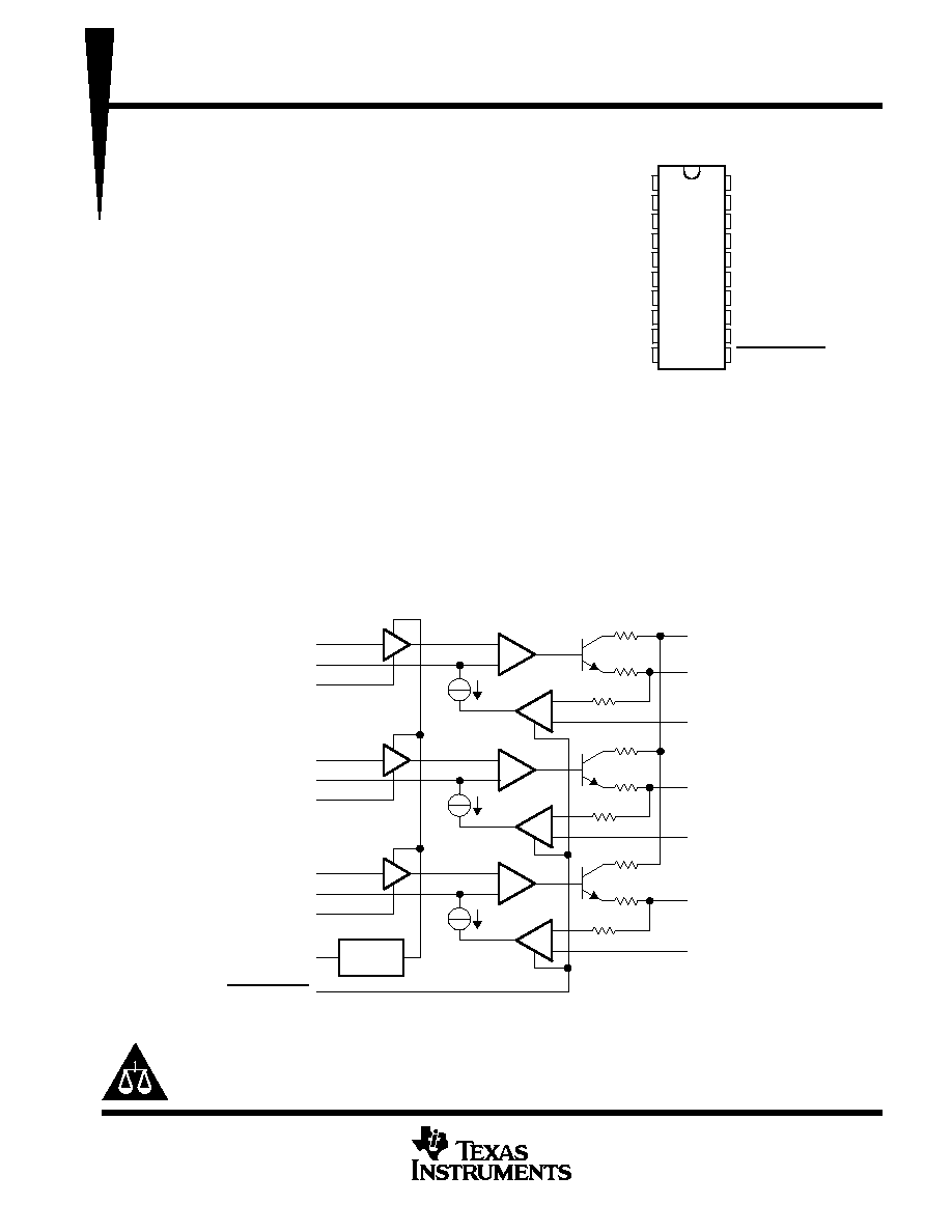
functional block diagram
Contrast
Control
A1
A1
A1
A2
A2
A2
16
18
1
15
20
13
19
VCC2
R VIDEO OUT
R CLAMP(+)
G VIDEO OUT
G CLAMP(+)
B VIDEO OUT
B CLAMP(+)
3
4
17
5
7
14
8
9
12
10
11
R VIDEO IN
R CLAMP CAP
R GAIN ADJUST
G VIDEO IN
G CLAMP CAP
G GAIN ADJUST
B VIDEO IN
B CLAMP CAP
B GAIN ADJUST
CONTRAST
CLAMP GATE
Please be aware that an important notice concerning availability, standard warranty, and use in critical applications of
Texas Instruments semiconductor products and disclaimers thereto appears at the end of this data sheet.
1
2
3
4
5
6
7
8
9
10
20
19
18
17
16
15
14
13
12
11
R CLAMP(+)
V
CC1
R VIDEO IN
R CLAMP CAP
G VIDEO IN
GND
G CLAMP CAP
B VIDEO IN
B CLAMP CAP
CONTRAST
G CLAMP(+)
B CLAMP(+)
R VIDEO OUT
R GAIN ADJUST
V
CC2
G VIDEO OUT
G GAIN ADJUST
B VIDEO OUT
B GAIN ADJUST
CLAMP GATE
N PACKAGE
(TOP VIEW)
PRODUCTION DATA information is current as of publication date.
Products conform to specifications per the terms of Texas Instruments
standard warranty. Production processing does not necessarily include
testing of all parameters.
Copyright
©
1996, Texas Instruments Incorporated
TLS1233
VIDEO PREAMPLIFIER SYSTEM
SLVS126C JULY 1995 REVISED JUNE 1996
2
POST OFFICE BOX 655303
·
DALLAS, TEXAS 75265
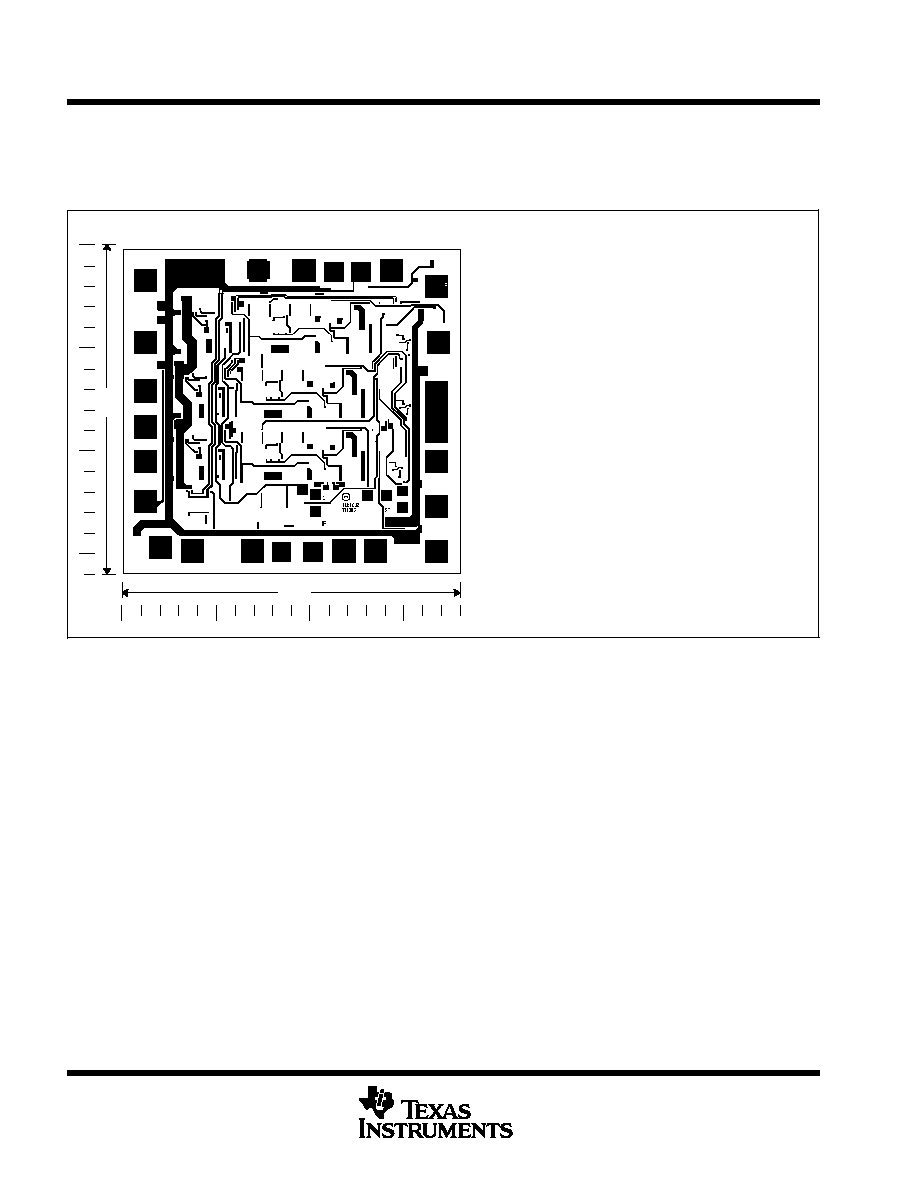
TLS1233Y chip information
This chip, when properly assembled, displays characteristics similar to the TLS1233. Thermal compression or
ultrasonic bonding may be used on the doped-aluminum bonding pads. The chips may be mounted with
conductive epoxy or a gold-silicon preform.
BONDING PAD ASSIGNMENTS
CHIP THICKNESS: 15 TYPICAL
BONDING PADS: 4
×
4 MINIMUM
TJ max = 150
°
C
TOLERANCES ARE
±
10%.
ALL DIMENSIONS ARE IN MILS.
2
1
20
19
18
17
16
15
14
13
12
11
10
9
8
7
6
6
5
4
3
76
78
absolute maximum ratings over operating free-air temperature range (unless otherwise noted)
Supply voltage, V
CC
13.5 V
. . . . . . . . . . . . . . . . . . . . . . . . . . . . . . . . . . . . . . . . . . . . . . . . . . . . . . . . . . . . . . . . . . . . .
Input voltage range, V
I
(see Note 1)
0 V to V
CC
. . . . . . . . . . . . . . . . . . . . . . . . . . . . . . . . . . . . . . . . . . . . . . . . . . . .
Video output current, I
O
(per channel)
28 mA
. . . . . . . . . . . . . . . . . . . . . . . . . . . . . . . . . . . . . . . . . . . . . . . . . . . . . .
Total power dissipation at (or below) 25
°
C free-air temperature (see Note 2)
1.87 W
. . . . . . . . . . . . . . . . . . . .
Operating virtual junction temperature range, T
J
55
°
C to 150
°
C
. . . . . . . . . . . . . . . . . . . . . . . . . . . . . . . . . . . .
Operating free-air temperature range, T
A
0
°
C to 70
°
C
. . . . . . . . . . . . . . . . . . . . . . . . . . . . . . . . . . . . . . . . . . . . . .
Storage temperature range, T
stg
65
°
C to 150
°
C
. . . . . . . . . . . . . . . . . . . . . . . . . . . . . . . . . . . . . . . . . . . . . . . . . .
Lead temperature 1,6 mm (1/16 inch) from case for 10 seconds
260
°
C
. . . . . . . . . . . . . . . . . . . . . . . . . . . . . . .
Stresses beyond those listed under "absolute maximum ratings" may cause permanent damage to the device. These are stress ratings only, and
functional operation of the device at these or any other conditions beyond those indicated under "recommended operating conditions" is not
implied. Exposure to absolute-maximum-rated conditions for extended periods may affect device reliability.
NOTES:
1. All VCC terminals must be externally wired together to prevent internal damage during VCC power-on/-off cycles.
2. For operation above 25
°
C free-air temperature, derate linearly from 1.87 W (TA = 25
°
C) to 1.2 W (TA = 70
°
C). This equates to a
derating factor of 15 mW/
°
C.

TLS1233
VIDEO PREAMPLIFIER SYSTEM
SLVS126C JULY 1995 REVISED JUNE 1996
3
POST OFFICE BOX 655303
·
DALLAS, TEXAS 75265
recommended operating conditions
MIN
NOM
MAX
UNIT
Supply voltage, VCC1 and VCC2
11
12
13
V
High-level input voltage range, CLAMP GATE, VIH
Clamp comparators off
2.4
5
V
Low-level input voltage range, CLAMP GATE, VIL
Clamp comparators on
0
0.8
V
Operating free-air temperature, TA
0
70
°
C
electrical characteristics at 25
°
C free-air temperature range, CLAMP GATE = 0 V, CLAMP(+) = 2 V,
CONTRAST = R,G,B GAIN ADJUST = 4 V, V
CC1
=V
CC2
= 12 V (see Figure 2) (unless otherwise noted)
PARAMETER
ALTERNATE
SYMBOL
TEST CONDITIONS
MIN
TYP
MAX
UNIT
ICC
Supply current
VCC1 + VCC2
84
94
mA
Vref
Video input reference voltage
Measure R/G/B video input
2.1
2.3
2.5
V
II
Contrast and R,G,B GAIN ADJUST
input current
Measure CONTRAST,
R/G/B GAIN ADJUST
0.5
-10
µ
A
IIL
Clamp gate low input current
CLAMP GATE
= 0 V
0.5
2.4
µ
A
IIH
Clamp gate high input current
CLAMP GATE
= 12 V
0.005
1
µ
A
Clamp capacitor charge current
IK(chg)
R,G,B CLAMP CAP = 0 V
1
mA
Clamp capacitor discharge current
IK(dschg)
R,G,B CLAMP CAP = 5 V
1
mA
VOL
Low-level output voltage
R,G,B CLAMP CAP = 0 V
0.3
V
VOH
High-level output voltage
R,G,B CLAMP CAP = 5 V
7.8
V
VO(diff)
Output voltage difference
VO(diff)
Between any two channels
±
0.5
±
50
mV
operating characteristics at 25
°
C free-air temperature, CLAMP GATE = 0 V, CLAMP(+) = 4 V,
CONTRAST = R,G,B GAIN ADJUST = 4 V, f
I
= 10 kHz, V
CC1
= V
CC2
= 12 V (unless otherwise noted)
PARAMETER
ALTERNATE
SYMBOL
TEST CONDITIONS
MIN
TYP
MAX
UNIT
AV(max) Maximum voltage amplification
AVMAX
CONTRAST = 4 V,
VIPP = 700 mV
7.8
V/V
AV(mid)
Midrange voltage amplification
AVMID
CONTRAST = 2 V,
VIPP = 700 mV
2
V/V
Contrast voltage for minimum
amplification
VCONT-LOW
VI(PP) = 1 V,
See Note 3
1
V
Amplification match at AV(max)
AVmax(diff)
CONTRAST = 4 V,
See Note 4
±
0.2
dB
Amplification match at AV(mid)
AVmid(diff)
CONTRAST = 2 V,
See Note 3
±
0.2
dB
Amplification match at AV(low)
AVlow(diff)
CONTRAST = VCONT-LOW,
See Note 3 and 4
±
0.2
dB
THD
Total harmonic distortion
CONTRAST = 1 V,
VIPP = 1 V
0.5
%
BW
Amplifier bandwidth
BW(3 dB)
CONTRAST = 4 V,
See Notes 5 And 7
100
MHz
Crosstalk attenuation
a
CONTRAST = 4 V,
See Note 6
f = 10 kHz,
60
dB
Crosstalk attenuation
ax
CONTRAST = 4 V,
f = 10 MHz,
See Notes 6 or 7
40
dB
Pulse test for rise time
tr
CONTRAST = 4 V,
CLAMP(+) = 2 V,
3
ns
Pulse test for fall time
tf
VO(PP) = 4 V
( )
See Notes 5 and 7
4
ns
NOTES:
3. Determine VCONT-LOW for 40 dB attenuation of output. Reference to AV(max).
4. Measure gain difference between any two amplifiers, VI(PP) = 1 V.
5. Adjust input frequency from 10 kHz (AV(max) reference level) to the 3-dB corner frequency (f 3 dB). VI(PP) = 700 mV.
6. VI(PP) = 700 mV at f = 10 kHz to any amplifier. Measure output levels of the other two undriven amplifiers relative to driven amplifier.
7. A special text fixture without a socket and a double-sided full-ground-plane PC board are required.
TLS1233
VIDEO PREAMPLIFIER SYSTEM
SLVS126C JULY 1995 REVISED JUNE 1996
4
POST OFFICE BOX 655303
·
DALLAS, TEXAS 75265
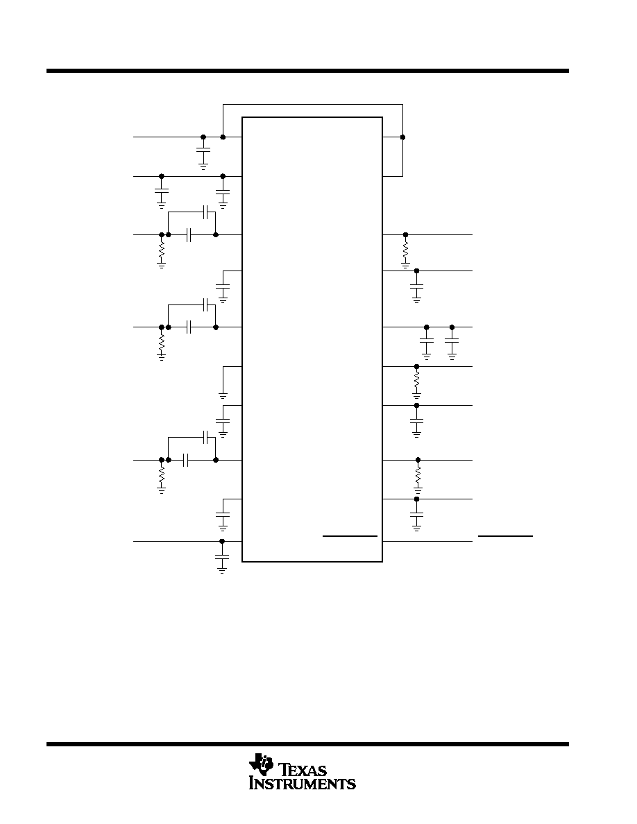
PARAMETER MEASUREMENT INFORMATION
R CLAMP(+)
G CLAMP(+)
0.1
µ
F
VCC1
B CLAMP(+)
0.1
µ
F
10
µ
F
R VIDEO IN
R VIDEO OUT
0.1
µ
F
0.1
µ
F
10
µ
F
75
390
R CLAMP CAP R GAIN ADJUST
0.1
µ
F
G VIDEO IN
VCC2
0.1
µ
F
10
µ
F
75
390
0.1
µ
F
10
µ
F
GND
G VIDEO OUT
0.1
µ
F
G CLAMP CAP G GAIN ADJUST
0.1
µ
F
B VIDEO IN
B VIDEO OUT
0.1
µ
F
10
µ
F
75
390
0.1
µ
F
B CLAMP CAP B GAIN ADJUST
0.1
µ
F
CONTRAST
CLAMP GATE
0.1
µ
F
1
2
3
4
5
6
7
8
9
10
20
19
18
17
16
15
14
13
12
11
To Red
Cascade Driver
0 V to 4 V
12 V
To Green
Cascade Driver
0 V to 4 V
To Blue
Cascade Driver
0 V to 4 V
CLAMP GATE
CLAMP(+)
12 V
R Video In
G Video In
B Video In
CONTRAST
+
+
+
+
+
Figure 1. Test Circuit

TLS1233
VIDEO PREAMPLIFIER SYSTEM
SLVS126C JULY 1995 REVISED JUNE 1996
5
POST OFFICE BOX 655303
·
DALLAS, TEXAS 75265
APPLICATION INFORMATION
R CLAMP (+)
G CLAMP(+)
0.1
µ
F
VCC1
B CLAMP(+)
0.1
µ
F
10
µ
F
R VIDEO IN
R VIDEO OUT
0.1
µ
F
0.1
µ
F
10
µ
F
75
390
R CLAMP CAP R GAIN ADJUST
0.1
µ
F
G VIDEO IN
VCC2
0.1
µ
F
10
µ
F
75
390
0.1
µ
F
10
µ
F
GND
G VIDEO OUT
0.1
µ
F
G CLAMP CAP G GAIN ADJUST
0.1
µ
F
B VIDEO IN
B VIDEO OUT
0.1
µ
F
10
µ
F
75
390
0.1
µ
F
B CLAMP CAP B GAIN ADJUST
0.1
µ
F
CONTRAST
CLAMP GATE
0.1
µ
F
1
2
3
4
5
6
7
8
9
10
20
19
18
17
16
15
14
13
12
11
To Red
Cascade Driver
12 V
To Green
Cascade Driver
To Blue
Cascade Driver
CLAMP GATE
12 V
R Video In
G Video In
B Video In
CONTRAST
4 V
4 V
4 V
4 V
4 V
4 V
4 V
+
+
+
+
+
Minimum pulse width: 300 ns
100
100
Figure 2. Application Circuit