1
2
3
4
5
6
7
8
9
10
11
12
24
23
22
21
20
19
18
17
16
15
14
13
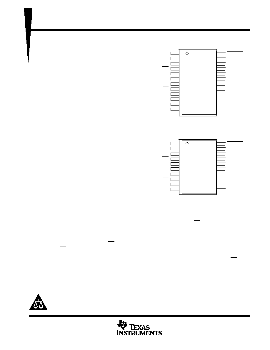
SCLK
FS
SDI
EOC/INT
SDO
DGND
DV
DD
CS
A0
A1
A2
A3
CSTART
AV
DD
AGND
BGAP
REFM
REFP
AGND
AV
DD
A7
A6
A5
A4
TLC3548
DW OR PW PACKAGE
(TOP VIEW)
1
2
3
4
5
6
7
8
9
10
20
19
18
17
16
15
14
13
12
11
SCLK
FS
SDI
EOC/INT
SDO
DGND
DV
DD
CS
A0
A1
CSTART
AV
DD
AGND
BGAP
REFM
REFP
AGND
AV
DD
A3
A2
TLC3544
DW OR PW PACKAGE
(TOP VIEW)
TLC3544, TLC3548
5-V ANALOG, 3-/5-V DIGITAL, 14-BIT, 200-KSPS, 4-/8-CHANNELS SERIAL
ANALOG-TO-DIGITAL CONVERTERS WITH 0-5 V (PSEUDODIFFERENTIAL) INPUTS
SLAS266B ş OCTOBER 2000 ş REVISED AUGUST 2001
1
POST OFFICE BOX 655303
Ě
DALLAS, TEXAS 75265
D
14-Bit Resolution
D
Maximum Throughput 200 KSPS
D
Analog Input Range 0-V to Reference
Voltage
D
Multiple Analog Inputs:
ş 8 Channels for TLC3548
ş 4 Channels for TLC3544
D
Pseudodifferential Analog Inputs
D
SPI/DSP-Compatible Serial Interfaces With
SCLK up to 25 MHz
D
Single 5-V Analog Supply; 3-/5-V Digital
Supply
D
Low Power:
ş 4 mA (Internal Reference: 1.8 mA) for
Normal Operation
ş 20
Á
A in Autopower-Down
D
Built-In 4-V Reference, Conversion Clock
and 8x FIFO
D
Hardware-Controlled and Programmable
Sampling Period
D
Programmable Autochannel Sweep and
Repeat
D
Hardware Default Configuration
D
INL:
▒
1 LSB Max
D
DNL:
▒
1 LSB Max
D
SINAD: 80.8 dB
D
THD: ş95 dB
description
The TLC3544 and TLC3548 are a family of 14-bit resolution high-performance, low-power, CMOS
analog-to-digital converters (ADC). All devices operate from a single 5-V analog power supply and 3-V to 5-V
digital supply. The serial interface consists of four digital inputs [chip select (CS), frame sync (FS), serial
input-output clock (SCLK), serial data input (SDI)], and a 3-state serial data output (SDO). CS (works as SS,
slave select), SDI, SDO, and SCLK form an SPI interface. FS, SDI, SDO, and SCLK form a DSP interface. The
frame sync signal (FS) indicates the start of a serial data frame being transferred. When multiple converters
connect to one serial port of a DSP, CS works as the chip select to allow the host DSP to access the individual
converter. CS can be tied to ground if only one converter is used. FS must be tied to DV
DD
if it is not used (such
as in an SPI interface). When SDI is tied to DV
DD
, the device is set in hardware default mode after power-on,
and no software configuration is required. In the simplest case, only three wires (SDO, SCLK, and CS or FS)
are needed to interface with the host.
Copyright
2001, Texas Instruments Incorporated
PRODUCTION DATA information is current as of publication date.
Products conform to specifications per the terms of Texas Instruments
standard warranty. Production processing does not necessarily include
testing of all parameters.
Please be aware that an important notice concerning availability, standard warranty, and use in critical applications of
Texas Instruments semiconductor products and disclaimers thereto appears at the end of this data sheet.

TLC3544, TLC3548
5-V ANALOG, 3-/5-V DIGITAL, 14-BIT, 200-KSPS, 4-/8-CHANNELS SERIAL
ANALOG-TO-DIGITAL CONVERTERS WITH 0-5 V (PSEUDODIFFERENTIAL) INPUTS
SLAS266B ş OCTOBER 2000 ş REVISED AUGUST 2001
2
POST OFFICE BOX 655303
Ě
DALLAS, TEXAS 75265
description (continued)
In addition to being a high-speed ADC with versatile control capability, these devices have an on-chip analog
multiplexer (MUX) that can select any analog input or one of three self-test voltages. The sample-and-hold
function is automatically started after the fourth SCLK (normal sampling) or can be controlled by CSTART to
extend the sampling period (extended sampling). The normal sampling period can also be programmed as short
sampling (12 SCLKs) or long sampling (44 SCLKs) to accommodate the faster SCLK operation popular among
high-performance signal processors. The TLC3544 and TLC3548 are designed to operate with low power
consumption. The power saving feature is further enhanced with software power-down/ autopower-down
modes and programmable conversion speeds. The conversion clock (internal OSC) is built in. The converter
can also use an external SCLK as the conversion clock for maximum flexibility. The TLC3544 and TLC3548
have a 4-V internal reference. The converters are specified with unipolar input range of 0-V to 5-V when a 5-V
external reference is used.
AVAILABLE OPTIONS
PACKAGED DEVICES
TA
20-TSSOP
(PW)
20-SOIC
(DW)
24-SOIC
(DW)
24-TSSOP
(PW)
0
░
C to 70
░
C
TLC3544CPW
TLC3544CDW
TLC3548CDW
TLC3548CPW
ş 40
░
C to 85
░
C
TLC3544IPW
TLC3544IDW
TLC3548IDW
TLC3548IPW
functional block diagram
Analog
MUX
4-V
Reference
Command
Decode
CMR (4 MSBs)
SAR
ADC
OSC
Conversion
Clock
FIFO
X8
Control
Logic
4-Bit
Counter
SDO
EOC/INT
DVDD AVDD
DGND AGND
CSTART
FS
CS
SCLK
SDI
CFR
REFM
BGAP
REFP
X8
A0
A1
A2
A3
A4
A5
A6
A7
X4
A0
A1
A2
A3
X
X
X
X
TLC3544, TLC3548
5-V ANALOG, 3-/5-V DIGITAL, 14-BIT, 200-KSPS, 4-/8-CHANNELS SERIAL
ANALOG-TO-DIGITAL CONVERTERS WITH 0-5 V (PSEUDODIFFERENTIAL) INPUTS
SLAS266B ş OCTOBER 2000 ş REVISED AUGUST 2001
3
POST OFFICE BOX 655303
Ě
DALLAS, TEXAS 75265
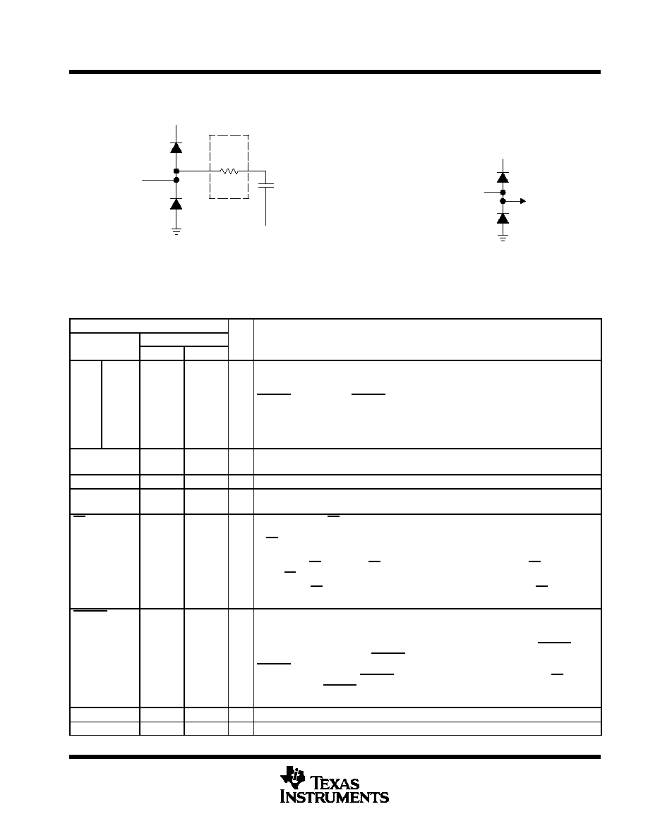
equivalent input circuit
1.1 k
Max
Ron
MUX
C(sample) = 30 pF Max
VDD
REFM
Ain
Diode Turn on Voltage: 35 V
Equivalent Analog Input Circuit
Equivalent Digital Input Circuit
Digital Input
VDD
Terminal Functions
TERMINAL
NAME
NO.
I/O
DESCRIPTION
NAME
TLC3544
TLC3548
I/O
DESCRIPTION
A0
A1
A2
A3
A0
A1
A2
A3
A4
A5
A6
A7
9
10
11
12
9
10
11
12
13
14
15
16
I
Analog signal inputs. Analog input signals applied to these terminals are internally
multiplexed. The driving source impedance should be less than or equal to 1 k
for normal
sampling. For larger source impedance, use the external hardware conversion start signal
CSTART (the low time of CSTART controls the sampling period) or reduce the frequency of
SCLK to increase the sampling time.
AGND
14, 18
18, 22
I
Analog ground return for the internal circuitry. Unless otherwise noted, all analog voltage
measurements are with respect to AGND.
AVDD
13, 19
17, 23
I
Analog supply voltage
BGAP
17
21
I
Internal bandgap compensation pin. Install compensation capacitors between BGAP and
AGND. 0.1
Á
F for external reference; 10
Á
F in parallel with 0.1
Á
F for internal reference.
CS
8
8
I
Chip select. When CS is high, SDO is in high-impedance state, SDI is ignored, and SCLK is
disabled to clock data but works as conversion clock source if programmed. The falling edge
of CS input resets the internal 4-bit counter, enables SDI and SCLK, and removes SDO from
high-impedance state.
If FS is high at CS falling edge, CS falling edge initiates the operation cycle. CS works as slave
select (SS) to provide an SPI interface.
If FS is low at CS falling edge, FS rising edge initiates the operation cycle. CS can be used
as chip select to allow the host to access the individual converter.
CSTART
20
24
I
External sampling trigger signal, which initiates the sampling from a selected analog input
channel when the device works in extended sampling mode (asynchronous sampling). A
high-to-low transition starts the sampling of the analog input signal. A low-to-high transition
puts the S/H in hold mode and starts the conversion. The low time of the CSTART signal
controls the sampling period. CSTART signal must be long enough for proper sampling.
CSTART must stay high long enough after the low-to-high transition for the conversion to finish
maturely. The activation of CSTART is independent of SCLK and the level of CS and FS.
However, the first CSTART cannot be issued before the rising edge of the 11th SCLK. Tie this
terminal to DVDD if not used.
DGND
6
6
I
Digital ground return for the internal circuitry
DVDD
7
7
I
Digital supply voltage

TLC3544, TLC3548
5-V ANALOG, 3-/5-V DIGITAL, 14-BIT, 200-KSPS, 4-/8-CHANNELS SERIAL
ANALOG-TO-DIGITAL CONVERTERS WITH 0-5 V (PSEUDODIFFERENTIAL) INPUTS
SLAS266B ş OCTOBER 2000 ş REVISED AUGUST 2001
4
POST OFFICE BOX 655303
Ě
DALLAS, TEXAS 75265
Terminal Functions (Continued)
TERMINAL
NAME
NO.
I/O
DESCRIPTION
NAME
TLC3544
TLC3548
I/O
DESCRIPTION
EOC(INT)
4
4
O
End of conversion (EOC) or interrupt to host processor (INT)
EOC: used in conversion mode 00 only. EOC goes from high to low at the end of the sampling and
remains low until the conversion is complete and data is ready.
INT: Interrupt to the host processor. The falling edge of INT indicates data is ready for output. INT
is cleared by the following CS
, FS
, or CSTART
.
FS
2
2
I
Frame sync input from DSP. The rising edge of FS indicates the start of a serial data frame being
transferred (coming into or being sent out of the device). If FS is low at the falling edge of CS, the
rising edge of FS initiates the operation cycle, resets the internal 4-bit counter, and enables SDI,
SDO, and SCLK. Tie this pin to DVDD if FS is not used to initiate the operation cycle.
REFM
16
20
I
External low reference input. Connect REFM to AGND.
REFP
15
19
I
External positive reference input. When an external reference is used, the range of maximum input
voltage is determined by the difference between the voltage applied to this terminal and to the
REFM terminal. Always install decoupling capacitors (10
Á
F in parallel with 0.1
Á
F) between REFP
and REFM.
SCLK
1
1
I
Serial clock input from the host processor to clock in the input from SDI and clock out the output
via SDO. It can also be used as the conversion clock source when the external conversion clock
is selected (see Table 2). When CS is low, SCLK is enabled. When CS is high, SCLK is disabled
for the data transfer, but can still work as the conversion clock source.
SDI
3
3
I
Serial data input. The first 4 MSBs, ID[15:12], are decoded as one 4-bit command. All trailing bits,
except for the CONFIGURE WRITE command, are filled with zeros. The CONFIGURE WRITE
command requires additional 12-bit data. The MSB of input data, ID[15], is latched at the first falling
edge of SCLK following FS falling edge, if FS starts the operation, or latched at the falling edge of
first SCLK following CS falling edge when CS initiates the operation.
The remaining input data (if any) is shifted in on the rising edge of SCLK and latched on the falling
edge of SCLK. The input via SDI is ignored after the 4-bit counter counts to 16 (clock edges) or a
low-to-high transition of CS, whichever happens first. Refer to the timing specification for the timing
requirements. Tie SDI to DVDD if using hardware default mode (refer to device initialization).
SDO
5
5
O
The 3-state serial output for the A/D conversion result. All data bits are shifted out through SDO.
SDO is in the high-impedance state when CS is high. SDO is released after a CS falling edge. The
output format is MSB (OD[15]) first.
When FS initiates the operation, the MSB of output via SDO, OD[15], is valid before the first falling
edge of SCLK following the falling edge of FS.
When CS initiates the operation, the MSB, OD[15], is valid before the first falling edge of SCLK
following the CS falling edge.
The remaining data bits are shifted out on the rising edge of SCLK and are valid before the falling
edge of SCLK. Refer to the timing specification for the details.
In a select/conversion operation, the first 14 bits are the results from the previous conversion (data).
In READ FIFO operation,
the data is from FIFO. In both cases, the last two bits are don't care.
In a WRITE operation, the output from SDO is ignored.
SDO goes into high-impedance state at the 16th falling edge of SCLK after the operation cycle is
initiated. SDO is in high-impedance state during conversions in modes 01, 10, and 11.

TLC3544, TLC3548
5-V ANALOG, 3-/5-V DIGITAL, 14-BIT, 200-KSPS, 4-/8-CHANNELS SERIAL
ANALOG-TO-DIGITAL CONVERTERS WITH 0-5 V (PSEUDODIFFERENTIAL) INPUTS
SLAS266B ş OCTOBER 2000 ş REVISED AUGUST 2001
5
POST OFFICE BOX 655303
Ě
DALLAS, TEXAS 75265
absolute maximum ratings over operating free-air temperature (unless otherwise noted)
Supply voltage, GND to AV
DD
, DV
DD
ş0.3 V to 6.5 V
. . . . . . . . . . . . . . . . . . . . . . . . . . . . . . . . . . . . . . . . . . . . . . . .
Analog input voltage range
ş0.2 V to AV
DD
+0.2 V
. . . . . . . . . . . . . . . . . . . . . . . . . . . . . . . . . . . . . . . . . . . . . . . . . .
Analog input current
100 mA MAX
. . . . . . . . . . . . . . . . . . . . . . . . . . . . . . . . . . . . . . . . . . . . . . . . . . . . . . . . . . . . . . . .
Reference input voltage
AV
DD
+ 0.3 V
. . . . . . . . . . . . . . . . . . . . . . . . . . . . . . . . . . . . . . . . . . . . . . . . . . . . . . . . . . . .
Digital input voltage range
ş0.3 V to DV
DD
+ 0.3 V
. . . . . . . . . . . . . . . . . . . . . . . . . . . . . . . . . . . . . . . . . . . . . . . . .
Operating virtual junction temperature range, T
J
ş40
░
C to 150
░
C
. . . . . . . . . . . . . . . . . . . . . . . . . . . . . . . . . . . .
Operating free-air industrial temperature range, T
A
: I suffix
ş40
░
C to 85
░
C
. . . . . . . . . . . . . . . . . . . . . . . . . . . . .
C suffix
0
░
C to 70
░
C
. . . . . . . . . . . . . . . . . . . . . . . . . . . . . .
Storage temperature range, T
stg
ş 65
░
C to 150
░
C
. . . . . . . . . . . . . . . . . . . . . . . . . . . . . . . . . . . . . . . . . . . . . . . . . . .
Lead temperature 1,6 mm (1.16 inch) from case for 10 seconds
260
░
C
. . . . . . . . . . . . . . . . . . . . . . . . . . . . . . .
Stresses beyond those listed under "absolute maximum ratings" may cause permanent damage to the device. These are stress ratings only, and
functional operation of the device at these or any other conditions beyond those indicated under "recommended operating conditions" is not
implied. Exposure to absolute-maximum-rated conditions for extended periods may affect device reliability.