TLC2943
HIGH-PERFORMANCE DUAL PHASE-LOCKED BUILDING BLOCK
SLAS249 NOVEMBER 1999
1
POST OFFICE BOX 655303
·
DALLAS, TEXAS 75265
D
Dual TLC2933 by Multichip Module
(MCM) Technology
D
Voltage-Controlled Oscillators (VCO)
Section
Complete Oscillator Using Only One
External Bias Resistor (RBIAS)
Recommended Lock Frequency
Range
37 MHz to 60 MHz
(V
DD
= 3.3 V
±
0.15 V, T
A
= 20
°
C
to 75
°
C)
43 MHz to 100 MHz
(V
DD
= 5 V
±
0.25 V, T
A
= 20
°
C
to 75
°
C)
D
Includes a High Speed Edge-Triggered
Phase Frequency Detector (PFD) With
Internal Charge Pump
D
Independent VCO, PFD Power
-
Down
Mode
description
The TLC2943 is a multichip module product that
uses two TLC2933 chips. The TLC2933 chip is
composed of a voltage-controlled oscillator (VCO) and an edge-triggered-type phase frequency detector
(PFD). The oscillation frequency range of the VCO is set by an external bias resistor (R
BIAS
). The high-speed
PFD with internal charge pump detects the phase difference between the reference frequency input and signal
frequency input from the external counter. Both the VCO and the PFD have inhibit functions that can be used
as a power-down mode. The high-speed and stable VCO characteristics of the TLC2933 make the TLC2943
suitable for use in dual high-performance phase-locked loop (PLL) systems.
AVAILABLE OPTIONS
TA
PACKAGE
TA
SMALL OUTLINE (DB)
20
°
C to 75
°
C
TLC2943IDB
20
°
C to 75
°
C
TLC2943IDBR (Tape and Reel)
Copyright
©
1999, Texas Instruments Incorporated
PRODUCTION DATA information is current as of publication date.
Products conform to specifications per the terms of Texas Instruments
standard warranty. Production processing does not necessarily include
testing of all parameters.
Please be aware that an important notice concerning availability, standard warranty, and use in critical applications of
Texas Instruments semiconductor products and disclaimers thereto appears at the end of this data sheet.
1
2
3
4
5
6
7
8
9
10
11
12
13
14
15
16
17
18
19
38
37
36
35
34
33
32
31
30
29
28
27
26
25
24
23
22
21
20
LOGIC_1 V
DD
TEST_1
VCO_1 OUT
F
IN
-A_1
F
IN
-B_1
PFD_1 OUT
LOGIC_1 GND
GND
NC
NC
NC
GND
LOGIC_2 V
DD
TEST_2
VCO_2 OUT
F
IN
-A_2
F
IN
-B_2
PFD_2 OUT
LOGIC_2 GND
VCO_1 V
DD
R
BIAS
_1
VCOIN_1
VCO_1 GND
VCO_1 INHIBIT
PFD_1 INHIBIT
NC
GND
NC
NC
NC
GND
VCO_2 V
DD
R
BIAS
_2
VCOIN_2
VCO_2 GND
VCO_2 INHIBIT
PFD_2 INHIBIT
NC
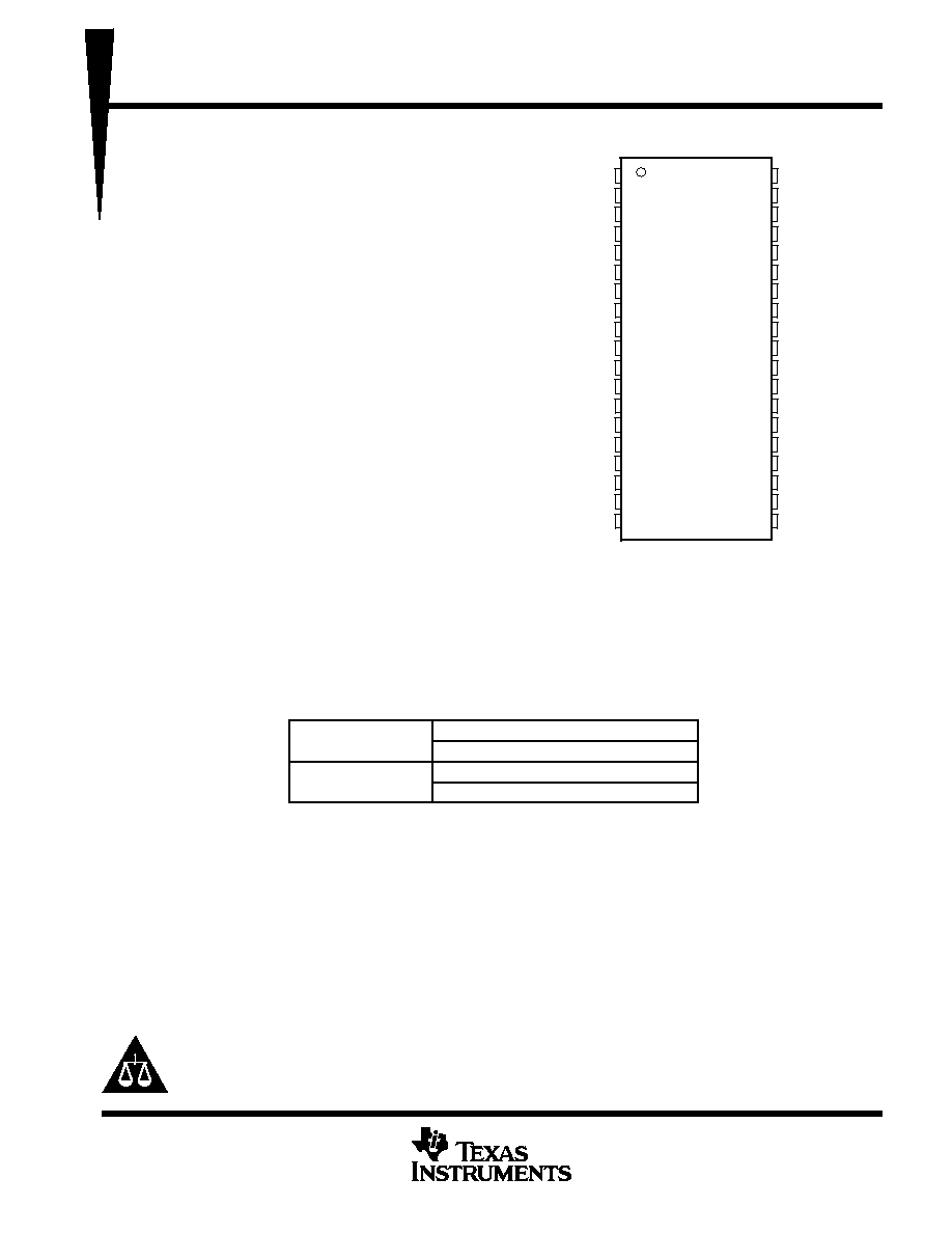
DB PACKAGE
(TOP VIEW)
TLC2943
HIGH-PERFORMANCE DUAL PHASE-LOCKED BUILDING BLOCK
SLAS249 NOVEMBER 1999
2
POST OFFICE BOX 655303
·
DALLAS, TEXAS 75265
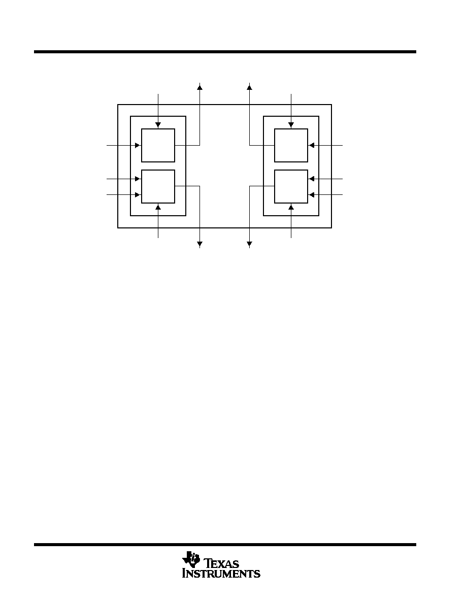
functional block diagram
VCOIN_1
VCO_1
PFD_1
VCO_1 INHIBIT
VCO_1 OUT
FIN-A_1
FIN-B_1
PFD_1 INHIBIT
PFD_1 OUT
VCO_2
PFD_2
VCO_2 OUT
PFD_2 OUT
VCO_2 INHIBIT
PFD_2 INHIBIT
FIN-A_2
FIN-B_2
VCOIN_2
TLC2943
HIGH-PERFORMANCE DUAL PHASE-LOCKED BUILDING BLOCK
SLAS249 NOVEMBER 1999
3
POST OFFICE BOX 655303
·
DALLAS, TEXAS 75265
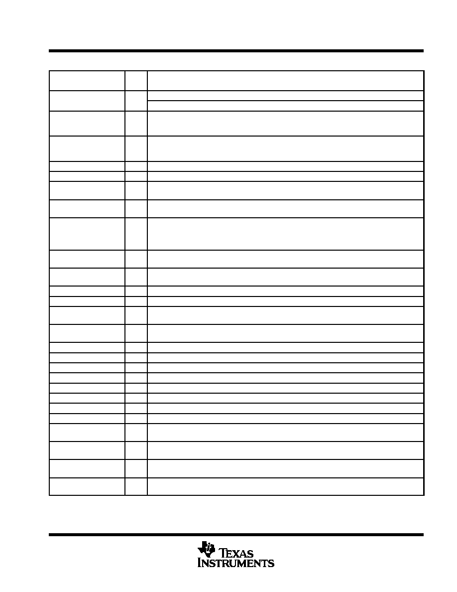
Terminal Functions
TERMINAL
I/O
DESCRIPTION
NAME
NO.
I/O
DESCRIPTION
GND
8, 31
Common GND for chip 1
GND
12, 27
Common GND for chip 2
FINA_1,
FINB_1
4
5
I
Reference frequency signal input and comparison frequency signal input for PFD_1. fREFIN_1 inputs
to FIN-A_1, and comparison frequency input from external counter logic to FINB_1, for a lag-lead filter
use as LPF.
FINA_2,
FINB_2
16
17
I
Reference frequency signal input and comparison frequency signal input for PFD_2. fREFIN_2 inputs
to FIN-A_2, and comparison frequency input from external counter logic to FIN-B_2, for a lag-lead filter use
as LPF.
LOGIC_1 GND
7
Ground for the internal logic of chip 1
LOGIC_2 GND
19
Ground for the internal logic of chip 2
LOGIC_1 VDD
1
Power supply for the internal logic of chip 1. This power supply should be separate from VCO VDD to
reduce cross-coupling between supplies.
LOGIC_2 VDD
13
Power supply for the internal logic of chip 2. This power supply should be separate from VCO VDD to
reduce cross-coupling between supplies.
NC
9, 10,
11, 20,
28, 29,
30, 32
No internal connection
PFD_1 INHIBIT
33
I
PFD inhibit control for chip 1. When PFD_1 INHIBIT is high, PFD_1 OUT is in the high-impedance state,
see Table 2.
PFD_2 INHIBIT
21
I
PFD inhibit control for chip 2. When PFD_2 INHIBIT is high, PFD_2 OUT is in the high-impedance state,
see Table 2.
PFD_1 OUT
6
O
PFD output of chip 1. When the PFD_1 INHIBIT is high, PFD_1 OUT is in the high-impedance state.
PFD_2 OUT
18
O
PFD output of chip 2. When the PFD_2 INHIBIT is high, PFD_2 OUT is in the high-impedance state.
RBIAS_1
37
I
Bias supply for VCO_1. An external resistor (RBIAS) between VCO_1 VDD and BIAS_1 supplies bias for
adjusting the oscillation frequency range of VCO_1.
RBIAS_2
25
I
Bias supply for VCO_2. An external resistor (RBIAS) between VCO_2 VDD and BIAS_2 supplies bias for
adjusting the oscillation frequency range of VCO_2.
TEST_1
2
Test terminal. TEST connects to LOGIC_1 GND for normal operation.
TEST_2
14
Test terminal. TEST connects to LOGIC_2 GND for normal operation.
VCO_1 GND
35
GND for VCO_1
VCO_2 GND
23
GND for VCO_2
VCO_1 INHIBIT
34
I
VCO inhibit control for chip 1. When VCO_1 INHIBIT is high, VCO_1 OUT is low (see Table 1).
VCO_2 INHIBIT
22
I
VCO inhibit control for chip 2. When VCO_2 INHIBIT is high, VCO_2 OUT is low (see Table 1).
VCO_1 OUT
3
O
VCO output of chip 1. When VCO_1 INHIBIT is high, VCO_1 OUT is low.
VCO_2 OUT
15
O
VCO output of chip 2. When VCO_2 INHIBIT is high, VCO_2 OUT is low.
VCO_1 VDD
38
Power supply for VCO_1. This power supply should be separate from LOGIC VDD to reduce
cross-coupling between supplies.
VCO_2 VDD
26
Power supply for VCO_2. This power supply should be separate from LOGIC VDD to reduce
cross-coupling between supplies.
VCOIN_1
36
I
VCO_1 control voltage input. Nominally the external loop filter output connects to VCO IN to control VCO
oscillation frequency.
VCOIN_2
24
I
VCO_2 control voltage input. Nominally the external loop filter output connects to VCO IN to control VCO
oscillation frequency.

TLC2943
HIGH-PERFORMANCE DUAL PHASE-LOCKED BUILDING BLOCK
SLAS249 NOVEMBER 1999
4
POST OFFICE BOX 655303
·
DALLAS, TEXAS 75265
detailed description
MCM (multichip module) technology for TLC2943
The TLC2943 is a multichip module (MCM) product that uses two TLC2933 chips. Inside the package, two chips
are completely isolated by a special formed lead-frame. Therefore,when using the TLC2943 in two
asynchronous PLL circuits, there is no performance degradation by electrical interference between chips inside
the package. So, the same performance as TLC2933 can be easily expected by using TLC2943.
The NC terminals in the middle on both sides of the package are to achieve complete isolation inside the
package. To get the best performance from this MCM technology, it is better to make a careful board layout of
the external power supply, ground, and signal lines.
voltage controlled oscillator (VCO)
VCO_1 and VCO_2 have the same typical characteristics. Each VCO oscillation frequency is determined by
an external resistor (R
BIAS
) connected between the VCO V
DD
and the BIAS terminals. The oscillation frequency
and range depend on this resistor value. The bias resistor value for the minimum temperature coefficient is
nominally 2.2 k
with V
DD
= 3.3 V and nominally 2.4 k
with V
DD
= 5 V. For the lock frequency range, refer to
the recommended operating conditions. Figure 1 shows the typical frequency variation and VCO control
voltage.
BIAS Resistor (RBIAS)
VCO Oscillation Frequency (fosc)
VCO Control Voltage (VCOIN)
VCO Oscillation Frequency Range
Figure 1. VCO_1 and VCO_2 Oscillation Frequency
VCO inhibit function
Each VCO has an externally controlled inhibit function that inhibits the VCO output. The VCO oscillation is
stopped during a high level on VCOINHIBIT, so the high level can also be used as the power-down mode. The
VCO output maintains a low level during the power-down mode (see Table 1 and Table 2).
Table 1. VCO_1 Inhibit Function
VCO_1 INHIBIT
VCO_1 OSCILLATOR
VCO_1 OUT
VCO_1 IDD
Low
Active
Active
Normal
High
Stop
Low
Power down
Table 2. VCO_2 Inhibit Function
VCO_2 INHIBIT
VCO_2 OSCILLATOR
VCO_2 OUT
VCO_2 IDD
Low
Active
Active
Normal
High
Stop
Low
Power down

TLC2943
HIGH-PERFORMANCE DUAL PHASE-LOCKED BUILDING BLOCK
SLAS249 NOVEMBER 1999
5
POST OFFICE BOX 655303
·
DALLAS, TEXAS 75265
detailed description (continued)
phase frequency detector (PFD)
The PFD is a high-speed, edge-triggered detector with an internal charge pump. The PFD detects the phase
difference between two frequency inputs supplied to F
IN
-A and F
IN
-B as shown in Figure 2. Nominally the
reference is supplied to F
IN
-A, and the frequency from the external counter output is fed to F
IN
-B. For clock
recovery PLL systems, other types of phase detectors should be used.
FIN-A_1, 2
FIN-B_1, 2
PFD_1, 2 OUT
VOH
HI-Z
VOL
Figure 2. PFD Function Timing Chart
PFD output control
A high level on PFD INHIBIT places the PFD OUT in the high impedance state and the PFD stops phase
detection as shown in Table 3 and Table 4. A high level on PFD inhibit also can be used as the power-down mode
for the PFD.
Table 3. PFD_1 Inhibit Function
PFD_1 INHIBIT
PFD_1
PFD_1 OUT
PFD_1 IDD
Low
Active
Active
Normal
High
Stop
Hi-Z
Power down
Table 4. PFD_2 Inhibit Function
PFD_2 INHIBIT
PFD_2
PFD_2 OUT
PFD_2 IDD
Low
Active
Active
Normal
High
Stop
Hi-Z
Power down