TL7726
HEX CLAMPING CIRCUITS
SLAS078C SEPTEMBER 1993 REVISED JULY 1999
1
POST OFFICE BOX 655303
·
DALLAS, TEXAS 75265
D
Protects Against Latch-Up
D
25-mA Current Sink in Active State
D
Less Than 1-mW Dissipation in Standby
Condition
D
Ideal for Applications in Environments
Where Large Transient Spikes Occur
D
Stable Operation for All Values of
Capacitive Load
D
No Output Overshoot
description
The TL7726 consists of six identical clamping circuits that monitor an input voltage with respect to a reference
value, REF. For an input voltage (V
I
) in the range of GND to < REF, the clamping circuits present a very high
impedance to ground, drawing current of less than 10
µ
A. The clamping circuits are active for V
I
< GND or
V
I
> REF when they have a very low impedance and can sink up to 25 mA.
These characteristics make the TL7726 ideal as protection devices for CMOS semiconductor devices in
environments where there are large positive or negative transients to protect analog-to-digital converters in
automotive or industrial systems. The use of clamping circuits provides a safeguard against potential latch-up.
The TL7726C is characterized for operation over the temperature range of 0
°
C to 70
°
C. The TL7726I is
characterized for operation over the temperature range of 40
°
C to 85
°
C. The TL7726Q is characterized for
operation over the temperature range of 40
°
C to 125
°
C.
AVAILABLE OPTIONS
TA
SOIC (D)
PLASTIC DIP (P)
0
°
C to 70
°
C
TL7726CD
TL7726CP
40
°
C to 85
°
C
TL7726ID
TL7726IP
40
°
C to 125
°
C
TL7726QD
TL7726QP
The D package is available taped and reeled. Add the suffix R to the
device type (i.e., TL7726CDR).
Please be aware that an important notice concerning availability, standard warranty, and use in critical applications of
Texas Instruments semiconductor products and disclaimers thereto appears at the end of this data sheet.
Copyright
©
1999, Texas Instruments Incorporated
PRODUCTION DATA information is current as of publication date.
Products conform to specifications per the terms of Texas Instruments
standard warranty. Production processing does not necessarily include
testing of all parameters.
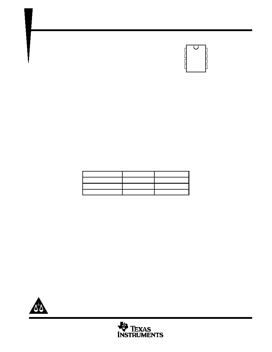
1
2
3
4
8
7
6
5
GND
CLAMP
CLAMP
CLAMP
REF
CLAMP
CLAMP
CLAMP
D OR P PACKAGE
(TOP VIEW)
TL7726
HEX CLAMPING CIRCUITS
SLAS078C SEPTEMBER 1993 REVISED JULY 1999
2
POST OFFICE BOX 655303
·
DALLAS, TEXAS 75265
absolute maximum ratings over operating free-air temperature (unless otherwise noted)
Reference voltage, V
ref
6 V
. . . . . . . . . . . . . . . . . . . . . . . . . . . . . . . . . . . . . . . . . . . . . . . . . . . . . . . . . . . . . . . . . . . . . .
Clamping current, I
IK
±
50 mA
. . . . . . . . . . . . . . . . . . . . . . . . . . . . . . . . . . . . . . . . . . . . . . . . . . . . . . . . . . . . . . . . . . . .
Junction temperature, T
J
150
°
C
. . . . . . . . . . . . . . . . . . . . . . . . . . . . . . . . . . . . . . . . . . . . . . . . . . . . . . . . . . . . . . . . . .
Package thermal impedance,
JA
(see Notes 1 and 2): D package
97
°
C/W
. . . . . . . . . . . . . . . . . . . . . . . . . . . .
P package
127
°
C/W
. . . . . . . . . . . . . . . . . . . . . . . . . . . .
Lead temperature 1,6 mm (1/16 inch) from case for 10 seconds
260
°
C
. . . . . . . . . . . . . . . . . . . . . . . . . . . . . . .
Storage temperature range, T
stg
65
°
C to 150
°
C
. . . . . . . . . . . . . . . . . . . . . . . . . . . . . . . . . . . . . . . . . . . . . . . . . . .
Stresses beyond those listed under "absolute maximum ratings" may cause permanent damage to the device. These are stress ratings only, and
functional operation of the device at these or any other conditions beyond those indicated under "recommended operating conditions" is not
implied. Exposure to absolute-maximum-rated conditions for extended periods may affect device reliability.
NOTES:
1. Maximum power dissipation is a function of TJ(max),
JA, and TA. The maximum allowable power dissipation at any allowable
ambient temperature is PD = (TJ(max) TA)/
JA. Operating at the absolute maximum TJ of 150
°
C can impact reliability.
2. The package thermal impedance is calculated in accordance with JESD 51, except for through-hole packages, which use a trace
length of zero.
recommended operating conditions
MIN
MAX
UNIT
Reference voltage, Vref
4.5
5.5
V
Input clamping current IIK
VI
Vref
25
mA
Input clamping current, IIK
VI
GND
25
mA
TL7726C
0
70
Operating free-air temperature range, TA
TL7726I
40
85
°
C
TL7726Q
40
125
electrical characteristics over recommended operating free-air temperature range (unless
otherwise noted)
PARAMETER
TEST CONDITIONS
MIN
TYP
MAX
UNIT
VIK +
Positive clamp voltage
II = 20 mA
Vref
Vref + 200
mV
VIK
Negative clamp voltage
II = 20 mA
200
0
mV
IZ
Reference current
Vref = 5 V
25
60
µ
A
Vref 50 mV
VI
Vref
10
II
Input current
GND
VI
50 mV
10
µ
A
50 mV
VI
Vref 50 mV
1
1
All typical values are at TA = 25
°
C.
switching characteristics specified at T
A
= 25
°
C
PARAMETER
TEST CONDITIONS
MIN
MAX
UNIT
t
Settling time
VI(system) =
±
13 V,
RI = 600
,
tt < 1
µ
s,
30
µ
s
ts
Settling time
I(system)
,
Measured at 10% to 90%,
I
,
See Figure 1
t
µ
,
30
µ
s

TL7726
HEX CLAMPING CIRCUITS
SLAS078C SEPTEMBER 1993 REVISED JULY 1999
3
POST OFFICE BOX 655303
·
DALLAS, TEXAS 75265
PARAMETER MEASUREMENT INFORMATION
13 V
13 V
0 V
90%
10%
VI(system)
tt
VIK +
95%
5%
ts
VIK
600
VCC = 5 V
TL7726
REF
CLAMP
GND
VI(system)
VIK
TEST CIRCUIT
INPUT WAVEFORM
CLAMP WAVEFORM
tt
ts
Figure 1. Switching Characteristics
II
100 mA
10 mA
1 mA
100
µ
A
10
µ
A
1
µ
A
Vref 50 mV
50 mV
25 mA
VIK
VI
II
25 mA
GND
Vref
VI
1
µ
A
10
µ
A
100
µ
A
1 mA
10 mA
100 mA
VIK+
Figure 2. Tolerance Band for Clamping Circuit
TL7726
HEX CLAMPING CIRCUITS
SLAS078C SEPTEMBER 1993 REVISED JULY 1999
4
POST OFFICE BOX 655303
·
DALLAS, TEXAS 75265
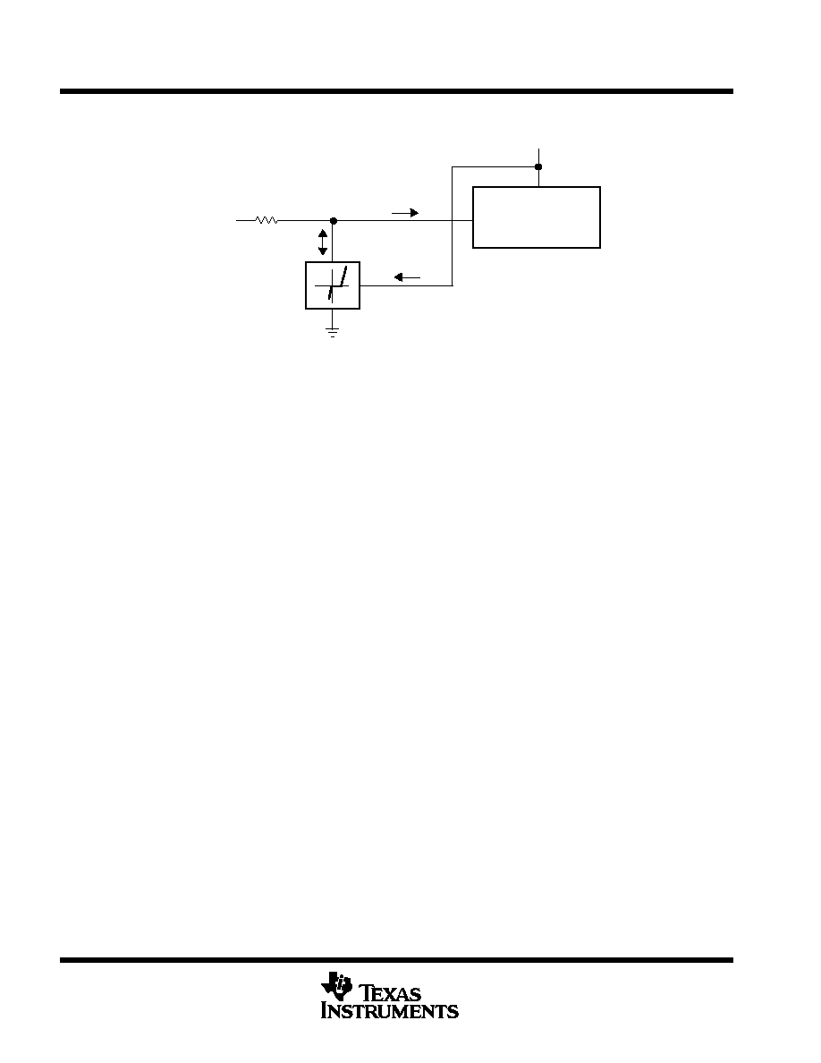
APPLICATION INFORMATION
Device to Be
Protected, e.g.,
A/D Converter,
Microprocessor, etc.
VCC = 5 V
10 k
II
VI
IZ
Vref
1/6
TL7726
VI(system)
(input signal)
II(system)
Example: If II >> II(system), i.e., VI(system)
>
Vref + 200 mV
where:
II(system) = Input current to the device being protected
VI(system) = Input voltage to the device being protected
then the maximum input voltage
VI(system)max = Vref + IImax(10k
)
= 5 V + 25 mA(10k
)
= 5 V + 250 V
= 255 V
Figure 3. Typical Application

IMPORTANT NOTICE
Texas Instruments and its subsidiaries (TI) reserve the right to make changes to their products or to discontinue
any product or service without notice, and advise customers to obtain the latest version of relevant information
to verify, before placing orders, that information being relied on is current and complete. All products are sold
subject to the terms and conditions of sale supplied at the time of order acknowledgement, including those
pertaining to warranty, patent infringement, and limitation of liability.
TI warrants performance of its semiconductor products to the specifications applicable at the time of sale in
accordance with TI's standard warranty. Testing and other quality control techniques are utilized to the extent
TI deems necessary to support this warranty. Specific testing of all parameters of each device is not necessarily
performed, except those mandated by government requirements.
CERTAIN APPLICATIONS USING SEMICONDUCTOR PRODUCTS MAY INVOLVE POTENTIAL RISKS OF
DEATH, PERSONAL INJURY, OR SEVERE PROPERTY OR ENVIRONMENTAL DAMAGE ("CRITICAL
APPLICATIONS"). TI SEMICONDUCTOR PRODUCTS ARE NOT DESIGNED, AUTHORIZED, OR
WARRANTED TO BE SUITABLE FOR USE IN LIFE-SUPPORT DEVICES OR SYSTEMS OR OTHER
CRITICAL APPLICATIONS. INCLUSION OF TI PRODUCTS IN SUCH APPLICATIONS IS UNDERSTOOD TO
BE FULLY AT THE CUSTOMER'S RISK.
In order to minimize risks associated with the customer's applications, adequate design and operating
safeguards must be provided by the customer to minimize inherent or procedural hazards.
TI assumes no liability for applications assistance or customer product design. TI does not warrant or represent
that any license, either express or implied, is granted under any patent right, copyright, mask work right, or other
intellectual property right of TI covering or relating to any combination, machine, or process in which such
semiconductor products or services might be or are used. TI's publication of information regarding any third
party's products or services does not constitute TI's approval, warranty or endorsement thereof.
Copyright
©
1999, Texas Instruments Incorporated