TL7700
SUPPLY-VOLTAGE SUPERVISOR
SLVS220A Ù JULY 1999 Ù REVISED NOVEMBER 1999
1
POST OFFICE BOX 655303
ñ
DALLAS, TEXAS 75265
D
Adjustable Sense Voltage With Two
External Resistors
D
Adjustable Hysteresis of Sense Voltage
D
Wide Operating Supply-Voltage
Range . . . 1.8 V to 40 V
D
Wide Operating-Temperature
Range . . . Ù40
¯
C to 85
¯
C
D
Low Power Consumption (I
CC
= 0.6 mA
TYP, V
CC
= 40 V)
D
Minimum External Components
D
Package Options Include Plastic
Small-Outline (PS) and Thin Shrink
Small-Outline (PW) Packages and Standard
DIP (P)
description
The TL7700 is a bipolar integrated circuit designed for use as a reset controller in microcomputer and
microprocessor systems. The SENSE voltage can be set to any value greater than 0.5 V using two external
resistors. The hysteresis value of the sense voltage also can be set by the same resistors. The device includes
a precision voltage reference, fast comparator, timing generator, and output driver, so it can generate a
power-on reset signal in a digital system.
The TL7700 has an internal 1.5-V temperature-compensated voltage reference from which all function blocks
are supplied. Circuit function is very stable, with supply voltage in the 1.8-V to 40-V range. Minimum supply
current allows use with ac line operation, portable battery operation, and automotive applications.
The TL7700C is characterized for operation from Ù40
¯
C to 85
¯
C.
AVAILABLE OPTIONS
PACKAGED DEVICES
TA
PLASTIC
DIP
(P)
PLASTIC
SMALL OUTLINE
(PS)
PLASTIC
THIN SHRINK
SMALL OUTLINE
(PW)
Ù40
¯
C to 85
¯
C
TL7700CP
TL7700CPS
TL7700CPW
PS and PW packages are available taped and reeled. Add the suffix R to device type
(e.g., TL7700CPSR).
Copyright
ˋ
1999, Texas Instruments Incorporated
PRODUCTION DATA information is current as of publication date.
Products conform to specifications per the terms of Texas Instruments
standard warranty. Production processing does not necessarily include
testing of all parameters.
Please be aware that an important notice concerning availability, standard warranty, and use in critical applications of
Texas Instruments semiconductor products and disclaimers thereto appears at the end of this data sheet.
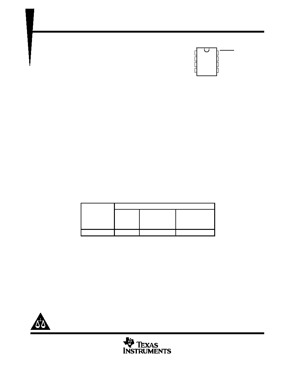
1
2
3
4
8
7
6
5
CT
SENSE
NC
GND
RESET
NC
NC
V
CC
P, PS, OR PW PACKAGE
(TOP VIEW)
NC Ù No internal connection

TL7700
SUPPLY-VOLTAGE SUPERVISOR
SLVS220A Ù JULY 1999 Ù REVISED NOVEMBER 1999
2
POST OFFICE BOX 655303
ñ
DALLAS, TEXAS 75265
functional block diagram
Reference
Voltage
+
Ù
+
Ù
R
S
Q
+
Ù
Vs = 500 mV TYP
RESET
GND
CT
SENSE
ICT = 15
ç
A TYP; Is = 2.5
ç
A TYP
VCC
ICT
High:
On
IS
Terminal Functions
TERMINAL
DESCRIPTION
NAME
NO.
DESCRIPTION
CT
1
Timing capacitor connection. This terminal sets the RESET output pulse duration (tpo). It is connected internally to a
15-
ç
A constant-current source. There is a limit on the switching speed of internal elements; even if CT is set to 0,
response speeds remain at approximately 5 to 10
ç
s. If CT is open, the device can be used as an adjustable-threshold
noninverting comparator. If CT is low, the internal output-stage comparator is active and the RESET output transistor
is on. An external voltage must not be applied to this terminal due to the internal structure of the device. Therefore, drive
the device using an open-collector transistor, FET, or 3-state buffer (in the low-level or high-impedance state).
GND
4
Ground. Keep this terminal as low impedance to reduce circuit noise.
NC
3, 6, 7
No internal connection
RESET
8
Reset output. This terminal can be connected directly to a system that resets in the active-low state. A pullup resistor
usually is required because the output is an npn open-collector transistor. An additional transistor should be connected
when the active-high reset or higher output current is required.
SENSE
2
Voltage sense. This terminal has a threshold level of 500 mV. The sense voltage and hysteresis can be set at the same
time when the two voltage-dividing resistors are connected. The reference voltage is temperature compensated to inhibit
temperature drift in the threshold voltage within the operating temperature range.
VCC
5
Power supply. This terminal is used in an operating-voltage range of 1.8 V to 40 V.
TL7700
SUPPLY-VOLTAGE SUPERVISOR
SLVS220A Ù JULY 1999 Ù REVISED NOVEMBER 1999
3
POST OFFICE BOX 655303
ñ
DALLAS, TEXAS 75265
absolute maximum ratings over operating free-air temperature range (unless otherwise noted)
Supply voltage, V
CC
(see Note 1)
41 V
. . . . . . . . . . . . . . . . . . . . . . . . . . . . . . . . . . . . . . . . . . . . . . . . . . . . . . . . . . . .
Sense input voltage range, V
s
Ù0.3 V to 41 V
. . . . . . . . . . . . . . . . . . . . . . . . . . . . . . . . . . . . . . . . . . . . . . . . . . . . . .
Output voltage, V
OH
(off state)
41 V
. . . . . . . . . . . . . . . . . . . . . . . . . . . . . . . . . . . . . . . . . . . . . . . . . . . . . . . . . . . . . .
Output current, I
OL
(on state)
5 mA
. . . . . . . . . . . . . . . . . . . . . . . . . . . . . . . . . . . . . . . . . . . . . . . . . . . . . . . . . . . . . . .
Package thermal impedance,
JA
(see Notes 2 and 3): P package
85
¯
C/W
. . . . . . . . . . . . . . . . . . . . . . . . . . . .
PS package
95
¯
C/W
. . . . . . . . . . . . . . . . . . . . . . . . . . .
PW package
149
¯
C/W
. . . . . . . . . . . . . . . . . . . . . . . . .
Storage temperature range, T
stg
Ù65
¯
C to 150
¯
C
. . . . . . . . . . . . . . . . . . . . . . . . . . . . . . . . . . . . . . . . . . . . . . . . . . .
Stresses beyond those listed under "absolute maximum ratings" may cause permanent damage to the device. These are stress ratings only, and
functional operation of the device at these or any other conditions beyond those indicated under "recommended operating conditions" is not
implied. Exposure to absolute-maximum-rated conditions for extended periods may affect device reliability.
NOTES:
1. All voltage values are with respect to the network ground terminal.
2. Maximum power dissipation is a function of TJ(max),
JA, and TA. The maximum allowable power dissipation at any allowable
ambient temperature is PD = (TJ(max) Ù TA)/
JA. Operating at the absolute maximum TJ of 150
¯
C can impact reliability.
3. The package thermal impedance is calculated in accordance with JESD 51.
recommended operating conditions
MIN
NOM
MAX
UNIT
Supply voltage, VCC
1.8
40
V
Low-level output current, IOL
3
mA
Operating free-air temperature, TA
Ù40
85
¯
C
electrical characteristics, V
CC
= 3 V, T
A
= 25
¯
C (unless otherwise noted)
PARAMETER
TEST CONDITIONS
MIN
TYP
MAX
UNIT
V
SENSE input voltage
495
500
505
mV
Vs
SENSE input voltage
TA = Ù40
¯
C to 85
¯
C
490
510
mV
I
SENSE input current
V = 0 4 V
2
2.5
3
ç
A
Is
SENSE input current
Vs = 0.4 V
TA = Ù40
¯
C to 85
¯
C
1.5
3.5
ç
A
ICC
Supply current
VCC = 40 V,
Vs = 0.6 V,
No load
0.6
1
mA
VOL
Low level output voltage
IOL = 1.5 mA
0.4
V
VOL
Low-level output voltage
IOL = 3 mA
0.8
V
IOH
High-level output current
VOH = 40 V,
Vs = 0.6 V,
TA = Ù40
¯
C to 85
¯
C
1
ç
A
ICT
Timing-capacitor charge current
Vs = 0.6 V
11
15
19
ç
A
switching characteristics, V
CC
= 3 V, T
A
= 25
¯
C (unless otherwise noted)
PARAMETER
TEST CONDITIONS
MIN
TYP
MAX
UNIT
tpi
SENSE pulse duration
CT = 0.01
ç
F
2
ç
s
tpo
Output pulse duration
CT = 0.01
ç
F
0.5
1
1.5
ms
tr
Output rise time
CT = 0.01
ç
F,
RL = 2.2 k
,
CL = 100 pF
15
ç
s
tf
Output fall time
CT = 0.01
ç
F,
RL = 2.2 k
,
CL = 100 pF
0.5
ç
s
tpd
Propagation delay time, SENSE to output
CT = 0.01
ç
F
10
ç
s

TL7700
SUPPLY-VOLTAGE SUPERVISOR
SLVS220A Ù JULY 1999 Ù REVISED NOVEMBER 1999
4
POST OFFICE BOX 655303
ñ
DALLAS, TEXAS 75265
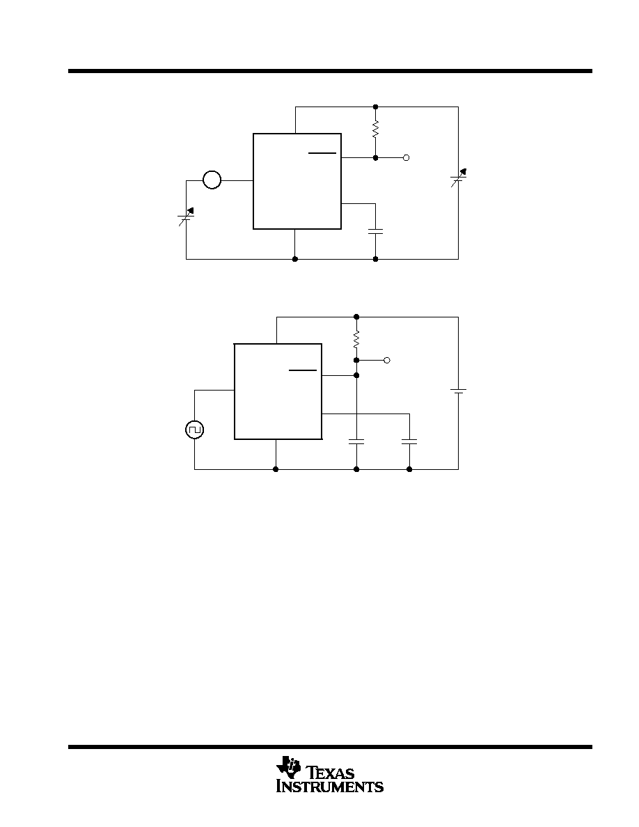
PARAMETER MEASUREMENT INFORMATION
VCC
VCC
Vs
GND
0.6 V
SENSE
A
+
Ù
Figure 1. V
CC
vs I
CC
Measurement Circuit
VCC
VCC
Vs
GND
0.6 V
CT
SENSE
A
+
Ù
Figure 2. V
CC
vs I
CT
0.4 V
VCC
Vs
GND
3 V
CT
RESET
0.01
ç
F
Test
Point
SENSE
Figure 3. I
OL
vs V
OL
TL7700
SUPPLY-VOLTAGE SUPERVISOR
SLVS220A Ù JULY 1999 Ù REVISED NOVEMBER 1999
5
POST OFFICE BOX 655303
ñ
DALLAS, TEXAS 75265
PARAMETER MEASUREMENT INFORMATION
Vs
VCC
Vs
GND
VCC
CT
RESET
2.2 k
0.01
ç
F
Test
Point
SENSE
A
+
Ù
Figure 4. V
S
, I
S
Characteristics
VCC
Vs
GND
3 V
CT
2.2 k
100 pF
Test
Point
Ct
RESET
SENSE
Figure 5. Switching Characteristics