
TL071, TL071A, TL071B, TL072
TL072A, TL072B, TL074, TL074A, TL074B
LOW NOISE JFET INPUT OPERATIONAL AMPLIFIERS
SLOS080G - SEPTEMBER 1978 - REVISED SEPTEMBER 2003
1
POST OFFICE BOX 655303
·
DALLAS, TEXAS 75265
D
Low Power Consumption
D
Wide Common-Mode and Differential
Voltage Ranges
D
Low Input Bias and Offset Currents
D
Output Short-Circuit Protection
D
Low Total Harmonic Distortion
. . . 0.003% Typ
D
Low Noise
V
n
= 18 nV/
Hz Typ at f = 1 kHz
D
High Input Impedance . . . JFET Input Stage
D
Internal Frequency Compensation
D
Latch-Up-Free Operation
D
High Slew Rate . . . 13 V/
µ
s Typ
D
Common-Mode Input Voltage Range
Includes V
CC+
description/ordering information
The JFET-input operational amplifiers in the TL07_ series are designed as low-noise versions of the
TL08_ series amplifiers, with low input bias and offset currents and fast slew rate. The low harmonic distortion
and low noise make the TL07_ series ideally suited for high-fidelity and audio preamplifier applications. Each
amplifier features JFET inputs (for high input impedance) coupled with bipolar output stages integrated on a
single monolithic chip.
The C-suffix devices are characterized for operation from 0
°
C to 70
°
C. The I-suffix devices are characterized
for operation from -40
°
C to 85
°
C. The M-suffix devices are characterized for operation over the full military
temperature range of -55
°
C to 125
°
C.
Please be aware that an important notice concerning availability, standard warranty, and use in critical applications of
Texas Instruments semiconductor products and disclaimers thereto appears at the end of this data sheet.
Copyright
2003, Texas Instruments Incorporated
PRODUCTION DATA information is current as of publication date.
Products conform to specifications per the terms of Texas Instruments
standard warranty. Production processing does not necessarily include
testing of all parameters.
On products compliant to MIL PRF 38535, all parameters are tested
unless otherwise noted. On all other products, production
processing does not necessarily include testing of all parameters.

TL071, TL071A, TL071B, TL072
TL072A, TL072B, TL074, TL074A, TL074B
LOW NOISE JFET INPUT OPERATIONAL AMPLIFIERS
SLOS080G - SEPTEMBER 1978 - REVISED SEPTEMBER 2003
2
POST OFFICE BOX 655303
·
DALLAS, TEXAS 75265
description/ordering information (continued)
ORDERING INFORMATION
TA
VIOmax
AT 25
°
C
PACKAGE
ORDERABLE
PART NUMBER
TOP-SIDE
MARKING
PDIP (P)
Tube of 50
TL071CP
TL071CP
PDIP (P)
Tube of 50
TL072CP
TL072CP
PDIP (N)
Tube of 25
TL074CN
TL074CN
Tube of 75
TL071CD
TL071C
Reel of 2500
TL071CDR
TL071C
SOIC (D)
Tube of 75
TL072CD
TL072C
SOIC (D)
Reel of 2500
TL072CDR
TL072C
10 mV
Tube of 50
TL074CD
TL074C
10 mV
Reel of 2500
TL074CDR
TL074C
SOP (NS)
Reel of 2000
TL074CNSR
TL074
SOP (PS)
Reel of 2000
TL071CPSR
TL071
SOP (PS)
Reel of 2000
TL072CPSR
T072
Reel of 2000
TL072CPWR
T072
TSSOP (PW)
Tube of 90
TL074CPW
T074
TSSOP (PW)
Reel of 2000
TL074CPWR
T074
PDIP (P)
Tube of 50
TL071ACP
TL071ACP
PDIP (P)
Tube of 50
TL072CP
TL072CP
0
°
C to 70
°
C
PDIP (N)
Tube of 25
TL074ACN
TL074ACN
0
°
C to 70
°
C
Tube of 75
TL071ACD
071AC
Reel of 2500
TL071ACDR
071AC
6 mV
SOIC (D)
Tube of 75
TL072ACD
072AC
6 mV
SOIC (D)
Reel of 2500
TL072ACDR
072AC
Tube of 50
TL074ACD
TL074AC
Reel of 2500
TL074ACDR
TL074AC
SOP (PS)
Reel of 2000
TL072ACPSR
T072A
SOP (NS)
Reel of 2000
TL074ACNSR
TL074A
PDIP (P)
Tube of 50
TL071BCP
TL071BCP
PDIP (P)
Tube of 50
TL072BCP
TL072BCP
PDIP (N)
Tube of 25
TL074BCN
TL074BCN
Tube of 75
TL071BCD
071BC
3 mV
Reel of 2500
TL071BCDR
071BC
3 mV
SOIC (D)
Tube of 75
TL072BCD
072BC
SOIC (D)
Reel of 2500
TL072BCDR
072BC
Tube of 50
TL074BCD
TL074BC
Reel of 2500
TL074BCDR
TL074BC
SOP (NS)
Reel of 2000
TL074BCNSR
TL074B
Package drawings, standard packing quantities, thermal data, symbolization, and PCB design guidelines are available at
www.ti.com/sc/package.

TL071, TL071A, TL071B, TL072
TL072A, TL072B, TL074, TL074A, TL074B
LOW NOISE JFET INPUT OPERATIONAL AMPLIFIERS
SLOS080G - SEPTEMBER 1978 - REVISED SEPTEMBER 2003
3
POST OFFICE BOX 655303
·
DALLAS, TEXAS 75265
description/ordering information (continued)
ORDERING INFORMATION
TA
VIOmax
AT 25
°
C
PACKAGE
ORDERABLE
PART NUMBER
TOP-SIDE
MARKING
PDIP (P)
Tube of 50
TL071IP
TL071IP
PDIP (P)
Tube of 50
TL072IP
TL072IP
PDIP (N)
Tube of 25
TL074IN
TL074IN
Tube of 75
TL071ID
TL071I
-40
°
C to 85
°
C
6 mV
Reel of 2500
TL071IDR
TL071I
-40 C to 85 C
6 mV
SOIC (D)
Tube of 75
TL072ID
TL072I
SOIC (D)
Reel of 2500
TL072IDR
TL072I
Tube of 50
TL074ID
TL074I
Reel of 2500
TL074IDR
TL074I
CDIP (JG)
Tube of 50
TL072MJG
TL072MJG
6 mV
CFP (U)
Tube of 150
TL072MU
TL072MU
-55
°
C to 125
°
C
6 mV
LCCC (FK)
Tube of 55
TL072MFK
TL072MFK
-55
°
C to 125
°
C
CDIP (J)
Tube of 25
TL074MJ
TL074MJ
9 mV
CFP (W)
Tube of 25
TL074MW
TL074MW
9 mV
LCCC (FK)
Tube of 55
TL074MFK
TL074MFK
Package drawings, standard packing quantities, thermal data, symbolization, and PCB design guidelines are available at
www.ti.com/sc/package.

TL071, TL071A, TL071B, TL072
TL072A, TL072B, TL074, TL074A, TL074B
LOW NOISE JFET INPUT OPERATIONAL AMPLIFIERS
SLOS080G - SEPTEMBER 1978 - REVISED SEPTEMBER 2003
4
POST OFFICE BOX 655303
·
DALLAS, TEXAS 75265
NC
2OUT
NC
2IN-
NC
1IN+
NC
V
CC+
NC
2IN+
NC
V
CC+
NC
OUT
NC
3
2
1 20 19
9 10 11 12 13
4
5
6
7
8
18
17
16
15
14
NC
1IN-
NC
1IN+
NC
(TOP VIEW)
NC
1OUT
NC
NC
NC
NC
NC
2IN+
CC-
V
CC+
V
1
2
3
4
5
6
7
14
13
12
11
10
9
8
1OUT
1IN-
1IN+
V
CC+
2IN+
2IN-
2OUT
4OUT
4IN-
4IN+
V
CC-
3IN+
3IN-
3OUT
TL074A, TL074B
D, J, N, NS, OR PW PACKAGE
TL074 . . . D, J, N, NS, PW,
OR W PACKAGE
(TOP VIEW)
NC - No internal connection
3
2
1 20 19
9 10 11 12 13
4
5
6
7
8
18
17
16
15
14
NC
IN-
NC
IN+
NC
TL071
FK PACKAGE
(TOP VIEW)
NC
OFFSET
N1
NC
NC
NC
NC
NC
OFFSET
N2
NC
CC-
V
TL072
FK PACKAGE
3
2
1 20 19
9 10 11 12 13
4
5
6
7
8
18
17
16
15
14
4IN+
NC
V
CC-
NC
3IN+
TL074
FK PACKAGE
(TOP VIEW)
1IN-
1OUT
NC
3IN-
4IN-
2IN-
NC
3OUT
4OUT
2OUT
1
2
3
4
8
7
6
5
OFFSET N1
IN-
IN+
V
CC-
NC
V
CC+
OUT
OFFSET N2
TL071, TL071A, TL071B
D, P, OR PS PACKAGE
(TOP VIEW)
1
2
3
4
8
7
6
5
1OUT
1IN-
1IN+
V
CC-
V
CC+
2OUT
2IN-
2IN+
TL072, TL072A, TL072B
D, JG, P, PS, PW, OR U PACKAGE
(TOP VIEW)
symbols
+
-
+
-
IN+
IN-
OUT
IN+
IN-
OUT
TL072 (each amplifier)
TL074 (each amplifier)
TL071
OFFSET N1
OFFSET N2

TL071, TL071A, TL071B, TL072
TL072A, TL072B, TL074, TL074A, TL074B
LOW NOISE JFET INPUT OPERATIONAL AMPLIFIERS
SLOS080G - SEPTEMBER 1978 - REVISED SEPTEMBER 2003
5
POST OFFICE BOX 655303
·
DALLAS, TEXAS 75265
schematic (each amplifier)
C1
VCC+
IN+
VCC-
1080
ÎÎÎ
1080
IN-
TL071 Only
64
128
64
All component values shown are nominal.
ÁÁÁÁÁ
ÁÁÁÁÁ
OFFSET
N1
ÁÁÁ
ÁÁÁ
OFFSET
N2
OUT
18 pF
COMPONENT COUNT
COMPONENT
TYPE
TL071
TL072
TL074
Resistors
11
22
44
Resistors
Transistors
11
14
22
28
44
56
Transistors
JFET
14
2
28
4
56
6
JFET
Diodes
2
1
4
2
6
4
Diodes
Capacitors
epi-FET
1
1
1
2
2
2
4
4
4
Capacitors
epi-FET
1
1
2
2
4
4
Includes bias and trim circuitry

TL071, TL071A, TL071B, TL072
TL072A, TL072B, TL074, TL074A, TL074B
LOW NOISE JFET INPUT OPERATIONAL AMPLIFIERS
SLOS080G - SEPTEMBER 1978 - REVISED SEPTEMBER 2003
6
POST OFFICE BOX 655303
·
DALLAS, TEXAS 75265
absolute maximum ratings over operating free-air temperature range (unless otherwise noted)
Supply voltage (see Note 1): V
CC+
18 V
. . . . . . . . . . . . . . . . . . . . . . . . . . . . . . . . . . . . . . . . . . . . . . . . . . . . . . . . . .
V
CC-
-18 V
. . . . . . . . . . . . . . . . . . . . . . . . . . . . . . . . . . . . . . . . . . . . . . . . . . . . . . . . .
Differential input voltage, V
ID
(see Note 2)
±
30 V
. . . . . . . . . . . . . . . . . . . . . . . . . . . . . . . . . . . . . . . . . . . . . . . . . . .
Input voltage, V
I
(see Notes 1 and 3)
±
15 V
. . . . . . . . . . . . . . . . . . . . . . . . . . . . . . . . . . . . . . . . . . . . . . . . . . . . . . . .
Duration of output short circuit (see Note 4)
Unlimited
. . . . . . . . . . . . . . . . . . . . . . . . . . . . . . . . . . . . . . . . . . . . . . .
Package thermal impedance,
JA
(see Notes 5 and 6): D package (8 pin)
97
°
C/W
. . . . . . . . . . . . . . . . . . . . . .
D package (14 pin)
86
°
C/W
. . . . . . . . . . . . . . . . . . . . .
N package
80
°
C/W
. . . . . . . . . . . . . . . . . . . . . . . . . . . .
NS package
76
°
C/W
. . . . . . . . . . . . . . . . . . . . . . . . . . .
P package
85
°
C/W
. . . . . . . . . . . . . . . . . . . . . . . . . . . .
PS package
95
°
C/W
. . . . . . . . . . . . . . . . . . . . . . . . . . .
PW package (8 pin)
149
°
C/W
. . . . . . . . . . . . . . . . . . .
PW package (14 pin)
113
°
C/W
. . . . . . . . . . . . . . . . . .
U package
185
°
C/W
. . . . . . . . . . . . . . . . . . . . . . . . . . .
Package thermal impedance,
JC
(see Notes 7 and 8): FK package
5.61
°
C/W
. . . . . . . . . . . . . . . . . . . . . . . . .
J package
15.05
°
C/W
. . . . . . . . . . . . . . . . . . . . . . . . .
JG package
14.5
°
C/W
. . . . . . . . . . . . . . . . . . . . . . . . .
W package
14.65
°
C/W
. . . . . . . . . . . . . . . . . . . . . . . .
Operating virtual junction temperature, T
J
150
°
C
. . . . . . . . . . . . . . . . . . . . . . . . . . . . . . . . . . . . . . . . . . . . . . . . . . .
Case temperature for 60 seconds: FK package
260
°
C
. . . . . . . . . . . . . . . . . . . . . . . . . . . . . . . . . . . . . . . . . . . . . .
Lead temperature 1,6 mm (1/16 inch) from case for 10 seconds:
D, N, NS, P, PS, or PW package
260
°
C
. . . . . . . . . .
J, JG, or W package
300
°
C
. . . . . . . . . . . . . . . . . . . .
Storage temperature range, T
stg
-65
°
C to 150
°
C
. . . . . . . . . . . . . . . . . . . . . . . . . . . . . . . . . . . . . . . . . . . . . . . . . . .
Stresses beyond those listed under "absolute maximum ratings" may cause permanent damage to the device. These are stress ratings only, and
functional operation of the device at these or any other conditions beyond those indicated under "recommended operating conditions" is not
implied. Exposure to absolute-maximum-rated conditions for extended periods may affect device reliability.
NOTES:
1. All voltage values, except differential voltages, are with respect to the midpoint between VCC+ and VCC-.
2. Differential voltages are at IN+ with respect to IN-.
3. The magnitude of the input voltage must never exceed the magnitude of the supply voltage or 15 V, whichever is less.
4. The output may be shorted to ground or to either supply. Temperature and/or supply voltages must be limited to ensure that the
dissipation rating is not exceeded.
5. Maximum power dissipation is a function of TJ(max),
JA, and TA. The maximum allowable power dissipation at any allowable
ambient temperature is PD = (TJ(max) - TA)/
JA. Operating at the absolute maximum TJ of 150
°
C can affect reliability.
6. The package thermal impedance is calculated in accordance with JESD 51-7.
7. Maximum power dissipation is a function of TJ(max),
JC, and TC. The maximum allowable power dissipation at any allowable case
temperature is PD = (TJ(max) - TC)/
JC. Operating at the absolute maximum TJ of 150
°
C can affect reliability.
8. The package thermal impedance is calculated in accordance with MIL-STD-883.

TL071, TL071A, TL071B, TL072
TL072A, TL072B, TL074, TL074A, TL074B
LOW NOISE JFET INPUT OPERATIONAL AMPLIFIERS
SLOS080G - SEPTEMBER 1978 - REVISED SEPTEMBER 2003
POST OFFICE BOX 655303 DALLAS, TEXAS 75265
·
7
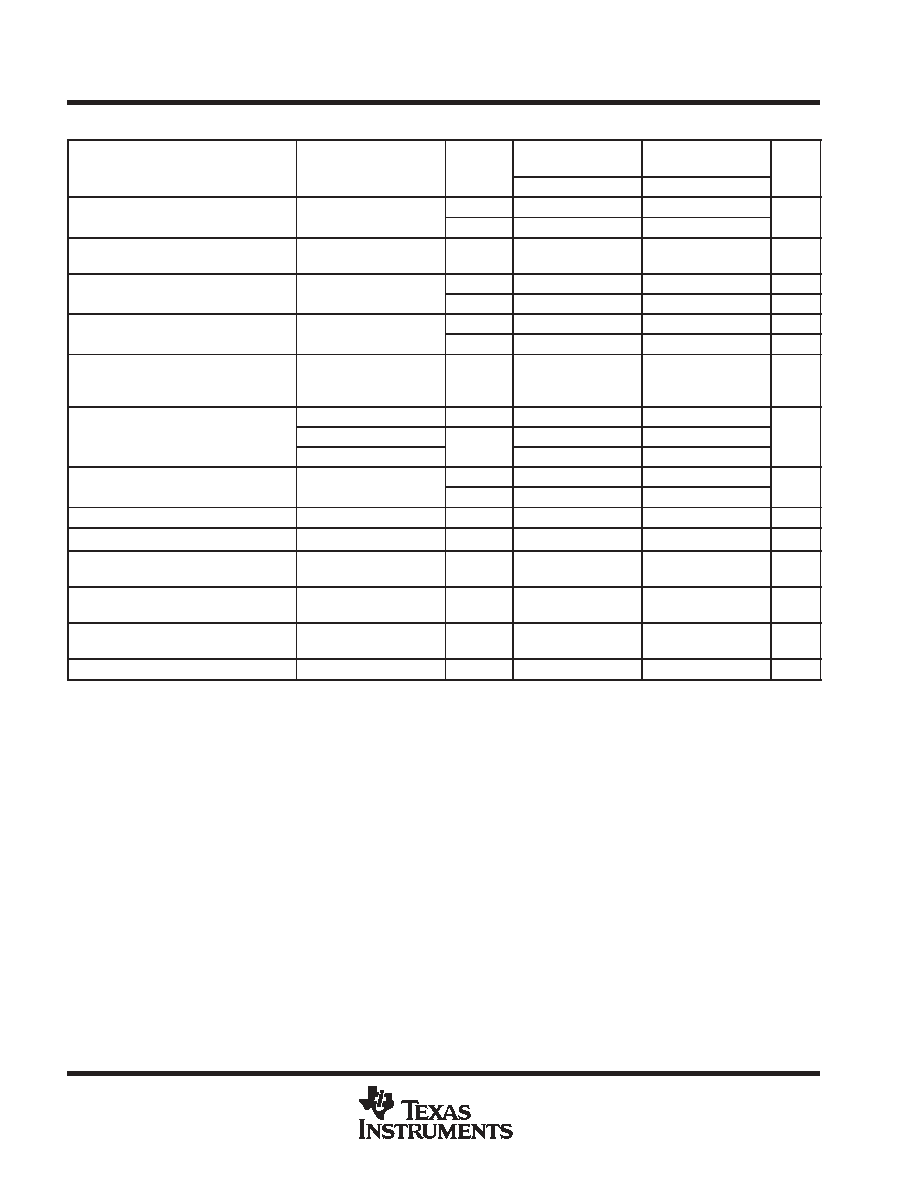
electrical characteristics, V
CC
±
=
±
15 V (unless otherwise noted)
TL071C
TL071AC
TL071BC
TL071I
P
ARAMETER
TEST CONDITIONS
T
A
TL071C
TL072C
TL071AC
TL072AC
TL071BC
TL072BC
TL071I
TL072I
UNIT
P
ARAMETER
TEST CONDITIONS
T
A
TL072C
TL074C
TL072AC
TL074AC
TL072BC
TL074BC
TL072I
TL074I
UNIT
A
MIN
TYP
MAX
MIN
TYP
MAX
MIN
TYP
MAX
MIN
TYP
MAX
V
IO
Input of
fset voltage
V
O
= 0,
R
S
= 50
25
°
C
3
10
3
6
2
3
3
6
mV
V
IO
Input of
fset voltage
V
O
= 0,
R
S
= 50
Full range
13
7.5
5
8
mV
V IO
T
emperature
coef
ficient of input
of
fset voltage
V
O
= 0,
R
S
= 50
Full range
18
18
18
18
µ
V/
°
C
I IO
Input of
fset current
V
O
= 0
25
°
C
5
100
5
100
5
100
5
100
pA
I IO
Input of
fset current
V
O
= 0
Full range
10
2
2
2
nA
I IB
Input bias current
§
V
O
= 0
25
°
C
65
200
65
200
65
200
65
200
pA
I IB
Input bias current
§
V
O
= 0
Full range
7
7
7
20
nA
Common-mode
-12
-12
-12
-12
V
ICR
Common-mode
input voltage range
25
°
C
±
11
-12
to
±
11
-12
to
±
11
-12
to
±
11
-12
to
V
V
ICR
input voltage range
25
C
±
11
to
15
±
11
to
15
±
11
to
15
±
11
to
15
V
Maximum peak
R
L
= 10 k
25
°
C
±
12
±
13.5
±
12
±
13.5
±
12
±
13.5
±
12
±
13.5
V
OM
Maximum peak
output voltage
swing
R
L
10 k
Full range
±
12
±
12
±
12
±
12
V
V
OM
output voltage
swing
R
L
2 k
Full range
±
10
±
10
±
10
±
10
A
VD
Large-signal
dif
ferential voltage
V
O
=
±
10 V
,
R
L
2 k
25
°
C
25
200
50
200
50
200
50
200
V/mV
A
VD
dif
ferential voltage
amplification
V
O
=
±
10 V
,
R
L
2 k
Full range
15
25
25
25
V/mV
B
1
Unity-gain
bandwidth
25
°
C
3
3
3
3
MHz
r i
Input resistance
25
°
C
10
12
10
12
10
12
10
12
CMRR
Common-mode
rejection ratio
V
IC
= V
ICR
min,
25
°
C
70
100
75
100
75
100
75
100
dB
CMRR
Common-mode
rejection ratio
V
O
= 0,
R
S
= 50
25
°
C
70
100
75
100
75
100
75
100
dB
k
SVR
Supply-voltage
rejection ratio
V
CC
=
±
9 V to
±
15 V
,
25
°
C
70
100
80
100
80
100
80
100
dB
k
SVR
rejection ratio
(
V
CC
±
/
V
IO
)
V
O
= 0,
R
S
= 50
25
°
C
70
100
80
100
80
100
80
100
dB
I CC
Supply current
V
O
= 0,
No load
25
°
C
1.4
2.5
1.4
2.5
1.4
2.5
1.4
2.5
mA
I CC
Supply current
(each amplifier)
V
O
= 0,
No load
25
°
C
1.4
2.5
1.4
2.5
1.4
2.5
1.4
2.5
mA
V
O1
/V
O2
Crosstalk
attenuation
A
VD
= 100
25
°
C
120
120
120
120
dB
All characteristics are measured under open-loop conditions with zero common-mode voltage, unless otherwise specified.
Full range is T
A
= 0
°
C to 70
°
C for TL07_C,TL07_AC, TL07_BC and is T
A
= -40
°
C to 85
°
C for TL07_I.
§
Input
bias currents of an FET
-input operational amplifier are
normal junction reverse currents, which are temperature sensitive
as shown in Figure 4. Pulse techniques must be used
that
maintain the junction temperature as close to the ambient temperature as possible.
TL071, TL071A, TL071B, TL072
TL072A, TL072B, TL074, TL074A, TL074B
LOW NOISE JFET INPUT OPERATIONAL AMPLIFIERS
SLOS080G - SEPTEMBER 1978 - REVISED SEPTEMBER 2003
8
POST OFFICE BOX 655303
·
DALLAS, TEXAS 75265
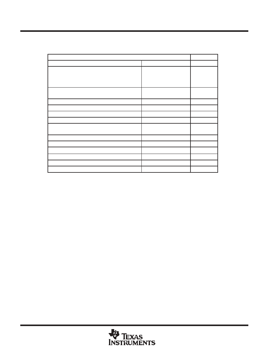
electrical characteristics, V
CC
±
=
±
15 V (unless otherwise noted)
TL071M
TL074M
PARAMETER
TEST CONDITIONS
TA
TL071M
TL072M
TL074M
UNIT
PARAMETER
TEST CONDITIONS
TA
MIN
TYP
MAX
MIN
TYP
MAX
UNIT
VIO
Input offset voltage
VO = 0,
RS = 50
25
°
C
3
6
3
9
mV
VIO
Input offset voltage
VO = 0,
RS = 50
Full range
9
15
mV
VIO
Temperature coefficient of
input offset voltage
VO = 0,
RS = 50
Full range
18
18
µ
V/
°
C
IIO
Input offset current
VO = 0
25
°
C
5
100
5
100
pA
IIO
Input offset current
VO = 0
Full range
20
20
nA
IIB
Input bias current
VO = 0
25
°
C
65
200
65
200
pA
IIB
Input bias current
VO = 0
50
50
nA
VICR
Common-mode input
voltage range
25
°
C
±
11
-12
to
15
±
11
-12
to
15
V
Maximum peak output
RL = 10 k
25
°
C
±
12
±
13.5
±
12
±
13.5
VOM
Maximum peak output
voltage swing
RL
10 k
Full range
±
12
±
12
V
VOM
voltage swing
RL
2 k
Full range
±
10
±
10
AVD
Large-signal differential
VO =
±
10 V,
RL
2 k
25
°
C
35
200
35
200
V/mV
AVD
Large-signal differential
voltage amplification
VO =
±
10 V,
RL
2 k
15
15
V/mV
B1
Unity-gain bandwidth
TA = 25
°
C
3
3
MHz
ri
Input resistance
TA = 25
°
C
1012
1012
CMRR
Common-mode rejection
VIC = VICRmin,
25
°
C
80
86
80
86
dB
CMRR
Common-mode rejection
ratio
VO = 0,
RS = 50
25
°
C
80
86
80
86
dB
kSVR
Supply-voltage rejection
VCC =
±
9 V to
±
15 V,
25
°
C
80
86
80
86
dB
kSVR
Supply-voltage rejection
ratio (
VCC
±
/
VIO)
VO = 0,
RS = 50
25
°
C
80
86
80
86
dB
ICC
Supply current (each
amplifier)
VO = 0,
No load
25
°
C
1.4
2.5
1.4
2.5
mA
VO1/VO2
Crosstalk attenuation
AVD = 100
25
°
C
120
120
dB
Input bias currents of an FET-input operational amplifier are normal junction reverse currents, which are temperature sensitive as shown in
Figure 4. Pulse techniques must be used that will maintain the junction temperature as close to the ambient temperature as possible.
All characteristics are measured under open-loop conditions with zero common-mode voltage, unless otherwise specified. Full range is
TA = -55
°
C to 125
°
C.

TL071, TL071A, TL071B, TL072
TL072A, TL072B, TL074, TL074A, TL074B
LOW NOISE JFET INPUT OPERATIONAL AMPLIFIERS
SLOS080G - SEPTEMBER 1978 - REVISED SEPTEMBER 2003
9
POST OFFICE BOX 655303
·
DALLAS, TEXAS 75265
operating characteristics, V
CC
±
=
±
15 V, T
A
= 25
°
C
PARAMETER
TEST CONDITIONS
TL07xM
ALL OTHERS
UNIT
PARAMETER
TEST CONDITIONS
MIN
TYP
MAX
MIN
TYP
MAX
UNIT
SR
Slew rate at unity gain
VI = 10 V,
CL = 100 pF,
RL = 2 k
,
See Figure 1
5
13
8
13
V/
µ
s
tr
Rise-time overshoot
VI = 20 mV,
RL = 2 k
,
0.1
0.1
µ
s
tr
Rise-time overshoot
factor
VI = 20 mV,
CL = 100 pF,
RL = 2 k
,
See Figure 1
20%
20%
Vn
Equivalent input noise
RS = 20
f = 1 kHz
18
18
nV/
Hz
Vn
Equivalent input noise
voltage
RS = 20
f = 10 Hz to 10 kHz
4
4
µ
V
In
Equivalent input noise
current
RS = 20
,
f = 1 kHz
0.01
0.01
pA/
Hz
THD
Total harmonic
distortion
VIrms = 6 V,
RL
2 k
,
f = 1 kHz
AVD = 1,
RS
1 k
,
0.003%
0.003%
PARAMETER MEASUREMENT INFORMATION
Figure 1. Unity-Gain Amplifier
VI
+
-
CL = 100 pF
RL = 2 k
VO
Figure 2. Gain-of-10 Inverting Amplifier
VI
+
-
10 k
1 k
RL
CL = 100 pF
VO
N1
100 k
+
-
TL071
N2
1.5 k
VCC-
OUT
IN-
IN+
Figure 3. Input Offset-Voltage Null Circuit
TL071, TL071A, TL071B, TL072
TL072A, TL072B, TL074, TL074A, TL074B
LOW NOISE JFET INPUT OPERATIONAL AMPLIFIERS
SLOS080G - SEPTEMBER 1978 - REVISED SEPTEMBER 2003
10
POST OFFICE BOX 655303
·
DALLAS, TEXAS 75265
TYPICAL CHARACTERISTICS
Table of Graphs
FIGURE
IIB
Input bias current
vs Free-air temperature
4
vs Frequency
5, 6, 7
VOM
Maximum output voltage
vs Frequency
vs Free-air temperature
5, 6, 7
8
VOM
Maximum output voltage
vs Free-air temperature
vs Load resistance
vs Supply voltage
8
9
10
vs Load resistance
vs Supply voltage
9
10
AVD
Large-signal differential voltage amplification
vs Free-air temperature
11
AVD
Large-signal differential voltage amplification
vs Free-air temperature
vs Frequency
11
12
Phase shift
vs Frequency
12
Normalized unity-gain bandwidth
vs Free-air temperature
13
Normalized phase shift
vs Free-air temperature
13
CMRR
Common-mode rejection ratio
vs Free-air temperature
14
ICC
Supply current
vs Supply voltage
15
ICC
Supply current
vs Supply voltage
vs Free-air temperature
15
16
PD
Total power dissipation
vs Free-air temperature
17
Normalized slew rate
vs Free-air temperature
18
Vn
Equivalent input noise voltage
vs Frequency
19
THD
Total harmonic distortion
vs Frequency
20
Large-signal pulse response
vs Time
21
VO
Output voltage
vs Elapsed time
22

TL071, TL071A, TL071B, TL072
TL072A, TL072B, TL074, TL074A, TL074B
LOW NOISE JFET INPUT OPERATIONAL AMPLIFIERS
SLOS080G - SEPTEMBER 1978 - REVISED SEPTEMBER 2003
11
POST OFFICE BOX 655303
·
DALLAS, TEXAS 75265
TYPICAL CHARACTERISTICS
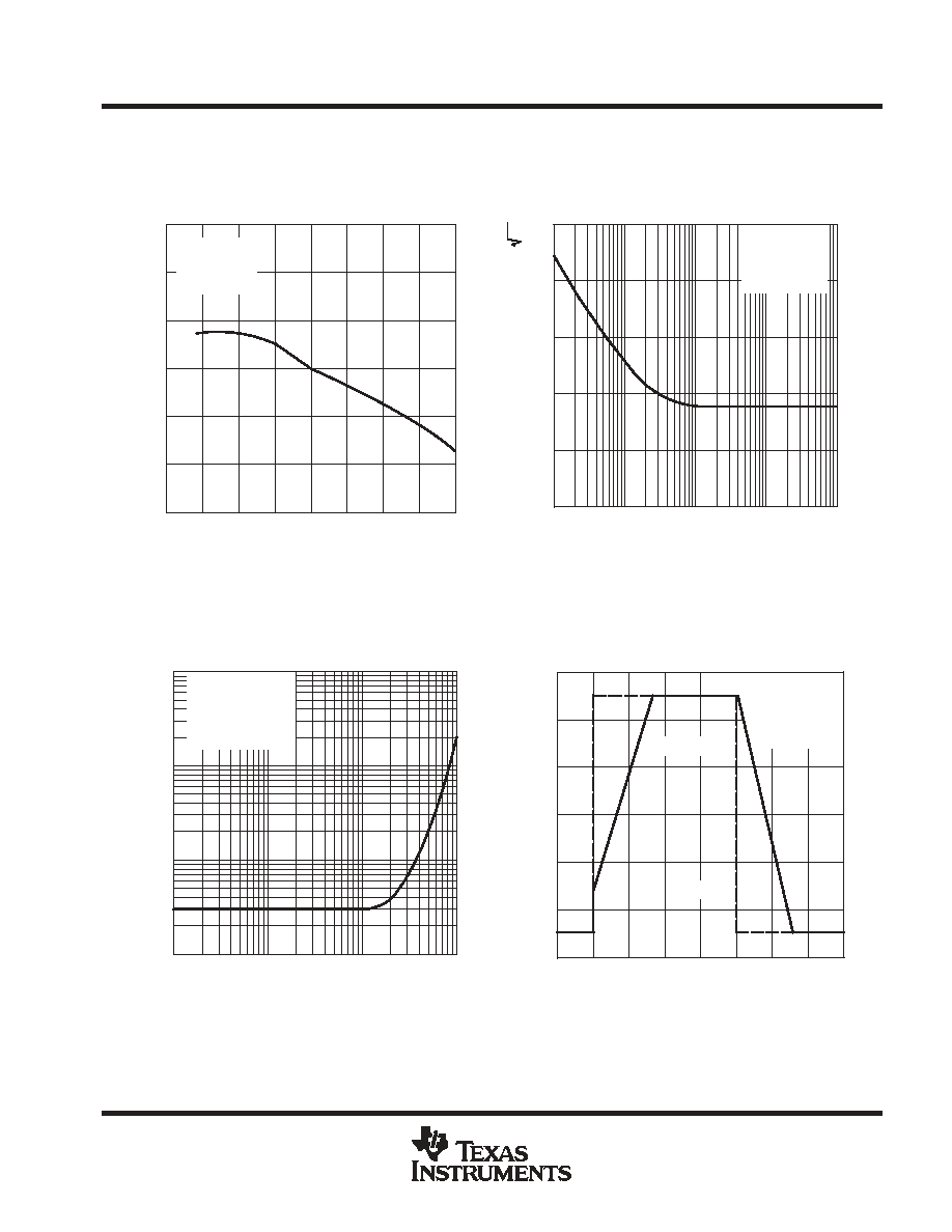
Figure 4
IIB- Input Bias Current - nA
TA - Free-Air Temperature -
°
C
INPUT BIAS CURRENT
vs
FREE-AIR TEMPERATURE
IBI
10
1
0.1
0.01
100
-75
-50
-25
0
25
50
75
100
125
VCC
±
=
±
15 V
Figure 5
RL = 10 k
TA = 25
°
C
See Figure 2
±
15
±
12.5
±
10
±
7.5
±
5
±
2.5
0
VOM - Maximum Peak Output V
o
ltage - V
f - Frequency - Hz
100
1 k
10 k
100 k
1 M
10 M
MAXIMUM PEAK OUTPUT VOLTAGE
vs
FREQUENCY
ÁÁÁ
ÁÁÁ
V
OM
ÎÎÎÎ
VCC
±
=
±
5 V
ÎÎÎÎÎ
VCC
±
=
±
10 V
ÎÎÎÎÎ
ÎÎÎÎÎ
VCC
±
=
±
15 V
Figure 6
10 M
1 M
100 k
10 k
1 k
100
f - Frequency - Hz
VOM - Maximum Peak Output V
oltage - V
0
±
2.5
±
5
±
7.5
±
10
±
12.5
±
15
See Figure 2
TA = 25
°
C
RL = 2 k
VCC
±
=
±
10 V
VCC
±
=
±
5 V
MAXIMUM PEAK OUTPUT VOLTAGE
vs
FREQUENCY
ÁÁ
ÁÁ
ÁÁ
V
OM
ÎÎÎÎÎ
ÎÎÎÎÎ
VCC
±
=
±
15 V
Figure 7
0
±
2.5
±
5
±
7.5
±
10
±
12.5
±
15
10 k
40 k
100 k
400 k
1 M
4 M
10 M
f - Frequency - Hz
MAXIMUM PEAK OUTPUT VOLTAGE
vs
FREQUENCY
VOM - Maximum Peak Output V
oltage - V
ÁÁÁ
ÁÁÁ
ÁÁÁ
V
OM
VCC
±
=
±
15 V
RL = 2 k
See Figure 2
ÎÎÎÎÎ
ÎÎÎÎÎ
TA = -55
°
C
ÎÎÎÎ
ÎÎÎÎ
TA = 25
°
C
TA = 125
°
C
Data at high and low temperatures are applicable only within the rated operating free-air temperature ranges of the various devices.

TL071, TL071A, TL071B, TL072
TL072A, TL072B, TL074, TL074A, TL074B
LOW NOISE JFET INPUT OPERATIONAL AMPLIFIERS
SLOS080G - SEPTEMBER 1978 - REVISED SEPTEMBER 2003
12
POST OFFICE BOX 655303
·
DALLAS, TEXAS 75265
TYPICAL CHARACTERISTICS
Figure 8
-75
0
VOM - Maximum Peak Output V
o
ltage - V
TA - Free-Air Temperature -
°
C
125
±
15
-50
-25
0
25
50
75
100
±
2.5
±
5
±
7.5
±
10
±
12.5
RL = 10 k
VCC
±
=
±
15 V
See Figure 2
MAXIMUM PEAK OUTPUT VOLTAGE
vs
FREE-AIR TEMPERATURE
ÁÁ
ÁÁ
V
OM
ÎÎÎÎ
ÎÎÎÎ
RL = 2 k
Figure 9
0.1
0
RL - Load Resistance - k
10
±
15
±
2.5
±
5
±
7.5
±
10
±
12.5
VCC
±
=
±
15 V
TA = 25
°
C
See Figure 2
0.2
0.4
0.7 1
2
4
7
MAXIMUM PEAK OUTPUT VOLTAGE
vs
LOAD RESISTANCE
VOM - Maximum Peak Output V
oltage - V
ÁÁ
ÁÁ
V
OM
Figure 10
0
0
VOM - Maximum Peak Output V
o
ltage - V
|VCC
±
| - Supply Voltage - V
16
±
15
2
4
6
8
10
12
14
±
2.5
±
5
±
7.5
±
10
±
12.5
RL = 10 k
TA = 25
°
C
MAXIMUM PEAK OUTPUT VOLTAGE
vs
SUPPLY VOLTAGE
ÁÁ
ÁÁ
ÁÁ
V
OM
Figure 11
-75
1
V
oltage
Amplification - V/mV
TA - Free-Air Temperature -
°
C
125
1000
-50
-25
0
25
50
75
100
2
4
10
20
40
100
200
400
VCC
±
=
±
15 V
VO =
±
10 V
RL = 2 k
LARGE-SIGNAL
DIFFERENTIAL VOLTAGE AMPLIFICATION
vs
FREE-AIR TEMPERATURE
A
VD - Large-Signal Differential
A
VD
Data at high and low temperatures are applicable only within the rated operating free-air temperature ranges of the various devices.

TL071, TL071A, TL071B, TL072
TL072A, TL072B, TL074, TL074A, TL074B
LOW NOISE JFET INPUT OPERATIONAL AMPLIFIERS
SLOS080G - SEPTEMBER 1978 - REVISED SEPTEMBER 2003
13
POST OFFICE BOX 655303
·
DALLAS, TEXAS 75265
TYPICAL CHARACTERISTICS
0
°
45
°
180
°
135
°
90
°
1
1
f - Frequency - Hz
10 M
106
10
100
1 k
10 k
100 k
1 M
101
102
103
104
105
Differential
Voltage
Amplification
VCC
±
=
±
5 V to
±
15 V
RL = 2 k
TA = 25
°
C
Phase Shift
LARGE-SIGNAL
DIFFERENTIAL VOLTAGE AMPLIFICATION
AND PHASE SHIFT
vs
FREQUENCY
V
oltage Amplification
A
VD - Large-Signal Differential
A
VD
Phase Shift
Figure 12
1.02
1.01
1
0.99
0.98
1.03
0.97
-75
0.7
Normalized Unity-Gain Bandwidth
TA - Free-Air Temperature -
°
C
125
1.3
-50
-25
0
25
50
75
100
0.8
0.9
1
1.1
1.2
Unity-Gain Bandwidth
VCC
±
=
±
15 V
RL = 2 k
f = B1 for Phase Shift
NORMALIZED UNITY-GAIN BANDWIDTH
AND PHASE SHIFT
vs
FREE-AIR TEMPERATURE
Normalized Phase Shift
Phase Shift
Figure 13
Data at high and low temperatures are applicable only within the rated operating free-air temperature ranges of the various devices.

TL071, TL071A, TL071B, TL072
TL072A, TL072B, TL074, TL074A, TL074B
LOW NOISE JFET INPUT OPERATIONAL AMPLIFIERS
SLOS080G - SEPTEMBER 1978 - REVISED SEPTEMBER 2003
14
POST OFFICE BOX 655303
·
DALLAS, TEXAS 75265
TYPICAL CHARACTERISTICS
Figure 14
-75
83
CMRR - Common-Mode Rejection Ratio - dB
TA - Free-Air Temperature -
°
C
125
89
-50
-25
0
25
50
75
100
84
85
86
87
88
VCC
±
=
±
15 V
RL = 10 k
COMMON-MODE REJECTION RATIO
vs
FREE-AIR TEMPERATURE
Figure 15
0
0
|VCC
±
| - Supply Voltage - V
16
2
2
4
6
8
10
12
14
0.2
0.4
0.6
0.8
1
1.2
1.4
1.6
1.8
TA = 25
°
C
No Signal
No Load
SUPPLY CURRENT PER AMPLIFIER
vs
SUPPLY VOLTAGE
ICC - Supply Current Per
Amplifier - mA
ÁÁ
ÁÁ
CC
±
I
Figure 16
-75
0
TA - Free-Air Temperature -
°
C
125
2
-50
-25
0
25
50
75
100
0.2
0.4
0.6
0.8
1
1.2
1.4
1.6
1.8
VCC
±
=
±
15 V
No Signal
No Load
SUPPLY CURRENT PER AMPLIFIER
vs
FREE-AIR TEMPERATURE
ICC - Supply Current Per
Amplifier - mA
ÁÁÁ
ÁÁÁ
ÁÁÁ
CC
±
I
Figure 17
-75
0
TA - Free-Air Temperature -
°
C
125
250
-50
-25
0
25
50
75
100
25
50
75
100
125
150
175
200
225
VCC
±
=
±
15 V
No Signal
No Load
TL074
TL071
TOTAL POWER DISSIPATION
vs
FREE-AIR TEMPERATURE
ÎÎÎÎ
ÎÎÎÎ
TL072
PD - T
otal Power Dissipation - mW
P
D
Data at high and low temperatures are applicable only within the rated operating free-air temperature ranges of the various devices.
TL071, TL071A, TL071B, TL072
TL072A, TL072B, TL074, TL074A, TL074B
LOW NOISE JFET INPUT OPERATIONAL AMPLIFIERS
SLOS080G - SEPTEMBER 1978 - REVISED SEPTEMBER 2003
15
POST OFFICE BOX 655303
·
DALLAS, TEXAS 75265
TYPICAL CHARACTERISTICS
Figure 18
-75
0.85
TA - Free-Air Temperature -
°
C
125
1.15
-50
-25
0
25
50
75
100
0.90
0.95
1
1.05
1.10
NORMALIZED SLEW RATE
vs
FREE-AIR TEMPERATURE
VCC
±
=
±
15 V
RL = 2 k
CL = 100 pF
s
µ
Normalized Slew Rate - V/
Figure 19
10
0
Vn - Equivalent Input Noise V
oltage - nV/Hz
f - Frequency - Hz
100 k
50
10
20
30
40
VCC
±
=
±
15 V
AVD = 10
RS = 20
TA = 25
°
C
40 100
400 1 k
4 k 10 k
40 k
EQUIVALENT INPUT NOISE VOLTAGE
vs
FREQUENCY
ÁÁÁ
ÁÁÁ
ÁÁÁ
ÁÁÁ
nV/
Hz
V
n
Figure 20
0.001
THD - T
otal Harmonic Distortion - %
1
40 k
10 k
4 k
1 k
400
100 k
f - Frequency - Hz
100
0.004
0.01
0.04
0.1
0.4
TOTAL HARMONIC DISTORTION
vs
FREQUENCY
VCC
±
=
±
15 V
AVD = 1
VI(RMS) = 6 V
TA = 25
°
C
Figure 21
-6
t - Time -
µ
s
3.5
6
0
0.5
1
1.5
2
2.5
3
-4
-2
0
2
4
Output
ÎÎÎ
ÎÎÎ
Input
VCC
±
=
±
15 V
RL = 2 k
TA = 25
°
C
VOLTAGE-FOLLOWER
LARGE-SIGNAL PULSE RESPONSE
CL = 100 pF
ÁÁ
ÁÁ
V
O
ÁÁ
ÁÁ
V
I
- Input and Output V
oltages - V
and

TL071, TL071A, TL071B, TL072
TL072A, TL072B, TL074, TL074A, TL074B
LOW NOISE JFET INPUT OPERATIONAL AMPLIFIERS
SLOS080G - SEPTEMBER 1978 - REVISED SEPTEMBER 2003
16
POST OFFICE BOX 655303
·
DALLAS, TEXAS 75265
TYPICAL CHARACTERISTICS
10%
-4
VO - Output V
oltage - mV
t - Elapsed Time -
µ
s
0.7
28
0
0.1
0.2
0.3
0.4
0.5
0.6
0
4
8
12
16
20
24
VCC
±
=
±
15 V
RL = 2 k
TA = 25
°
C
tr
Overshoot
90%
OUTPUT VOLTAGE
vs
ELAPSED TIME
ÁÁÁ
ÁÁÁ
V
O
Figure 22

TL071, TL071A, TL071B, TL072
TL072A, TL072B, TL074, TL074A, TL074B
LOW NOISE JFET INPUT OPERATIONAL AMPLIFIERS
SLOS080G - SEPTEMBER 1978 - REVISED SEPTEMBER 2003
17
POST OFFICE BOX 655303
·
DALLAS, TEXAS 75265
APPLICATION INFORMATION
Table of Application Diagrams
APPLICATION DIAGRAM
PART
NUMBER
FIGURE
0.5-Hz square-wave oscillator
TL071
23
High-Q notch filter
TL071
24
Audio-distribution amplifier
TL074
25
100-kHz quadrature oscillator
TL072
26
AC amplifier
TL071
27
Figure 23. 0.5-Hz Square-Wave Oscillator
+
-
-15 V
15 V
Output
1 k
9.1 k
3.3 k
CF = 3.3
µ
F
RF = 100 k
3.3 k
TL071
f
+
1
2
p
R
F
C
F
Figure 24. High-Q Notch Filter
+
-
R2
R1
C1
C2
R3
C3
VCC-
VCC+
TL071
Output
Input
C1
+
C2
+
C3
2
+
110 pF
f
O
+
1
2
p
R1 C1
+
1 kHz
R1
+
R2
+
2R3
+
1.5 M
W
100
µ
F
+
-
+
-
TL074
Output C
VCC+
VCC+
Output B
TL074
-
+
VCC+
Output A
TL074
-
+
VCC+
TL074
VCC+
100 k
Input
1
µ
F
1 M
100 k
100 k
VCC-
100 k
VCC-
VCC-
VCC-
Figure 25. Audio-Distribution Amplifier

TL071, TL071A, TL071B, TL072
TL072A, TL072B, TL074, TL074A, TL074B
LOW NOISE JFET INPUT OPERATIONAL AMPLIFIERS
SLOS080G - SEPTEMBER 1978 - REVISED SEPTEMBER 2003
18
POST OFFICE BOX 655303
·
DALLAS, TEXAS 75265
APPLICATION INFORMATION
-15 V
6 sin
t
+
-
6 cos
t
+
-
88.4 k
VCC+
VCC-
VCC+
VCC-
1N4148
18 pF
18 pF
1 k
18 k
(see Note A)
15 V
TL072
TL072
88.4 k
88.4 k
18 pF
1 k
18 k
(see Note A)
1N4148
NOTE A: These resistor values may be adjusted for a symmetrical output.
Figure 26. 100-kHz Quadrature Oscillator
0.1
µ
F
0.1
µ
F
+
-
10 k
50
100 k
N1
OUT
1 M
VCC+
10 k
10 k
TL071
N2
IN-
IN+
Figure 27. AC Amplifier
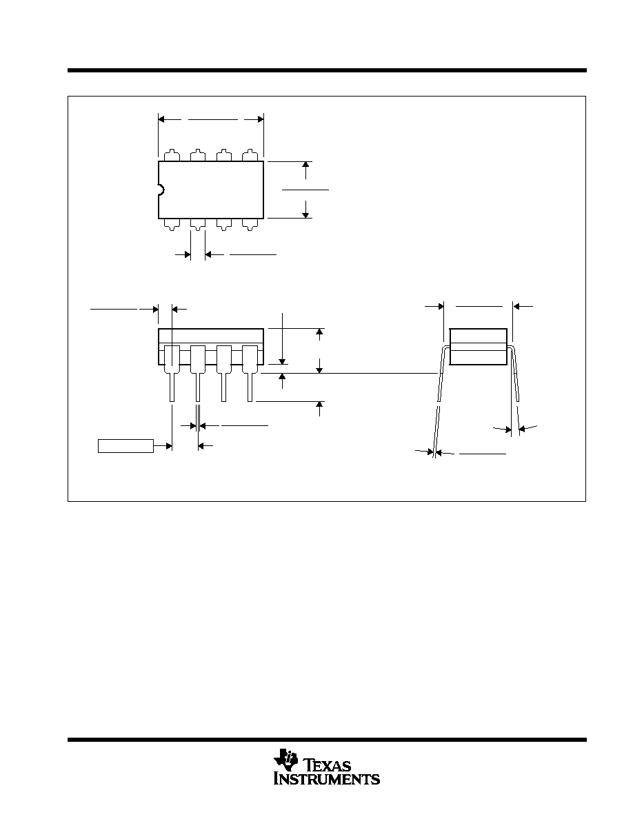
MECHANICAL DATA
MCER001A JANUARY 1995 REVISED JANUARY 1997
1
POST OFFICE BOX 655303
·
DALLAS, TEXAS 75265
JG (R-GDIP-T8)
CERAMIC DUAL-IN-LINE
0.310 (7,87)
0.290 (7,37)
0.014 (0,36)
0.008 (0,20)
Seating Plane
4040107/C 08/96
5
4
0.065 (1,65)
0.045 (1,14)
8
1
0.020 (0,51) MIN
0.400 (10,16)
0.355 (9,00)
0.015 (0,38)
0.023 (0,58)
0.063 (1,60)
0.015 (0,38)
0.200 (5,08) MAX
0.130 (3,30) MIN
0.245 (6,22)
0.280 (7,11)
0.100 (2,54)
0
°
15
°
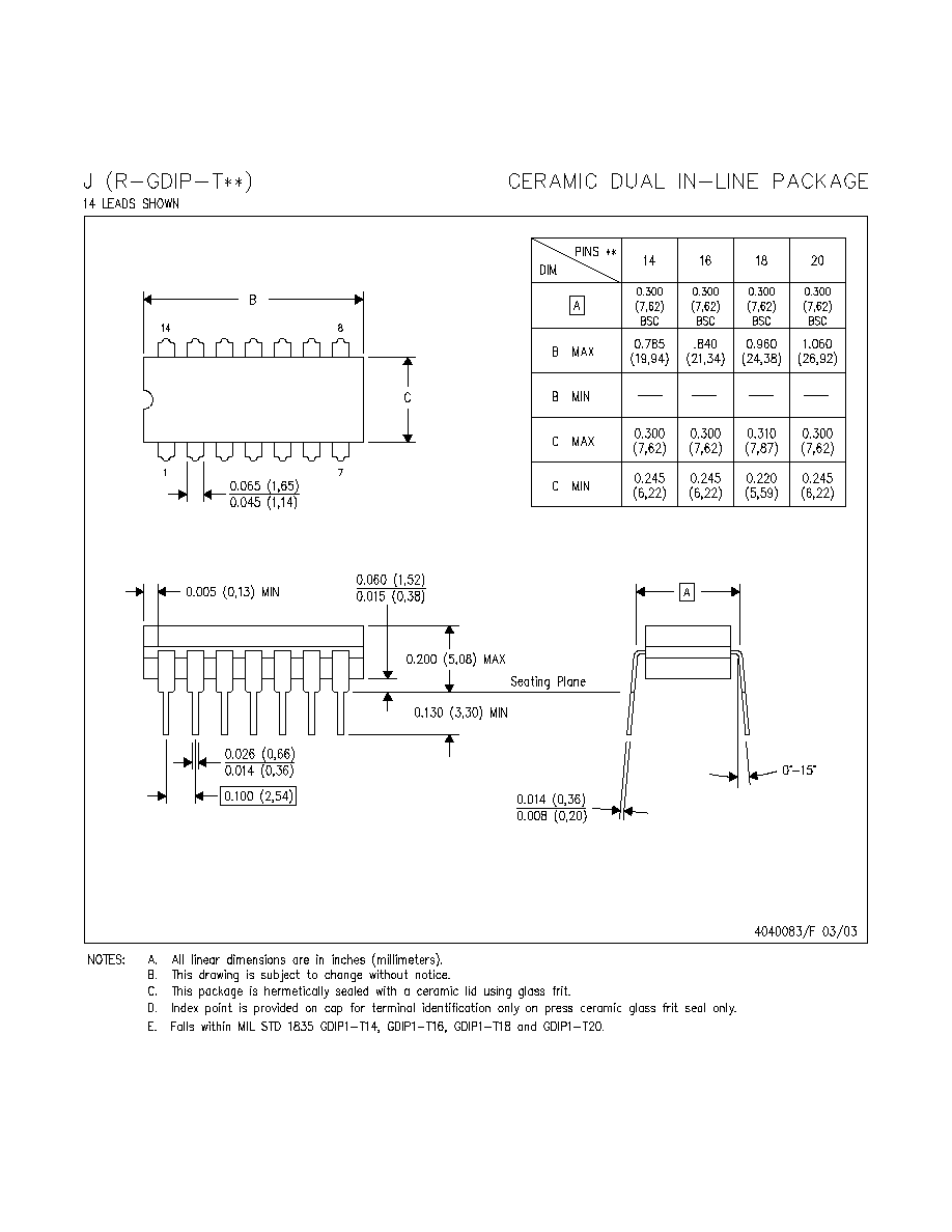
NOTES: A. All linear dimensions are in inches (millimeters).
B. This drawing is subject to change without notice.
C. This package can be hermetically sealed with a ceramic lid using glass frit.
D. Index point is provided on cap for terminal identification.
E. Falls within MIL STD 1835 GDIP1-T8

MECHANICAL DATA
MCFP001A JANUARY 1995 REVISED DECEMBER 1995
1
POST OFFICE BOX 655303
·
DALLAS, TEXAS 75265
U (S-GDFP-F10)
CERAMIC DUAL FLATPACK
4040179 / B 03/95
0.080 (2,03)
0.250 (6,35)
0.019 (0,48)
4 Places
0.300 (7,62) MAX
0.045 (1,14)
0.008 (0,20)
0.050 (1,27)
0.015 (0,38)
0.005 (0,13) MIN
0.026 (0,66)
0.004 (0,10)
0.246 (6,10)
1
10
5
6
0.250 (6,35)
0.350 (8,89)
0.350 (8,89)
0.250 (6,35)
0.050 (1,27)
Base and Seating Plane
0.280 (7,11)
0.230 (5,84)
NOTES: A. All linear dimensions are in inches (millimeters).
B. This drawing is subject to change without notice.
C. This package can be hermetically sealed with a ceramic lid using glass frit.
D. Index point is provided on cap for terminal identification only.
E. Falls within MIL STD 1835 GDFP1-F10 and JEDEC MO-092AA

MECHANICAL DATA
MCFP002A JANUARY 1995 REVISED FEBRUARY 2002
1
POST OFFICE BOX 655303
·
DALLAS, TEXAS 75265
W (R-GDFP-F14)
CERAMIC DUAL FLATPACK
0.360 (9,14)
0.250 (6,35)
8
7
14
1
0.235 (5,97)
0.004 (0,10)
0.026 (0,66)
4 Places
0.015 (0,38)
0.045 (1,14)
0.335 (8,51)
0.008 (0,20)
0.045 (1,14)
Base and Seating Plane
0.005 (0,13) MIN
0.019 (0,48)
0.390 (9,91)
0.260 (6,60)
0.080 (2,03)
4040180-2 / C 02/02
0.360 (9,14)
0.250 (6,35)
0.280 (7,11) MAX
0.050 (1,27)
NOTES: A. All linear dimensions are in inches (millimeters).
B. This drawing is subject to change without notice.
C. This package can be hermetically sealed with a ceramic lid using glass frit.
D. Index point is provided on cap for terminal identification only.
E. Falls within MIL STD 1835 GDFP1-F14 and JEDEC MO-092AB
MECHANICAL DATA
MLCC006B OCTOBER 1996
1
POST OFFICE BOX 655303
·
DALLAS, TEXAS 75265
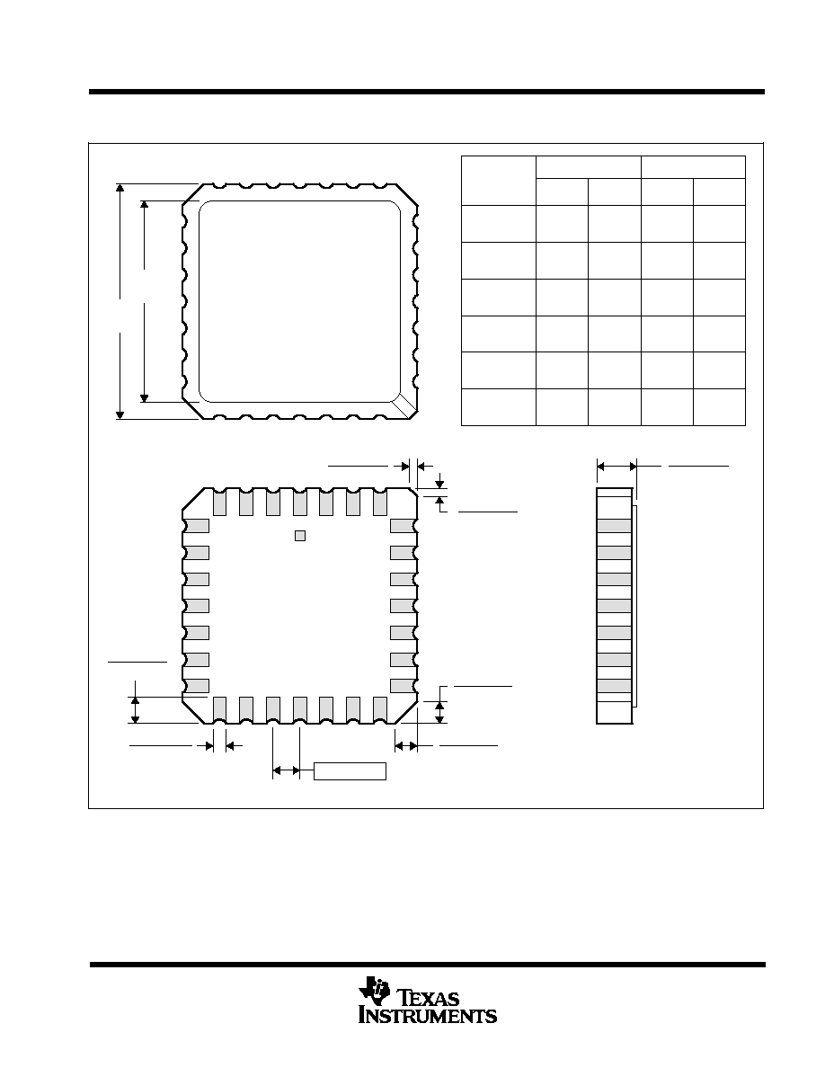
FK (S-CQCC-N**)
LEADLESS CERAMIC CHIP CARRIER
4040140 / D 10/96
28 TERMINAL SHOWN
B
0.358
(9,09)
MAX
(11,63)
0.560
(14,22)
0.560
0.458
0.858
(21,8)
1.063
(27,0)
(14,22)
A
NO. OF
MIN
MAX
0.358
0.660
0.761
0.458
0.342
(8,69)
MIN
(11,23)
(16,26)
0.640
0.739
0.442
(9,09)
(11,63)
(16,76)
0.962
1.165
(23,83)
0.938
(28,99)
1.141
(24,43)
(29,59)
(19,32)
(18,78)
**
20
28
52
44
68
84
0.020 (0,51)
TERMINALS
0.080 (2,03)
0.064 (1,63)
(7,80)
0.307
(10,31)
0.406
(12,58)
0.495
(12,58)
0.495
(21,6)
0.850
(26,6)
1.047
0.045 (1,14)
0.045 (1,14)
0.035 (0,89)
0.035 (0,89)
0.010 (0,25)
12
13
14
15
16
18
17
11
10
8
9
7
5
4
3
2
0.020 (0,51)
0.010 (0,25)
6
1
28
26
27
19
21
B SQ
A SQ
22
23
24
25
20
0.055 (1,40)
0.045 (1,14)
0.028 (0,71)
0.022 (0,54)
0.050 (1,27)
NOTES: A. All linear dimensions are in inches (millimeters).
B. This drawing is subject to change without notice.
C. This package can be hermetically sealed with a metal lid.
D. The terminals are gold plated.
E. Falls within JEDEC MS-004

MECHANICAL DATA
MPDI001A JANUARY 1995 REVISED JUNE 1999
1
POST OFFICE BOX 655303
·
DALLAS, TEXAS 75265
P (R-PDIP-T8)
PLASTIC DUAL-IN-LINE
8
4
0.015 (0,38)
Gage Plane
0.325 (8,26)
0.300 (7,62)
0.010 (0,25) NOM
MAX
0.430 (10,92)
4040082/D 05/98
0.200 (5,08) MAX
0.125 (3,18) MIN
5
0.355 (9,02)
0.020 (0,51) MIN
0.070 (1,78) MAX
0.240 (6,10)
0.260 (6,60)
0.400 (10,60)
1
0.015 (0,38)
0.021 (0,53)
Seating Plane
M
0.010 (0,25)
0.100 (2,54)
NOTES: A. All linear dimensions are in inches (millimeters).
B. This drawing is subject to change without notice.
C. Falls within JEDEC MS-001
For the latest package information, go to http://www.ti.com/sc/docs/package/pkg_info.htm
MECHANICAL
MPDI002C JANUARY 1995 REVISED DECEMBER 20002
1
POST OFFICE BOX 655303
·
DALLAS, TEXAS 75265
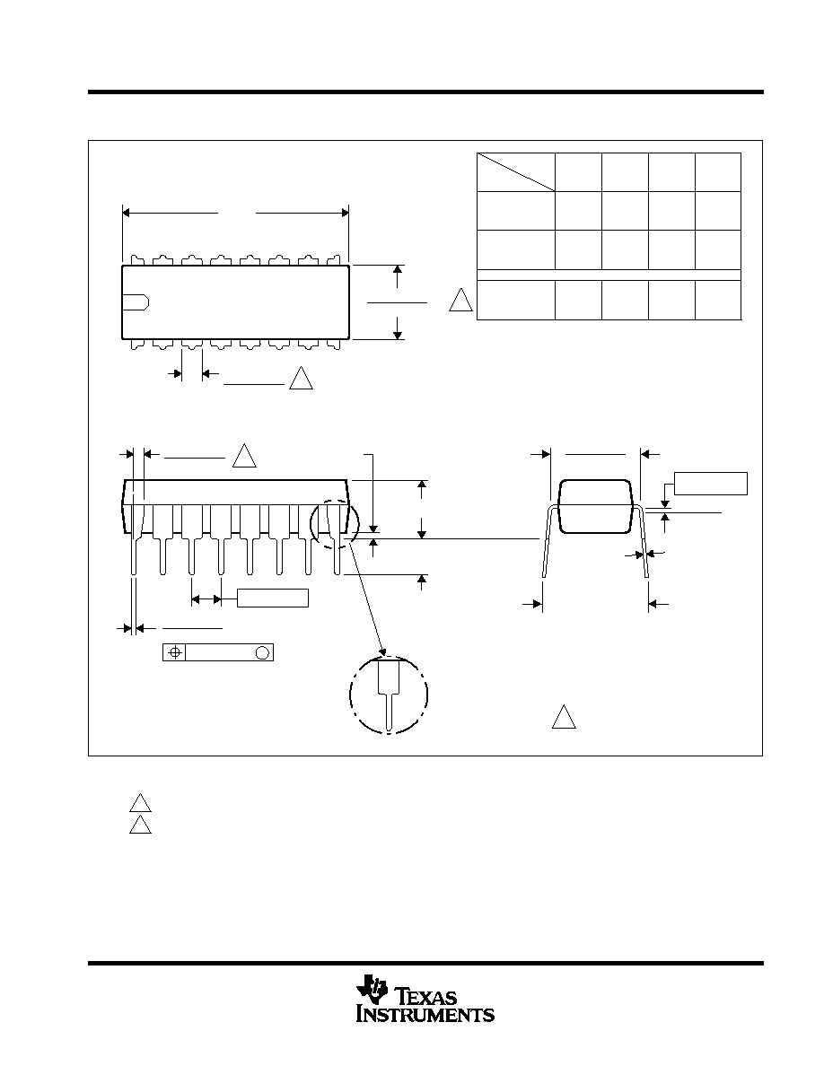
N (R-PDIP-T**)
PLASTIC DUAL-IN-LINE PACKAGE
BB
AC
AD
0.325 (8,26)
0.300 (7,62)
0.010 (0,25) NOM
Gauge Plane
0.015 (0,38)
0.430 (10,92) MAX
20
1.060
(26,92)
0.940
(23,88)
18
0.920
0.850
14
0.775
0.745
(19,69)
(18,92)
16
0.775
(19,69)
(18,92)
0.745
A MIN
DIM
A MAX
PINS **
(23,37)
(21,59)
Seating Plane
14/18 PIN ONLY
20 pin vendor option
4040049/E 12/2002
9
8
0.070 (1,78)
A
0.045 (1,14)
0.020 (0,51) MIN
16
1
0.015 (0,38)
0.021 (0,53)
0.200 (5,08) MAX
0.125 (3,18) MIN
0.240 (6,10)
0.260 (6,60)
M
0.010 (0,25)
0.100 (2,54)
16 PINS SHOWN
MS-100
VARIATION
AA
C
D
D
D
0.030 (0,76)
0.045 (1,14)
NOTES: A. All linear dimensions are in inches (millimeters).
B. This drawing is subject to change without notice.
C. Falls within JEDEC MS-001, except 18 and 20 pin minimum body lrngth (Dim A).
D. The 20 pin end lead shoulder width is a vendor option, either half or full width.
MECHANICAL DATA
MSOI002B JANUARY 1995 REVISED SEPTEMBER 2001
1
POST OFFICE BOX 655303
·
DALLAS, TEXAS 75265
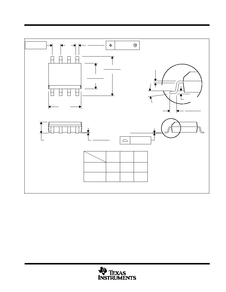
D (R-PDSO-G**)
PLASTIC SMALL-OUTLINE PACKAGE
8 PINS SHOWN
8
0.197
(5,00)
A MAX
A MIN
(4,80)
0.189
0.337
(8,55)
(8,75)
0.344
14
0.386
(9,80)
(10,00)
0.394
16
DIM
PINS **
4040047/E 09/01
0.069 (1,75) MAX
Seating Plane
0.004 (0,10)
0.010 (0,25)
0.010 (0,25)
0.016 (0,40)
0.044 (1,12)
0.244 (6,20)
0.228 (5,80)
0.020 (0,51)
0.014 (0,35)
1
4
8
5
0.150 (3,81)
0.157 (4,00)
0.008 (0,20) NOM
0
°
8
°
Gage Plane
A
0.004 (0,10)
0.010 (0,25)
0.050 (1,27)
NOTES: A. All linear dimensions are in inches (millimeters).
B. This drawing is subject to change without notice.
C. Body dimensions do not include mold flash or protrusion, not to exceed 0.006 (0,15).
D. Falls within JEDEC MS-012


MECHANICAL DATA
MTSS001C JANUARY 1995 REVISED FEBRUARY 1999
1
POST OFFICE BOX 655303
·
DALLAS, TEXAS 75265
PW (R-PDSO-G**)
PLASTIC SMALL-OUTLINE PACKAGE
14 PINS SHOWN
0,65
M
0,10
0,10
0,25
0,50
0,75
0,15 NOM
Gage Plane
28
9,80
9,60
24
7,90
7,70
20
16
6,60
6,40
4040064/F 01/97
0,30
6,60
6,20
8
0,19
4,30
4,50
7
0,15
14
A
1
1,20 MAX
14
5,10
4,90
8
3,10
2,90
A MAX
A MIN
DIM
PINS **
0,05
4,90
5,10
Seating Plane
0
°
8
°
NOTES: A. All linear dimensions are in millimeters.
B. This drawing is subject to change without notice.
C. Body dimensions do not include mold flash or protrusion not to exceed 0,15.
D. Falls within JEDEC MO-153

IMPORTANT NOTICE
Texas Instruments Incorporated and its subsidiaries (TI) reserve the right to make corrections, modifications,
enhancements, improvements, and other changes to its products and services at any time and to discontinue
any product or service without notice. Customers should obtain the latest relevant information before placing
orders and should verify that such information is current and complete. All products are sold subject to TI's terms
and conditions of sale supplied at the time of order acknowledgment.
TI warrants performance of its hardware products to the specifications applicable at the time of sale in
accordance with TI's standard warranty. Testing and other quality control techniques are used to the extent TI
deems necessary to support this warranty. Except where mandated by government requirements, testing of all
parameters of each product is not necessarily performed.
TI assumes no liability for applications assistance or customer product design. Customers are responsible for
their products and applications using TI components. To minimize the risks associated with customer products
and applications, customers should provide adequate design and operating safeguards.
TI does not warrant or represent that any license, either express or implied, is granted under any TI patent right,
copyright, mask work right, or other TI intellectual property right relating to any combination, machine, or process
in which TI products or services are used. Information published by TI regarding third-party products or services
does not constitute a license from TI to use such products or services or a warranty or endorsement thereof.
Use of such information may require a license from a third party under the patents or other intellectual property
of the third party, or a license from TI under the patents or other intellectual property of TI.
Reproduction of information in TI data books or data sheets is permissible only if reproduction is without
alteration and is accompanied by all associated warranties, conditions, limitations, and notices. Reproduction
of this information with alteration is an unfair and deceptive business practice. TI is not responsible or liable for
such altered documentation.
Resale of TI products or services with statements different from or beyond the parameters stated by TI for that
product or service voids all express and any implied warranties for the associated TI product or service and
is an unfair and deceptive business practice. TI is not responsible or liable for any such statements.
Following are URLs where you can obtain information on other Texas Instruments products and application
solutions:
Products
Applications
Amplifiers
amplifier.ti.com
Audio
www.ti.com/audio
Data Converters
dataconverter.ti.com
Automotive
www.ti.com/automotive
DSP
dsp.ti.com
Broadband
www.ti.com/broadband
Interface
interface.ti.com
Digital Control
www.ti.com/digitalcontrol
Logic
logic.ti.com
Military
www.ti.com/military
Power Mgmt
power.ti.com
Optical Networking
www.ti.com/opticalnetwork
Microcontrollers
microcontroller.ti.com
Security
www.ti.com/security
Telephony
www.ti.com/telephony
Video & Imaging
www.ti.com/video
Wireless
www.ti.com/wireless
Mailing Address:
Texas Instruments
Post Office Box 655303 Dallas, Texas 75265
Copyright
2003, Texas Instruments Incorporated