Document Outline
- FEATURES
- APPLICATIONS
- DESCRIPTION
- ORDERING INFORMATION
- PACKAGE DISSIPATION RATINGS
- ABSOLUTE MAXIMUM RATINGS
- RECOMMENDED OPERATING CONDITIONS
- ELECTRICAL CHARACTERISTICS
- PIN ASSIGNMENTS
- TYPICAL CHARACTERISTICS

THS6182
SLLS544E SEPTEMBER 2002 REVISED JULY 2003
LOW POWER DISSIPATION ADSL LINE DRIVER
FEATURES
D
Low Power Dissipation Increases ADSL Line
Card Density
D
Low THD of 88 dBc (100-
, 1 MHz)
D
Low MTPR Driving +20 dBm on the Line
76 dBc With High Bias Setting
74 dBc With Low Bias Setting
D
Wide Output Swing of 44V
PP
Differential Into
a 200
Differential Load (V
CC
=
±
12 V)
D
High Output Current of 600 mA (Typ)
D
Wide Supply Voltage Range of
±
5 V to
±
15 V
D
Pin Compatible With EL1503C and EL1508C
Multiple Package Options
D
Multiple Power Control Modes
11 mA/ch Full Bias Mode
7.5 mA/ch Mid Bias Mode
4 mA/ch Low Bias Mode
0.25 mA/ch Shutdown Mode
I
ADJ
Pin for User Controlled Bias Current
Stable Operation Down to 2 mA/ch
D
Low Noise for Increased Receiver Sensitivity
3.2 nV/
Hz Voltage Noise
1.5 pA/
Hz Noninverting Current Noise
10 pA/
Hz Inverting Current Noise
APPLICATIONS
D
Ideal for Full Rate ADSL Applications
DESCRIPTION
The THS6182 is a current feedback differential line driver
ideal for full rate ADSL systems. Its extremely low power
dissipation is ideal for ADSL systems that must achieve
high densities in ADSL central office rack applications.
The unique architecture of the THS6182 allows the
quiescent current to be much lower than existing line
drivers while still achieving very high linearity without the
need for excess open loop gain. Fixed multiple bias
settings of the amplifiers allow for enhanced power
savings for line lengths where the full performance of the
amplifier is not required. To allow for even more flexibility
and power savings, an I
ADJ
pin is available to further lower
the bias currents while maintaining stable operation with
as little as 2 mA per channel. The wide output swing of 44
V
pp
differentially with
±
12V power supplies allows for more
dynamic headroom, keeping distortion at a minimum. With
a low 3.2 nV/
Hz voltage noise coupled with a low
10 pA/
Hz inverting current noise, the THS6182
increases the sensitivity of the receive signals, allowing for
better margins and reach.
Typical ADSL CO Line Driver Circuit Utilizing Active Impedance
+
THS6182a
+12V
12V
+
1:1.2
12V
+12V
8.68
100
1 k
1 k
1.33 k
1.33 k
953
CODEC
V
IN
CODEC
V
IN+
8.68
+20 dBm
Line
Power
THS6182b
PRODUCTION DATA information is current as of publication date. Products
conform to specifications per the terms of Texas Instruments standard warranty.
Production processing does not necessarily include testing of all parameters.
Please be aware that an important notice concerning availability, standard warranty, and use in critical applications of Texas Instruments
semiconductor products and disclaimers thereto appears at the end of this data sheet.
www.ti.com
Copyright
2002 2003, Texas Instruments Incorporated

THS6182
SLLS544E SEPTEMBER 2002 REVISED JULY 2003
www.ti.com
2
These devices have limited built-in ESD protection. The leads should be shorted together or the device placed in conductive foam during
storage or handling to prevent electrostatic damage.
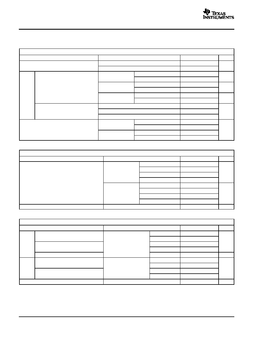
ORDERING INFORMATION
PRODUCT
PACKAGE
PACKAGE
SYMBOL
T
ORDER
TRANSPORT MEDIA
PRODUCT
PACKAGE
PACKAGE
CODE
SYMBOL
TA
ORDER
NUMBER
TRANSPORT MEDIA
THS6182RHF
Leadless 24-pin 4 mm x
RHF24
6182
THS6182RHFR
Tape and reel
(3000 devices)
THS6182RHF
Leadless 24 in 4 mm x
5 mm PowerPAD
RHF24
6182
THS6182RHFT
Tape and reel
(250 devices)
40
°
C to 85
°
C
THS6182D
Tube (40 devices)
THS6182D
SOIC16
D16
THS6182
40
°
C to 85
°
C
THS6182DR
Tape and reel
(2500 devices)
THS6182DW
Tube (25 devices)
THS6182DW
SOIC20
DW20
THS6182
THS6182DWR
Tape and reel
(2000 devices)
PACKAGE DISSIPATION RATINGS
(1)
PACKAGE
PowerPAD
SOLDERED(2)
JA
PowerPAD
NOT SOLDERED(3)
JA
JC
RHF-24
32
°
C/W
74
°
C/W
1.7
°
C/W
D-16
62.9
°
C/W
25.7
°
C/W
DW-20
45.4
°
C/W
16.4
°
C/W
(1)
JA values shown are typical for standard test PCBs only.
(2) For high power dissipation
applications, use of the PowerPAD package and soldering the PowerPAD to the PCB is required. Failure to do so
may result in reduced reliability and/or lifetime of the device. See TI technical brief SLMA002 for more information about utilizing the PowerPAD
thermally enhanced package.
(3) Use of packages without the PowerPAD or not soldering the PowerPAD to the PCB, should be limited to low-power dissipation applications.
ABSOLUTE MAXIMUM RATINGS
over operating free-air temperature range unless otherwise noted(1)
ELECTRICAL
THS6182
Supply voltage, VCC(2)
±
16.5 V
Input voltage, VI
±
VCC
Output current, IO (2)
1000 mA
Differential input voltage, VIO
±
2 V
THERMAL
Maximum junction temperature, any condition(3), TJ
150
°
C
Maximum junction temperature, continuous operation, long term reliability(4), TJ
125
°
C
Operating freeair temperature, TA
40
°
C to 85
°
C
Storage temperature, Tsgt
65
°
C to 150
°
C
Lead temperature, 1,6 mm (1/16inch) from case for 10 seconds
300
°
C
(1) Stresses beyond those listed under "absolute maximum ratings" may cause permanent damage to the device. These are stress ratings only, and
functional operation of the device at these or any other conditions beyond those indicated under "recommended operating conditions" is not
implied. Exposure to absolute-maximum-rated conditions for extended periods may affect device reliability.
(2) The THS6182 may incorporate a PowerPAD on the underside of the chip. This acts as a heatsink and must be connected to a thermally
dissipating plane for proper power dissipation. Failure to do so may result in exceeding the maximum junction temperature that could
permanently damage the device. See TI Technical Brief SLMA002 for more information about utilizing the PowerPAD thermally enhanced
package.
(3) The absolute maximum temperature under any condition is limited by the constraints of the silicon process.
(4) The maximum junction temperature for continuous operation is limited by package constraints. Operation above this temperature may result
in reduced reliability and/or lifetime of the device.

THS6182
SLLS544E SEPTEMBER 2002 REVISED JULY 2003
www.ti.com
3
ABSOLUTE MAXIMUM RATINGS
ESD
HBM
500 V
ESD ratings
CDM
1500 V
ESD ratings
MM
200 V
RECOMMENDED OPERATING CONDITIONS
MIN
NOM
MAX
UNIT
Supply voltage V
to V
Dual supply
±
5
±
12
±
15
V
Supply voltage, VCC+ to VCC
Single supply
10
24
30
V
Operating free-air temperature, TA
40
85
°
C
Operating junction temperature, continuous operation TJ
40
125
°
C
Normal storage temperature, Tstg
40
85
°
C
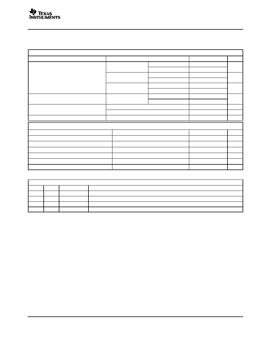
ELECTRICAL CHARACTERISTICS
over recommended operating free-air temperature range, TA = 25
°
C,VCC =
±
12 V, RF = 2 k
, Gain = +5, IADJ = Bias1 = Bias2 = 0 V, RL = 50
(unless otherwise noted)
NOISE/DISTORTION PERFORMANCE
PARAMETER
TEST CONDITIONS
MIN
TYP
MAX
UNIT
MTPR
Multitone power ratio
Gain =+9.5, 163 kHz to 1.1 MHz DMT,
+20 dBm Line Power, See Figure 1 for circuit
76
dBc
Receive band spillover
Gain =+5, 25 kHz to 138 kHz with MTPR signal applied,
See Figure 1 for circuit
95
dBc
2nd harmonic
Differential load = 200
88
dBc
HD
Harmonic distortion, VO(PP) = 2 V
2nd harmonic
Differential load = 50
70
dBc
HD
Harmonic distortion, VO(PP) = 2 V
f = 1 MHz
3rd harmonic
Differential load = 200
107
dBc
3rd harmonic
Differential load = 50
84
dBc
Vn
Input voltage noise
VCC =
±
5 V,
±
12 V,
±
15 V, f = 100 kHz
3.2
nV/
Hz
I
Input current
+Input
VCC =
±
5 V
±
12 V
±
15 V
f = 100 kHz
1.5
pA/
Hz
In
In ut current
noise
Input
VCC =
±
5 V,
±
12 V,
±
15 V, f = 100 kHz
10
pA/
Hz
Crosstalk
f = 1 MHz, VO(PP) = 2 V,
RL = 100
65
dBc
Crosstalk
f = 1 MHz, VO(PP) = 2 V,
VCC =
±
5 V,
±
12 V,
±
15 V
RL = 25
60
dBc
OUTPUT CHARACTERISTICS
VCC =
±
5 V
RL = 100
±
3.9
±
4.1
V
VCC =
±
5 V
RL = 25
±
3.7
±
3.9
V
VO
Single ended output voltage swing
VCC =
±
12 V
RL = 100
±
10.7
±
11.0
V
VO
Single-ended output voltage swing
VCC =
±
12 V
RL = 25
±
10.0
±
10.6
V
VCC =
±
15 V
RL = 100
±
13.5
±
13.9
V
VCC =
±
15 V
RL = 25
±
12.7
±
13.4
V
RL = 5
VCC =
±
5 V
±
350
±
400
I
O
Output current (1)
RL = 10
VCC =
±
12 V
±
450
±
600
mA
I
O
Out ut current ( )
RL = 10
VCC =
±
15 V
±
450
±
600
mA
I(SC)
Short-circuit current (1)
RL = 1
VCC =
±
12 V
1000
mA
Output resistance
Open-loop
6
Output resistance--terminate mode
f = 1 MHz,
Gain = +10
0.05
Output resistance--shutdown mode
f = 1 MHz,
Open-loop
8.5
k
(1) A heatsink is rsequired to keep the junction temperature below absoulte maximum rating when an output is heavily loaded or shorted. See
Absolute Maximum Ratings section for more information.
THS6182
SLLS544E SEPTEMBER 2002 REVISED JULY 2003
www.ti.com
4
ELECTRICAL CHARACTERISTICS (continued)
over recommended operating free-air temperature range, TA = 25
°
C,VCC =
±
12 V, RF = 2 k
, Gain = +5, IADJ = Bias1 = Bias2 = 0 V, RL = 50
(unless otherwise noted)
POWER SUPPLY
PARAMETER
TEST CONDITIONS
MIN
TYP
MAX
UNIT
VCC
Operating range
Dual supply
±
4
±
12
±
16.5
V
VCC
Operating range
Single supply
8
24
33
V
VCC =
±
5 V
TA = 25
°
C
9.7
10.7
mA
Quiescent current (each driver)(1)
VCC =
±
5 V
TA = full range
11.7
mA
Quiescent current (each driver)(1)
Full-bias mode
VCC =
±
12 V
TA = 25
°
C
11
12
mA
Full-bias mode
(Bias1 = 0, Bias2 = 0)
(T i
d ith V
±
15 V t 25
°
C)
VCC =
±
12 V
TA = full range
12.5
mA
I
CC
(
,
)
(Trimmed with VCC =
±
15 V at 25
°
C)
VCC =
±
15 V
TA = 25
°
C
11.5
12.5
mA
I
CC
VCC =
±
15 V
TA = full range
13
mA
Q i
t
t (
h d i
)
Mid; Bias1 = 1, Bias2 = 0
7.5
8.5
Quiescent current (each driver)
Variable bias modes VCC =
±
12 V
Low; Bias1 = 0, Bias2 = 1
4
5
mA
Variable bias modes, VCC =
±
12 V
Shutdown; Bias1 = 1, Bias2 = 1
0.25
0.9
mA
VCC =
±
5 V,
TA = 25
°
C
50
56
PSRR
Power supply rejection ratio
VCC
±
5 V,
VCC =
±
0.5 V
TA = full range
47
dB
PSRR
Power su
ly rejection ratio
(
VCC =
±
1 V)
VCC =
±
12 V,
±
15 V,
TA = 25
°
C
56
60
dB
(
CC
)
VCC
±
12 V,
±
15 V,
VCC =
±
1 V
TA = full range
53
(1) Approximately 0.5 mA (total) flows from VCC+ to GND for internal logic control bias.
DYNAMIC PERFORMANCE
PARAMETER
TEST CONDITIONS
MIN
TYP
MAX
UNIT
Gain = +1, RF = 1.2 k
100
RL = 100
Gain = +2, RF = 1 k
80
MHz
RL = 100
Gain = +5, RF = 1 k
35
MHz
BW
Single-ended small-signal bandwidth
Gain = +10, RF = 1 k
20
BW
Single ended small signal bandwidth
(3 dB), VO = 0.1 Vrms
Gain = +1, RF = 1.5k
65
( 3 dB), VO 0.1 Vrms
RL = 25
Gain = +2, RF = 1 k
60
MHz
RL = 25
Gain = +5, RF = 1 k
40
MHz
Gain = +10, RF = 1 k
22
SR
Single-ended slew-rate(2)
VO = 10 VPP,
Gain =+5
450
V/
µ
s
(2) Slew-rate is defined from the 25% to the 75% output levels
DC PERFORMANCE
PARAMETER
TEST CONDITIONS
MIN
TYP
MAX
UNIT
Input offset voltage
TA = 25
°
C
1
20
Input offset voltage
TA = full range
25
mV
V
OS
Differential offset voltage
VCC =
±
5 V,
±
12 V,
±
15 V
TA = 25
°
C
0.5
10
mV
V
OS
Differential offset voltage
VCC
±
5 V,
±
12 V,
±
15 V
TA = full range
15
Offset drift
TA = full range
50
µ
V/
°
C
Input bias current
TA = 25
°
C
8
15
I
Input bias current
VCC =
±
5 V
±
12 V
±
15 V
TA = full range
20
µ
A
I
IB
+ Input bias current
VCC =
±
5 V,
±
12 V,
±
15 V
TA = 25
°
C
8
15
µ
A
+ Input bias current
TA = full range
20
Z
OL
Open loop transimpedance
RL = 1 k
,
VCC =
±
12 V,
±
15 V,
900
k
THS6182
SLLS544E SEPTEMBER 2002 REVISED JULY 2003
www.ti.com
5
ELECTRICAL CHARACTERISTICS (CONTINUED)
over recommended operating free-air temperature range, TA = 25
°
C,VCC =
±
12 V, RF = 2 k
, Gain = +5, IADJ = Bias1 = Bias2 = 0 V, RL = 50
(unless otherwise noted)
INPUT CHARACTERISTICS
PARAMETER
TEST CONDITIONS
MIN
TYP
MAX
UNIT
VCC
±
5 V
TA = 25
°
C
±
2.7
±
3.0
V
VCC =
±
5 V
TA = full range
±
2.6
V
V
Input common mode voltage range
VCC
±
12 V
TA = 25
°
C
±
9.5
±
9.8
V
V
ICR
Input commonmode voltage range
VCC =
±
12 V
TA = full range
±
9.3
V
VCC
±
15 V
TA = 25
°
C
±
12.4
±
12.7
V
VCC =
±
15 V
TA = full range
±
12.1
V
CMRR
Common mode rejection ratio
VCC
±
5 V
±
12 V
±
15 V
TA = 25
°
C
48
54
dB
CMRR
Common-mode rejection ratio
VCC =
±
5 V,
±
12 V,
±
15 V
TA = full range
44
dB
R
Input resistance
+ Input
800
k
R
I
Input resistance
Input
30
C
I
Input capacitance
1.7
pF
LOCIC CONTROL CHARACTERISTICS
PARAMETER
TEST CONDITIONS
MIN
TYP
MAX
UNIT
VIH
Bias pin voltage for logic 1
Relative to GND pin voltage
2.0
V
VIL
Bias pin voltage for logic 0
Relative to GND pin voltage
0.8
V
IIH
Bias pin current for logic 1
VIH = 3.3 V, GND = 0 V
4
30
µ
A
IIL
Bias pin current for logic 0
VIL = 0.5 V, GND = 0 V
1
10
µ
A
Transition time--logic 0 to logic 1(1)
1
µ
s
Transition time--logic 1 to logic 0(1)
1
µ
s
(1) Transition time is defined as the time from when the logic signal is applied to the time when the supply current has reached half its final value.
LOGIC TABLE
BIAS-1
BIAS-2
FUNCTION
DESCRIPTION
0
0
Full bias mode
Amplifiers ON with lowest distortion possible (default state)
1
0
Mid bias mode
Amplifiers ON with power savings with a reduction in distortion performance
0
1
Low bias mode
Amplifiers ON with enhanced power savings and a reduction of distortion performance
1
1
Shutdown mode
Amplifiers OFF and output has high impedance
NOTE: The default state for all logic pins is a logic zero (0).